Xray CCD Detectors for Astronomy and Space Science
- Slides: 34

X-ray CCD Detectors for Astronomy and Space Science Andrew Holland a. d. holland@open. ac. uk

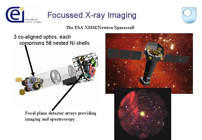
Focussed X-ray Imaging The ESA XMM/Newton Spacecraft 3 co-aligned optics, each comprising 58 nested Ni shells Focal plane detector arrays providing imaging and spectroscopy

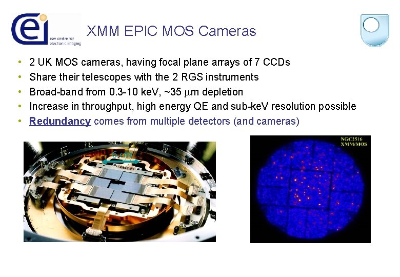
XMM EPIC MOS Cameras • • • 2 UK MOS cameras, having focal plane arrays of 7 CCDs Share their telescopes with the 2 RGS instruments Broad-band from 0. 3 -10 ke. V, ~35 mm depletion Increase in throughput, high energy QE and sub-ke. V resolution possible Redundancy comes from multiple detectors (and cameras) 6 cm

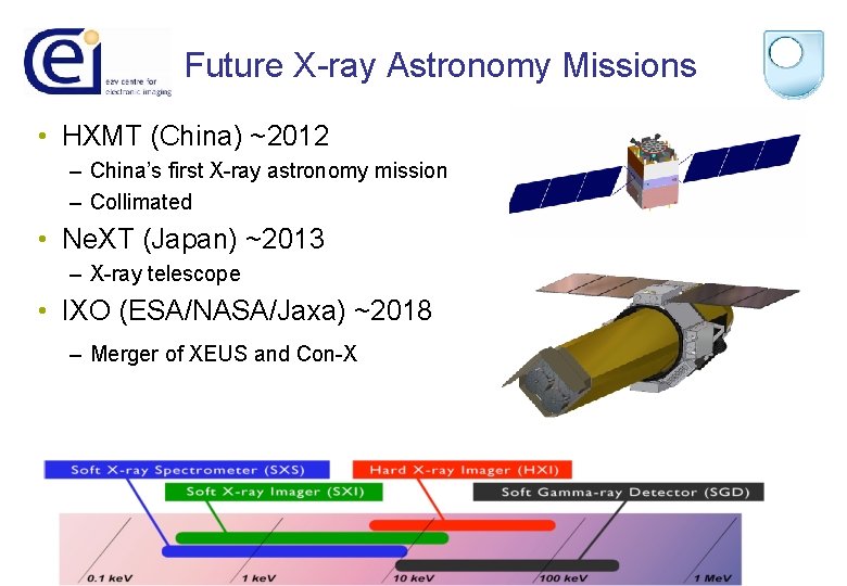
Future X-ray Astronomy Missions • HXMT (China) ~2012 – China’s first X-ray astronomy mission – Collimated • Ne. XT (Japan) ~2013 – X-ray telescope • IXO (ESA/NASA/Jaxa) ~2018 – Merger of XEUS and Con-X

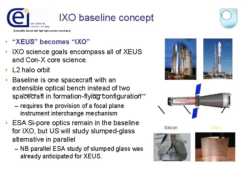
IXO baseline concept Extendible Bench with light tight curtain (not shown) • “XEUS” becomes “IXO” • IXO science goals encompass all of XEUS and Con-X core science. • L 2 halo orbit • Baseline is one spacecraft with an extensible optical bench instead of two spacecraft in formation-flying configuration Focal Plane Spacecraft bus Mirror – requires the provision of a focal plane instrument interchange mechanism • ESA Si-pore optics remain in the baseline for IXO, but US will study slumped-glass alternative in parallel – NB parallel ESA study of slumped glass was already anticipated for XEUS. Silicon Glass

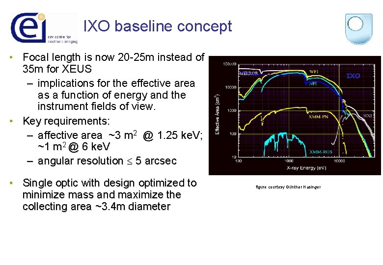
IXO baseline concept • Focal length is now 20 -25 m instead of 35 m for XEUS – implications for the effective area as a function of energy and the instrument fields of view. • Key requirements: – affective area ~3 m 2 @ 1. 25 ke. V; ~1 m 2 @ 6 ke. V – angular resolution 5 arcsec • Single optic with design optimized to minimize mass and maximize the collecting area ~3. 4 m diameter figure courtesy Günther Hasinger

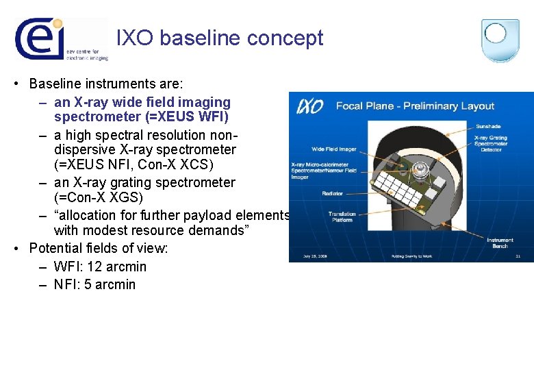
IXO baseline concept • Baseline instruments are: – an X-ray wide field imaging spectrometer (=XEUS WFI) – a high spectral resolution nondispersive X-ray spectrometer (=XEUS NFI, Con-X XCS) – an X-ray grating spectrometer (=Con-X XGS) – “allocation for further payload elements with modest resource demands” • Potential fields of view: – WFI: 12 arcmin – NFI: 5 arcmin figure courtesy Nick White

Key Reasons to Continue MOS Activity • Complementary technology to DEPFET – Reduces Technical Risk – Instrument Background • Instrument background IS lower in the XMM MOS CCDs – Redundancy • Key unknown risk of micrometeorite hit killing FPA • 2 separate WFI sub-systems virtually remove risk of catastrophic failure • Hope to re-introduce increased FOV for WFI

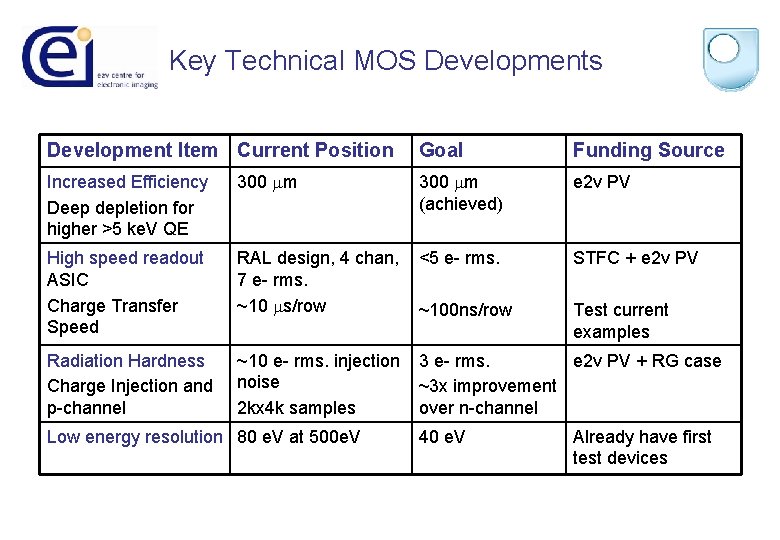
Key Technical MOS Developments Development Item Current Position Goal Funding Source Increased Efficiency Deep depletion for higher >5 ke. V QE 300 mm (achieved) e 2 v PV High speed readout ASIC Charge Transfer Speed RAL design, 4 chan, 7 e- rms. ~10 ms/row <5 e- rms. STFC + e 2 v PV ~100 ns/row Test current examples Radiation Hardness Charge Injection and p-channel ~10 e- rms. injection noise 2 kx 4 k samples 3 e- rms. e 2 v PV + RG case ~3 x improvement over n-channel Low energy resolution 80 e. V at 500 e. V 40 e. V Already have first test devices

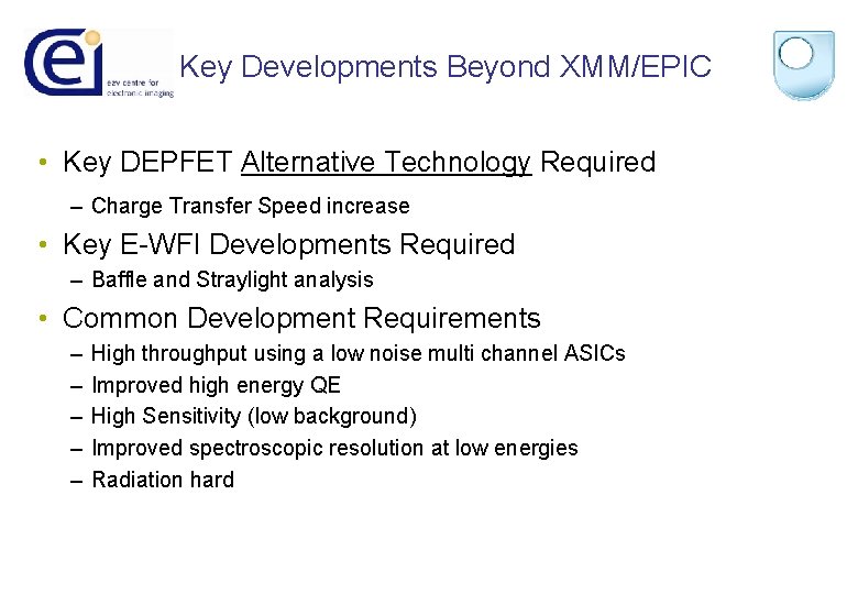
Key Developments Beyond XMM/EPIC • Key DEPFET Alternative Technology Required – Charge Transfer Speed increase • Key E-WFI Developments Required – Baffle and Straylight analysis • Common Development Requirements – – – High throughput using a low noise multi channel ASICs Improved high energy QE High Sensitivity (low background) Improved spectroscopic resolution at low energies Radiation hard

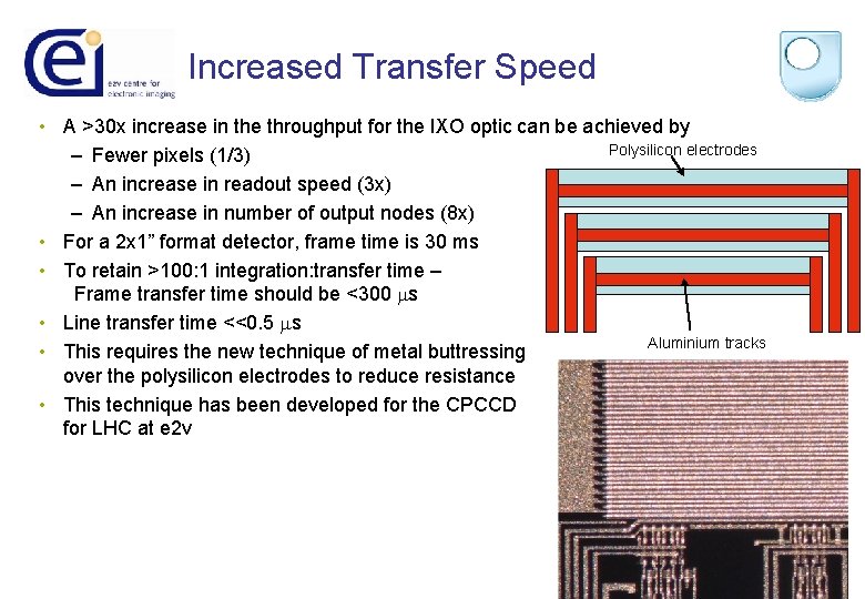
Increased Transfer Speed • A >30 x increase in the throughput for the IXO optic can be achieved by Polysilicon electrodes – Fewer pixels (1/3) – An increase in readout speed (3 x) – An increase in number of output nodes (8 x) • For a 2 x 1” format detector, frame time is 30 ms • To retain >100: 1 integration: transfer time – Frame transfer time should be <300 ms • Line transfer time <<0. 5 ms Aluminium tracks • This requires the new technique of metal buttressing over the polysilicon electrodes to reduce resistance • This technique has been developed for the CPCCD for LHC at e 2 v

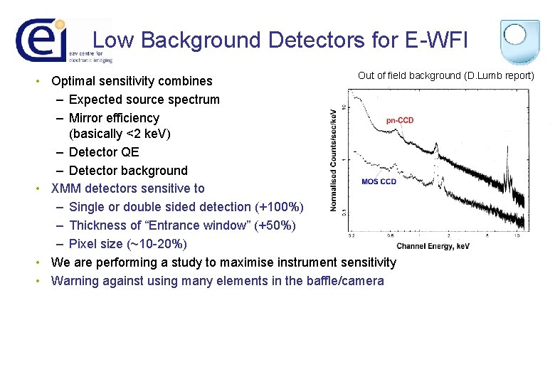
Low Background Detectors for E-WFI Out of field background (D. Lumb report) • Optimal sensitivity combines – Expected source spectrum – Mirror efficiency (basically <2 ke. V) – Detector QE – Detector background • XMM detectors sensitive to – Single or double sided detection (+100%) – Thickness of “Entrance window” (+50%) – Pixel size (~10 -20%) • We are performing a study to maximise instrument sensitivity • Warning against using many elements in the baffle/camera

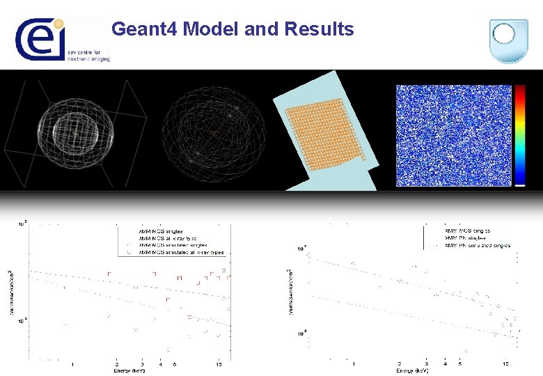
Energy Geant 4 Model and Results

Instrument Background Study • Extensive study performed using Geant-4 comparing to EPIC MOS+pn, Suzaku and Swift instruments • For XMM EPIC the dominant background is LE electrons from the camera – EPIC array averaged area to primary protons ~14 cm 2, ~50/s, >99. 9% penetrating particles rejected – Residual background from soft electrons from surroundings plus Compton electrons internal to sensor – With scintillator veto shield, averaged area >300 cm 2, ~ 1200/s, would add to dead time, high-Z would also create more gamma background • FI MOS CCDs inherently lower sensitivity to these than fully depleted BI structures • Need to perform study into reducing the electron component off the shield • Further Geant-4 model development to be undertaken • Concerns over high-Z active shields impacting Si background + coatings – EPIC used Al shielding specifically to minimise background

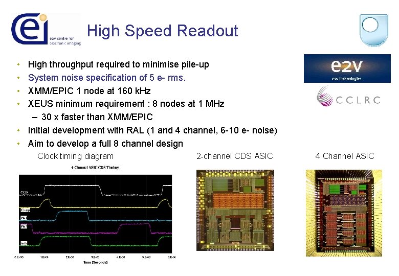
High Speed Readout • • High throughput required to minimise pile-up System noise specification of 5 e- rms. XMM/EPIC 1 node at 160 k. Hz XEUS minimum requirement : 8 nodes at 1 MHz – 30 x faster than XMM/EPIC • Initial development with RAL (1 and 4 channel, 6 -10 e- noise) • Aim to develop a full 8 channel design Clock timing diagram 2 -channel CDS ASIC 4 Channel ASIC

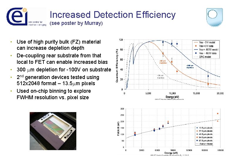
Increased Detection Efficiency (see poster by Murray) • Use of high purity bulk (FZ) material can increase depletion depth • De-coupling rear substrate from that local to FET can enable increased bias • 300 mm depletion for -100 V on substrate • 2 nd generation devices tested using 512 x 2048 format – 13. 5 mm pixels • Used on-chip binning to explore FWHM resolution vs. pixel size ~93 µm depletion ~295 µm depletion ~35 µm depletion CCD 247 Quantum Efficiency Measurements CCD 247 Spectral Resolution Measurements (VSS = -100 V)

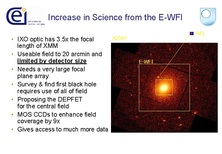
Increase in Science from the E-WFI • IXO optic has 3. 5 x the focal length of XMM • Useable field to 20 arcmin and limited by detector size • Needs a very large focal plane array • Survey & find first black hole requires use of all of field • Proposing the DEPFET for the central field • MOS CCDs to enhance field coverage by 9 x • Gives access to much more data NFI A 2597 E-WFI

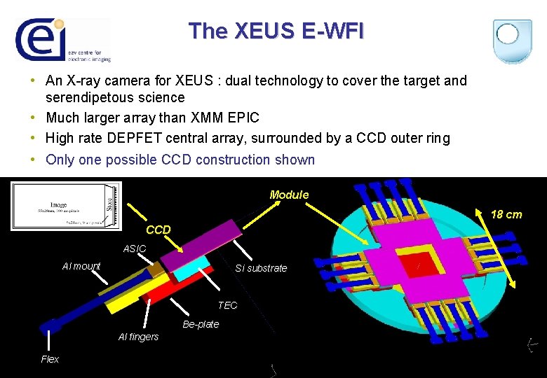
The XEUS E-WFI • An X-ray camera for XEUS : dual technology to cover the target and serendipetous science • Much larger array than XMM EPIC • High rate DEPFET central array, surrounded by a CCD outer ring • Only one possible CCD construction shown Module 18 cm CCD ASIC Al mount Si substrate TEC Be-plate Al fingers Flex

The Swept Charge Device • Non-imaging CCD-based sensor for XRF • Developed under the UK Impact programme ~1998 • New generation of devices designed in 2007

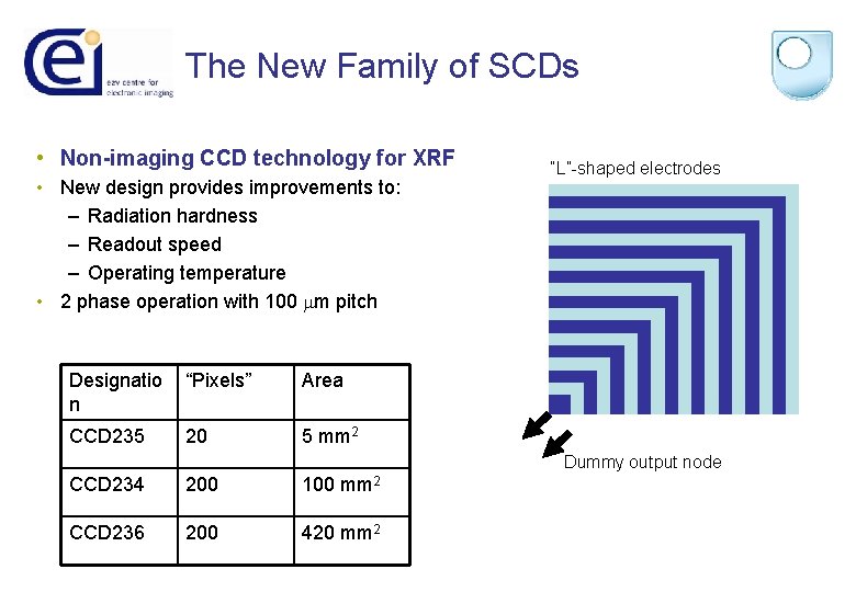
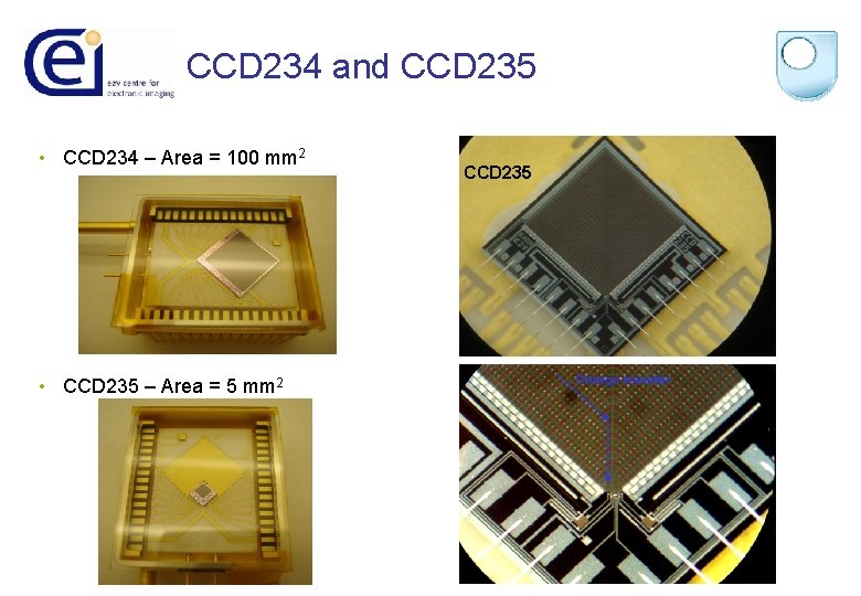
The New Family of SCDs • Non-imaging CCD technology for XRF • New design provides improvements to: – Radiation hardness – Readout speed – Operating temperature • 2 phase operation with 100 mm pitch Designatio n “Pixels” Area CCD 235 20 5 mm 2 “L”-shaped electrodes Dummy output node CCD 234 200 100 mm 2 CCD 236 200 420 mm 2

CCD 234 and CCD 235 • CCD 234 – Area = 100 mm 2 • CCD 235 – Area = 5 mm 2 CCD 235

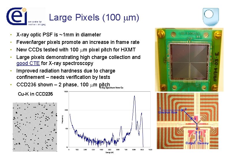
Large Pixels (100 mm) • • X-ray optic PSF is ~1 mm in diameter Fewer/larger pixels promote an increase in frame rate New CCDs tested with 100 mm pixel pitch for HXMT Large pixels demonstrating high charge collection and good CTE for X-ray spectroscopy • Improved radiation hardness due to charge confinement – needs verification by tests • CCD 236 shown – 2 phase, 100 mm pitch Cu-K in CCD 235

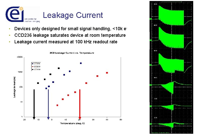
Leakage Current • Devices only designed for small signal handling, <10 k e • CCD 236 leakage saturates device at room temperature • Leakage current measured at 100 k. Hz readout rate

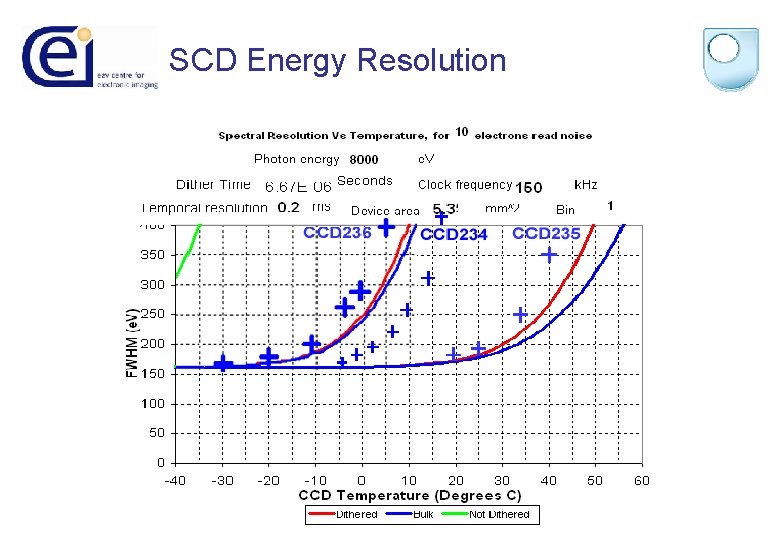
SCD Energy Resolution

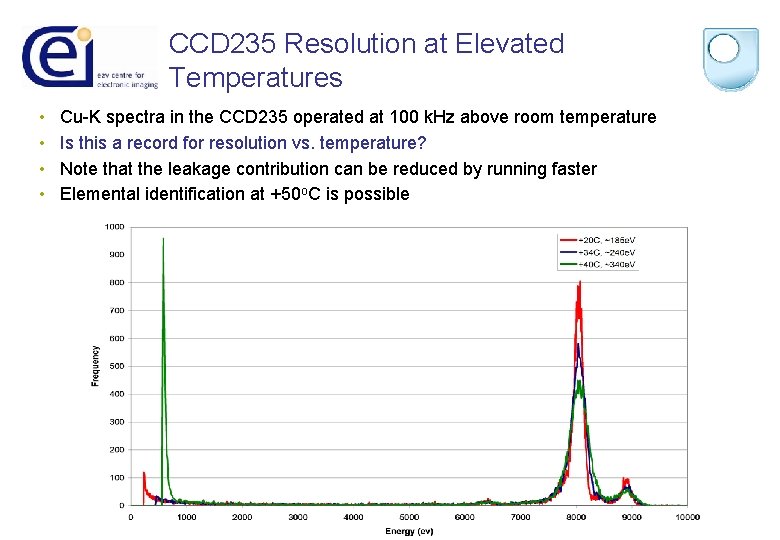
CCD 235 Resolution at Elevated Temperatures • • Cu-K spectra in the CCD 235 operated at 100 k. Hz above room temperature Is this a record for resolution vs. temperature? Note that the leakage contribution can be reduced by running faster Elemental identification at +50 o. C is possible

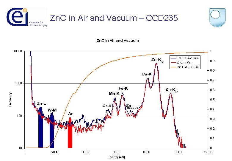
Zn. O in Air and Vacuum – CCD 235

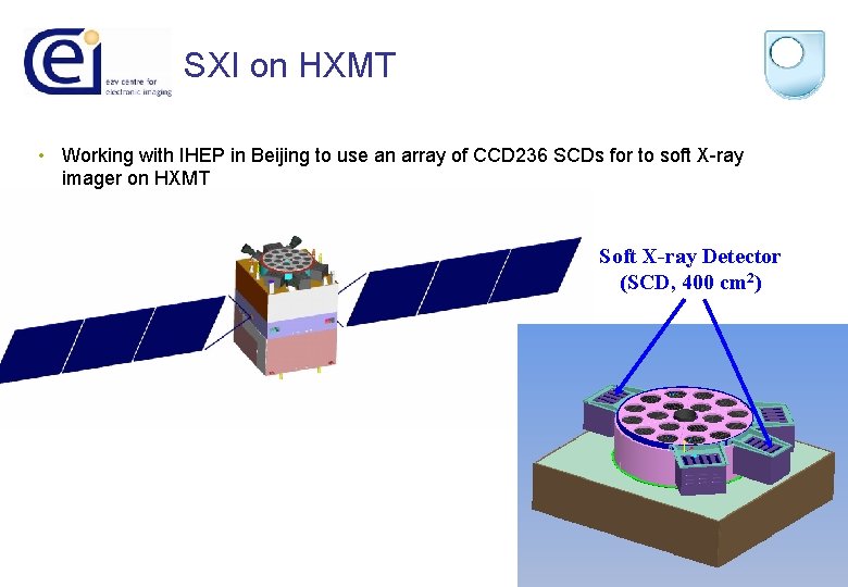
SXI on HXMT • Working with IHEP in Beijing to use an array of CCD 236 SCDs for to soft X-ray imager on HXMT • Detector area = 320 cm 2 Soft X-ray Detector (SCD, 400 cm 2)

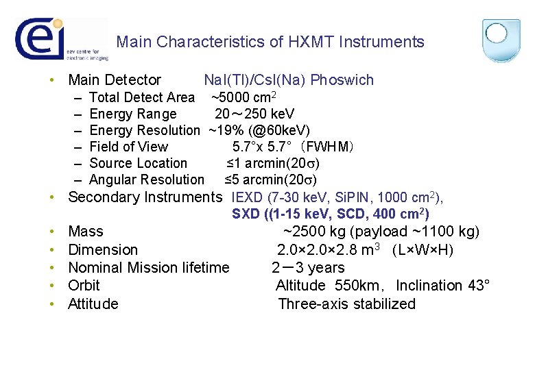
Main Characteristics of HXMT Instruments • Main Detector Na. I(Tl)/Cs. I(Na) Phoswich – – – Total Detect Area ~5000 cm 2 Energy Range 20~ 250 ke. V Energy Resolution ~19% (@60 ke. V) Field of View 5. 7°x 5. 7°(FWHM) Source Location ≤ 1 arcmin(20 ) Angular Resolution ≤ 5 arcmin(20 ) • Secondary Instruments IEXD (7 -30 ke. V, Si. PIN, 1000 cm 2), SXD ((1 -15 ke. V, SCD, 400 cm 2) • • • Mass Dimension Nominal Mission lifetime Orbit Attitude ~2500 kg (payload ~1100 kg) 2. 0× 2. 8 m 3 (L×W×H) 2-3 years Altitude 550 km,Inclination 43° Three-axis stabilized

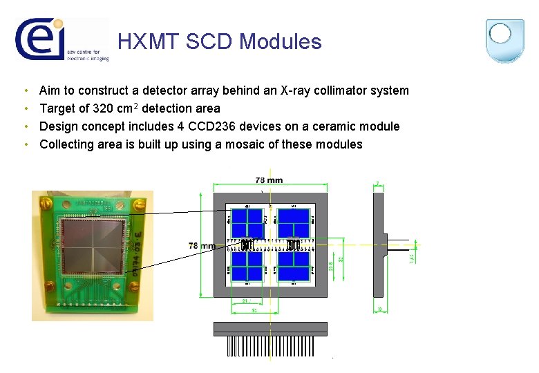
HXMT SCD Modules • • Aim to construct a detector array behind an X-ray collimator system Target of 320 cm 2 detection area Design concept includes 4 CCD 236 devices on a ceramic module Collecting area is built up using a mosaic of these modules

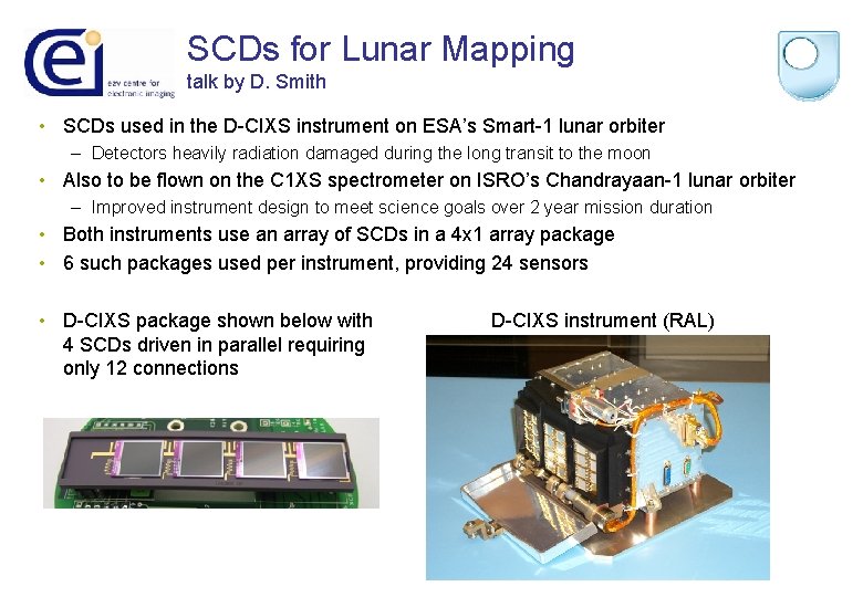
SCDs for Lunar Mapping talk by D. Smith • SCDs used in the D-CIXS instrument on ESA’s Smart-1 lunar orbiter – Detectors heavily radiation damaged during the long transit to the moon • Also to be flown on the C 1 XS spectrometer on ISRO’s Chandrayaan-1 lunar orbiter – Improved instrument design to meet science goals over 2 year mission duration • Both instruments use an array of SCDs in a 4 x 1 array package • 6 such packages used per instrument, providing 24 sensors • D-CIXS package shown below with 4 SCDs driven in parallel requiring only 12 connections D-CIXS instrument (RAL)

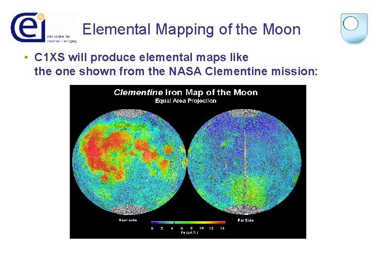
Elemental Mapping of the Moon • C 1 XS will produce elemental maps like the one shown from the NASA Clementine mission:

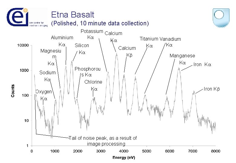
Etna Basalt (Polished, 10 minute data collection) Potassium Calcium Ka Aluminium Titanium Vanadium Ka Ka Ka Silicon Ka Calcium Magnesiu Ka Kb Manganese m Ka Ka Iron Ka Phosphorou Sodium s Ka Ka Chlorine Iron Kb Ka Oxygen Ka Tail of noise peak, as a result of image processing

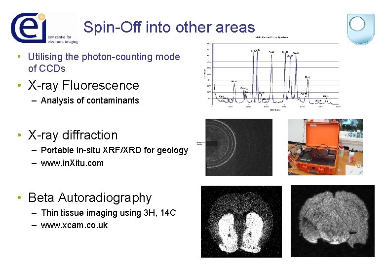
Spin-Off into other areas • Utilising the photon-counting mode of CCDs • X-ray Fluorescence – Analysis of contaminants • X-ray diffraction – Portable in-situ XRF/XRD for geology – www. in. Xitu. com • Beta Autoradiography – Thin tissue imaging using 3 H, 14 C – www. xcam. co. uk

Conclusions • MOS CCDs are being developed for future X-ray instruments in space science • Over the next year the IXO baseline configuration is likely to change (watch this space…) • Development of critical technology components is being addressed – Readout ASICs – Transfer time – Increased QE – Large pixels • Currently no funding for a single demonstrator model incorporating all elements • Modelling of instrument background is identifying the key contributors to aid their reduction in XEUS • SCD technology is being applied to XRF for elemental mapping for Lunar science • Spin-off is occurring into terrestrial XRF, XRD and Beta Autoradiography