XFEL 2 D Pixel Clock and Control System
- Slides: 14

XFEL 2 D Pixel Clock and Control System Train Builder Meeting, UCL 11 May 2010 Erdem Motuk, Martin Postranecky, Matt Warren, Matthew Wing, C+C

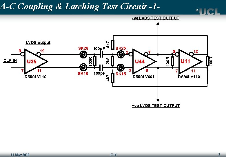
A-C Coupling & Latching Test Circuit -1 - 11 DS 90 LV 110 SK 16 SK 25 2 100 p. F U 44 SK 15 8 7 3 12 6 DS 90 LV 001 U 11 7 100 R U 35 7 100 p. F 2 k 2 CLK IN SK 26 4 k 7 12 100 R 8 100 R LVDS output 4 k 7 -ve LVDS TEST OUTPUT 11 DS 90 LV 110 +ve LVDS TEST OUTPUT 11 May 2010 C+C 2

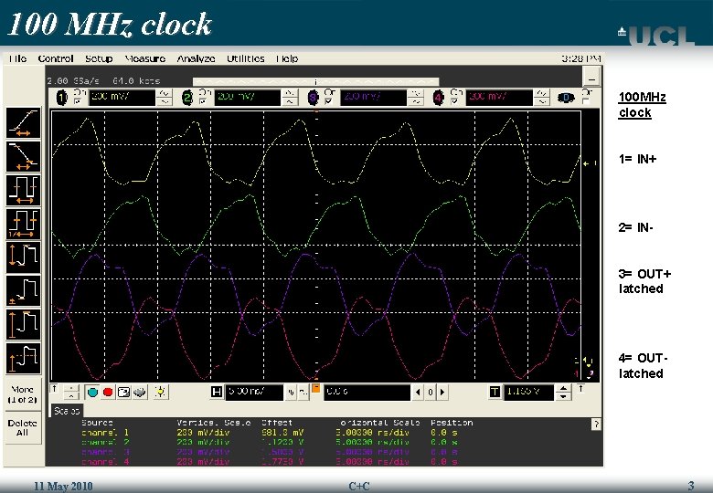
100 MHz clock 100 MHz clock 1= IN+ 2= IN 3= OUT+ latched 4= OUTlatched 11 May 2010 C+C 3

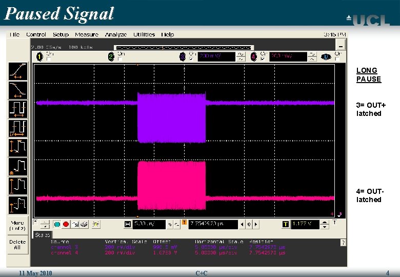
Paused Signal LONG PAUSE 3= OUT+ latched 4= OUTlatched 11 May 2010 C+C 4

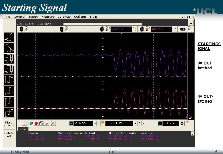
Starting Signal STARTINGS IGNAL 3= OUT+ latched 4= OUTlatched 11 May 2010 C+C 5

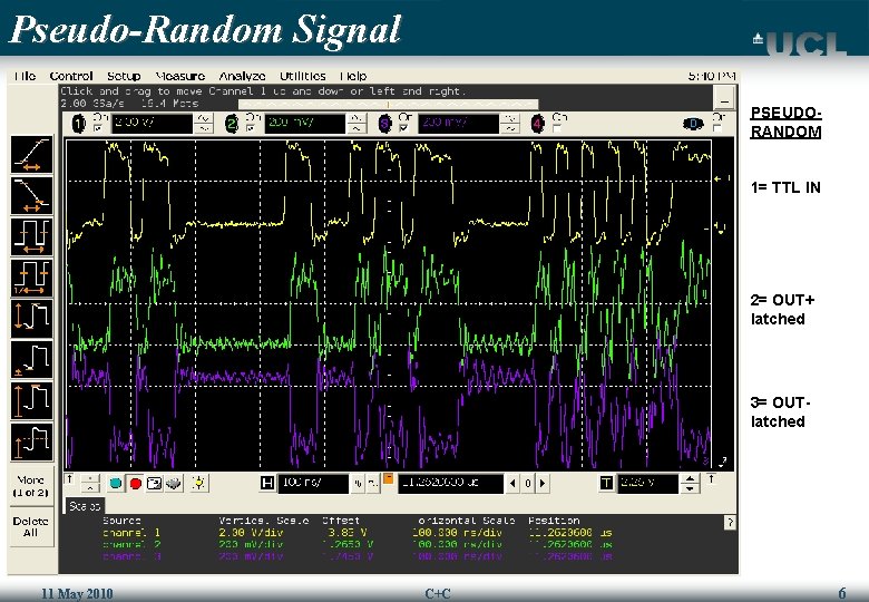
Pseudo-Random Signal PSEUDORANDOM 1= TTL IN 2= OUT+ latched 3= OUTlatched 11 May 2010 C+C 6

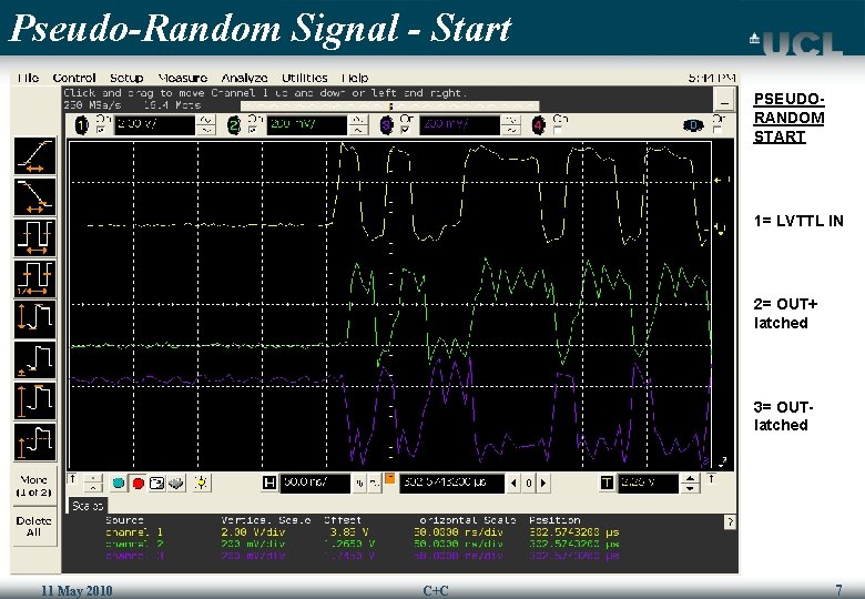
Pseudo-Random Signal - Start PSEUDORANDOM START 1= LVTTL IN 2= OUT+ latched 3= OUTlatched 11 May 2010 C+C 7

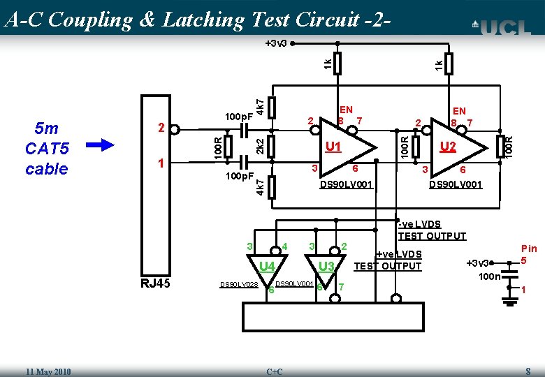
A-C Coupling & Latching Test Circuit -2 - 3 DS 90 LV 028 6 4 3 6 2 U 3 DS 90 LV 001 C+C 6 7 U 2 3 DS 90 LV 001 U 4 11 May 2010 1 k U 1 3 RJ 45 2 100 R 2 k 2 100 p. F EN 8 7 100 R 1 EN 8 7 2 4 k 7 2 100 R 5 m CAT 5 cable 100 p. F 4 k 7 1 k +3 v 3 6 DS 90 LV 001 -ve LVDS TEST OUTPUT +3 v 3 100 n Pin 5 1 8

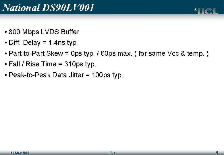
National DS 90 LV 001 • 800 Mbps LVDS Buffer • Diff. Delay = 1. 4 ns typ. • Part-to-Part Skew = 0 ps typ. / 60 ps max. ( for same Vcc & temp. ) • Fall / Rise Time = 310 ps typ. • Peak-to-Peak Data Jitter = 100 ps typ. 11 May 2010 C+C 9

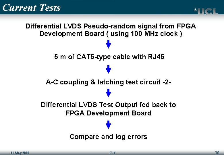
Current Tests Differential LVDS Pseudo-random signal from FPGA Development Board ( using 100 MHz clock ) 5 m of CAT 5 -type cable with RJ 45 A-C coupling & latching test circuit -2 Differential LVDS Test Output fed back to FPGA Development Board Compare and log errors 11 May 2010 C+C 10

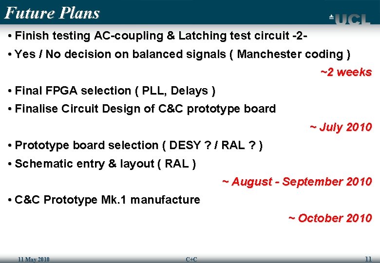
Future Plans • Finish testing AC-coupling & Latching test circuit -2 • Yes / No decision on balanced signals ( Manchester coding ) ~2 weeks • Final FPGA selection ( PLL, Delays ) • Finalise Circuit Design of C&C prototype board ~ July 2010 • Prototype board selection ( DESY ? / RAL ? ) • Schematic entry & layout ( RAL ) ~ August - September 2010 • C&C Prototype Mk. 1 manufacture ~ October 2010 11 May 2010 C+C 11

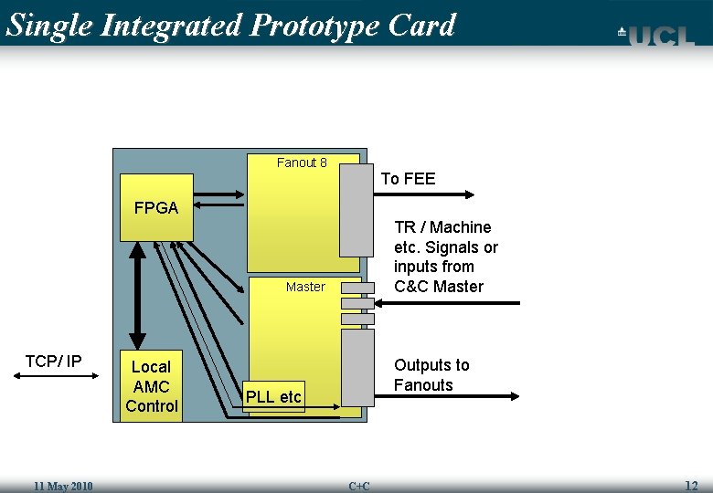
Single Integrated Prototype Card Fanout 8 To FEE FPGA TR / Machine etc. Signals or inputs from C&C Master TCP/ IP 11 May 2010 Local AMC Control Outputs to Fanouts PLL etc C+C 12

End…. . 11 May 2010 C+C 13

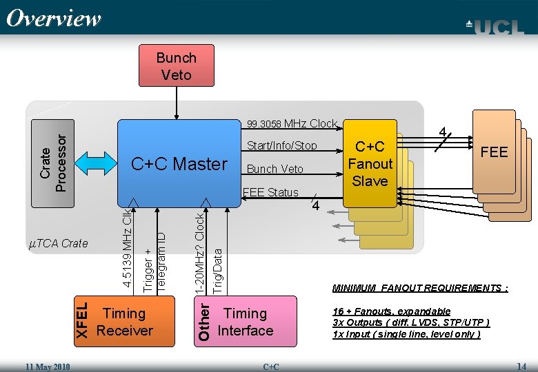
Overview Bunch Veto Crate Processor 99. 3058 MHz Clock Start/Info/Stop C+C Master Trig/Data 1 -20 MHz? Clock Trigger + Telegram ID Timing Receiver Other XFEL 4. 5139 MHz Clk FEE Status μTCA Crate 11 May 2010 Bunch Veto C+C Fanout Slave C+C Fanout 4 FEE FEE C+C Fanout 4 C+C Fanout MINIMUM FANOUT REQUIREMENTS : Timing Interface C+C 16 + Fanouts, expandable 3 x Outputs ( diff. LVDS, STP/UTP ) 1 x Input ( single line, level only ) 14