www seattlenano org Nanotechnology Characterization SHINE Seattles Hub

www. seattlenano. org Nanotechnology Characterization SHINE: Seattle’s Hub for Industry-driven Nanotechnology Education
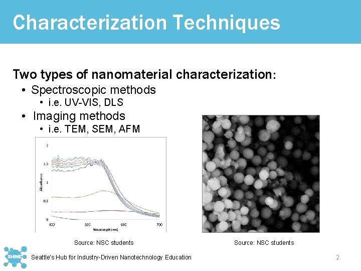
Characterization Techniques Two types of nanomaterial characterization: • Spectroscopic methods • i. e. UV-VIS, DLS • Imaging methods • i. e. TEM, SEM, AFM Source: NSC students Seattle’s Hub for Industry-Driven Nanotechnology Education Source: NSC students 2
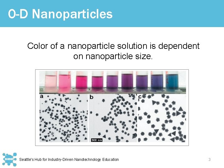
0 -D Nanoparticles Color of a nanoparticle solution is dependent on nanoparticle size. Seattle’s Hub for Industry-Driven Nanotechnology Education 3
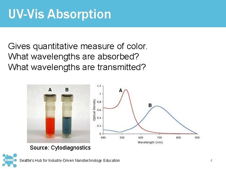
UV-Vis Absorption Gives quantitative measure of color. What wavelengths are absorbed? What wavelengths are transmitted? Source: Cytodiagnostics Seattle’s Hub for Industry-Driven Nanotechnology Education 4
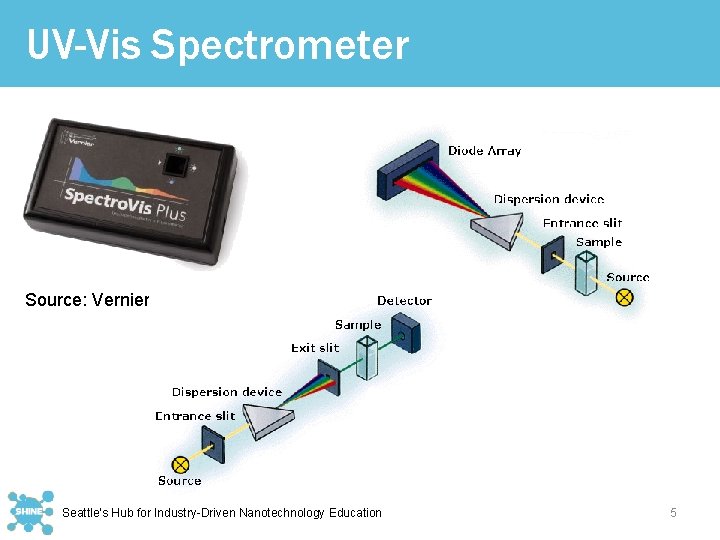
UV-Vis Spectrometer Source: Vernier Seattle’s Hub for Industry-Driven Nanotechnology Education 5
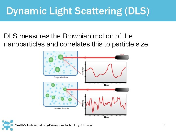
Dynamic Light Scattering (DLS) DLS measures the Brownian motion of the nanoparticles and correlates this to particle size Seattle’s Hub for Industry-Driven Nanotechnology Education 6
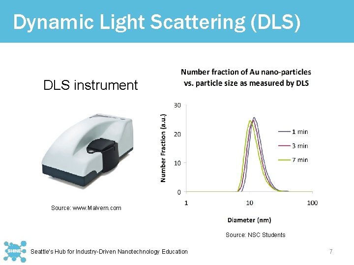
Dynamic Light Scattering (DLS) DLS instrument Source: www. Malvern. com Source: NSC Students Seattle’s Hub for Industry-Driven Nanotechnology Education 7
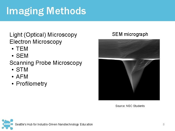
Imaging Methods Light (Optical) Microscopy Electron Microscopy • TEM • SEM Scanning Probe Microscopy • STM • AFM • Profilometry SEM micrograph Source: NSC Students Seattle’s Hub for Industry-Driven Nanotechnology Education 8
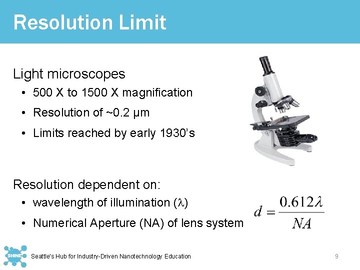
Resolution Limit Light microscopes • 500 X to 1500 X magnification • Resolution of ~0. 2 µm • Limits reached by early 1930’s Resolution dependent on: • wavelength of illumination ( ) • Numerical Aperture (NA) of lens system Seattle’s Hub for Industry-Driven Nanotechnology Education 9
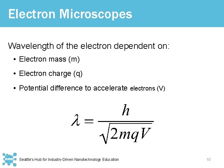
Electron Microscopes Wavelength of the electron dependent on: • Electron mass (m) • Electron charge (q) • Potential difference to accelerate electrons (V) Seattle’s Hub for Industry-Driven Nanotechnology Education 10
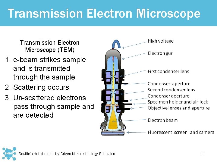
Transmission Electron Microscope (TEM) 1. e-beam strikes sample and is transmitted through the sample 2. Scattering occurs 3. Un-scattered electrons pass through sample and are detected Seattle’s Hub for Industry-Driven Nanotechnology Education 11
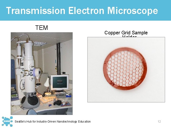
Transmission Electron Microscope TEM Seattle’s Hub for Industry-Driven Nanotechnology Education Copper Grid Sample Holder 12
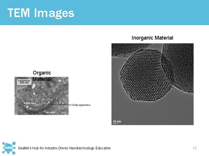
TEM Images Inorganic Material Organic Material Seattle’s Hub for Industry-Driven Nanotechnology Education 13
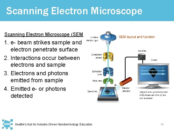
Scanning Electron Microscope (SEM) 1. e- beam strikes sample and electron penetrate surface 2. Interactions occur between electrons and sample 3. Electrons and photons emitted from sample 4. Emitted e- or photons detected Seattle’s Hub for Industry-Driven Nanotechnology Education 14
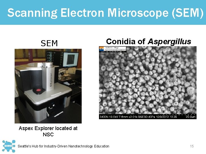
Scanning Electron Microscope (SEM) SEM Conidia of Aspergillus Aspex Explorer located at NSC Seattle’s Hub for Industry-Driven Nanotechnology Education 15
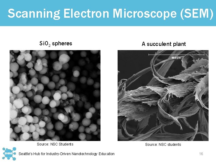
Scanning Electron Microscope (SEM) Si. O 2 spheres A succulent plant Source: NSC Students Source: NSC students Seattle’s Hub for Industry-Driven Nanotechnology Education 16
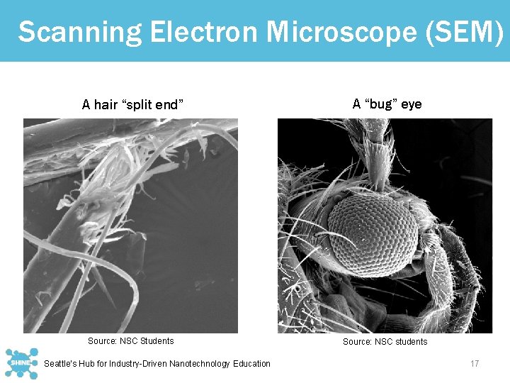
Scanning Electron Microscope (SEM) A hair “split end” A “bug” eye Source: NSC Students Source: NSC students Seattle’s Hub for Industry-Driven Nanotechnology Education 17
Scanning Probe Microscopy Measure feedback from atomically defined tip Many types of feedback (dependent on tip) AFM – Forces between sample and tip STM – Tunneling current between sample and tip Seattle’s Hub for Industry-Driven Nanotechnology Education 18
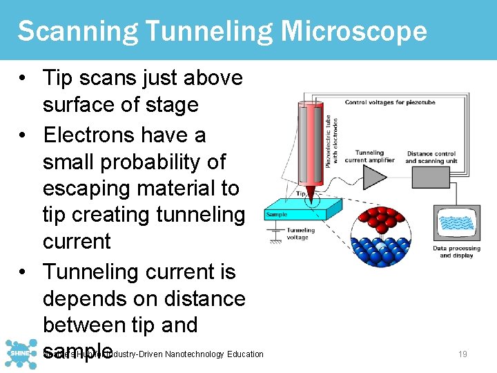
Scanning Tunneling Microscope • Tip scans just above surface of stage • Electrons have a small probability of escaping material to tip creating tunneling current • Tunneling current is depends on distance between tip and sample Seattle’s Hub for Industry-Driven Nanotechnology Education 19
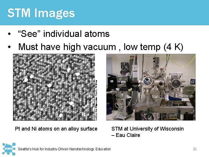
STM Images • “See” individual atoms • Must have high vacuum , low temp (4 K) Pt and Ni atoms on an alloy surface Seattle’s Hub for Industry-Driven Nanotechnology Education STM at University of Wisconsin – Eau Claire 20
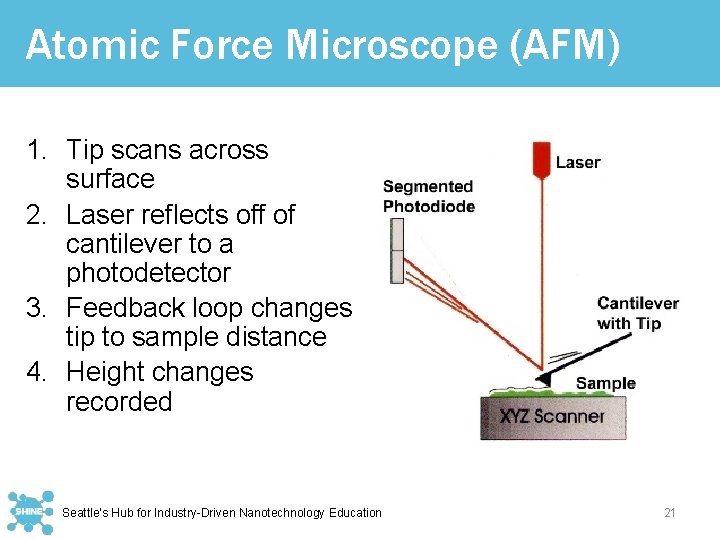
Atomic Force Microscope (AFM) 1. Tip scans across surface 2. Laser reflects off of cantilever to a photodetector 3. Feedback loop changes tip to sample distance 4. Height changes recorded Seattle’s Hub for Industry-Driven Nanotechnology Education 21
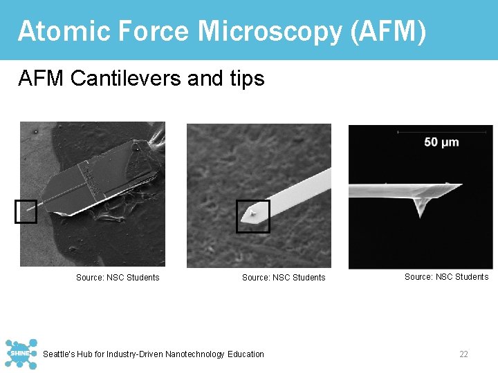
Atomic Force Microscopy (AFM) AFM Cantilevers and tips Source: NSC Students Seattle’s Hub for Industry-Driven Nanotechnology Education Source: NSC Students 22
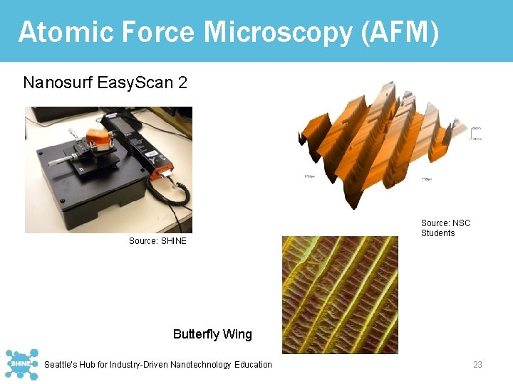
Atomic Force Microscopy (AFM) Nanosurf Easy. Scan 2 Source: SHINE Source: NSC Students Butterfly Wing Seattle’s Hub for Industry-Driven Nanotechnology Education 23
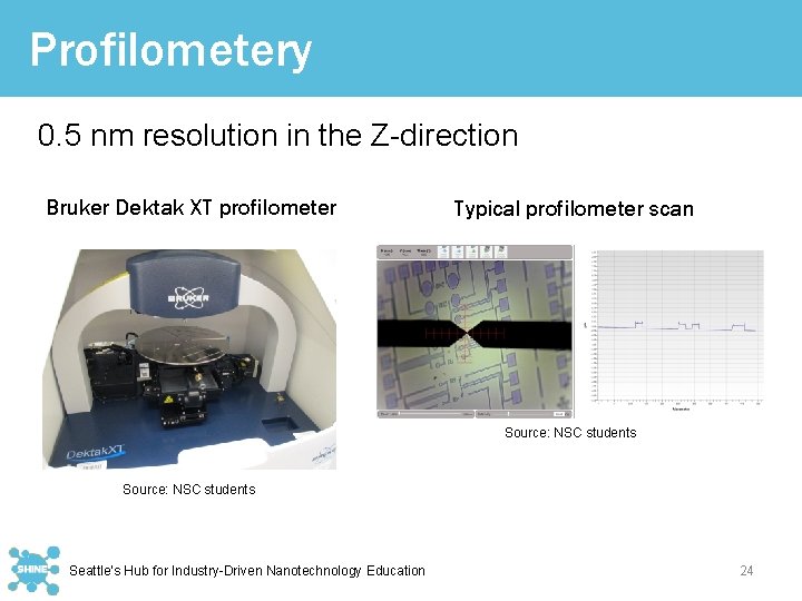
Profilometery 0. 5 nm resolution in the Z-direction Bruker Dektak XT profilometer Typical profilometer scan Source: NSC students Seattle’s Hub for Industry-Driven Nanotechnology Education 24
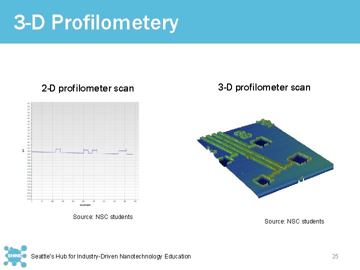
3 -D Profilometery 2 -D profilometer scan Source: NSC students Seattle’s Hub for Industry-Driven Nanotechnology Education 3 -D profilometer scan Source: NSC students 25
Image References Slide 3 Adv. Mater. 2006. , 18, 2529 - 2534 Slide 4 Gold nanoparticle shape dependent LSPR. Cytodiagnostics. [Online Image]. 8 May 2016. <http: //www. cytodiagnostics. com/store/pc/Introduction-to-Gold -Nanoparticle-Characterization-d 3. htm> Spectra. Vis Plus Spectrophotometer. Vernier. [Online Image]. 8 May 2016. <http: //www. vernier. com/products/sensors/spectrometers/visible-range/svis -pl/> Slide 5 Slide 6 Spectrometer Diagrams. Adapted from Hewlett-Packard's "Fundamentals of Modern UV-Visible Spectroscopy" publication number 12 -5965 -512 E, 1996. [Online Image]. 8 May 2016 <http: //www. thescientist. com/? articles. view/article. No/18797/title/Across-the-Spectrum-Instrumentation-for-UV-Vis-Spectrophotometry/> Dynamic Light Scattering. Jones, Mike. [Online Image]. 21 June 2016. <https: //commons. wikimedia. org/wiki/File: DLS. svg> Seattle’s Hub for Industry-Driven Nanotechnology Education 26
![Image References Intensity Fluctuations and Brownian Motion. AZO Materials. [Online Image] 10 May 2016. Image References Intensity Fluctuations and Brownian Motion. AZO Materials. [Online Image] 10 May 2016.](http://slidetodoc.com/presentation_image_h/dccffc108fd67829a22f78b780246f5b/image-27.jpg)
Image References Intensity Fluctuations and Brownian Motion. AZO Materials. [Online Image] 10 May 2016. <http: //www. azom. com/article. aspx? Article. ID=12255> Slide 6 Weighted Distributions. Yilun Li. Andrew R. Barron, Dynamic Light Scattering. Open. Stax CNX. ay 014 http: //cnx. org/contents/3 fc 98 dad-934 d 45 e 6 -a 19 f-c 0 a 1 cf 440 d 43@1. > Slide 7 Microscope. [Online Image] 10 May 2016. <http: //mssmith. wicomico. wikispaces. net/Tools+Scientists+Use> Slide 11 Transmission Electron Microscope. Wikimedia Commons. [Online Image]. 10 May 2016 <https: //commons. wikimedia. org/wiki/File: Electron_Microscope. png> Seattle’s Hub for Industry-Driven Nanotechnology Education 27
Image References Slide 12 TEM. Boundless. “Electron Microscopy. ” Boundless Microbiology. Boundless, 13 Apr. 2016. Retrieved 10 May. 2016 from <https: //www. boundless. com/microbiology/textbooks/boundlessmicrobiology-textbook/microscopy-3/other-types-of-microscopy-30/electronmicroscopy-249 -1065/> 3 mm copper grid. Lilly_M. Wikimedia Commons. [Online Image]. 17 May 2016. <https: //commons. wikimedia. org/wiki/File: 3_mm_copper_grid_electron_mic roscopy_for_sample-04. jpg> Slide 13 Golgi Apparatus. [Online Image]. 17 May 2016. <https: //courses. candelalearning. com/biology 11 xmaster/chapter/eukaryotic -cells/> Mesoporous silica nanoparticle. [Online Image]. 21 May 2016. <https: //en. wikipedia. org/wiki/File: Mesopourus_silica_closeup. jpg> Slide 14 SEM Image. My. Scope. [Online Image]. 21 May 2016. <http: //li 15594. members. linode. com/myscope/sem/practice/principles/layout. php> Seattle’s Hub for Industry-Driven Nanotechnology Education 28
![Image References Slide 15 Conidium. Gans, Murray. [Online Image]. 21 May 2016. <http: //murrygans. Image References Slide 15 Conidium. Gans, Murray. [Online Image]. 21 May 2016. <http: //murrygans.](http://slidetodoc.com/presentation_image_h/dccffc108fd67829a22f78b780246f5b/image-29.jpg)
Image References Slide 15 Conidium. Gans, Murray. [Online Image]. 21 May 2016. <http: //murrygans. blogspot. com/2013_04_01_archive. html> Slide 19 Scanning Tunneling Microscope. [Online Image]. 22 May 2016. <https: //en. wikipedia. org/wiki/Scanning_tunneling_microscope#/media/File: Scanning. Tunneling. Microscope_schematic. png> Slide 20 Slide 21 Pt and Ni. Richmond, Michael. [Online Image]. 22 May 2016. <http: //spiff. rit. edu/classes/phys 314/lectures/stm. html> STM. [Online Image]. 22 May 2016. <http: //www. uwec. edu/Matsci/center/instrumentation/> AFM. Hansma, Helen. [Online Image]. 22 May 2016. <http: //web. physics. ucsb. edu/~hhansma/biomolecules. htm> Seattle’s Hub for Industry-Driven Nanotechnology Education 29
![Image References Slide 22 Butterfly Wing. Nano. Surf. [Online Image]. 22 May 2016. <https: Image References Slide 22 Butterfly Wing. Nano. Surf. [Online Image]. 22 May 2016. <https:](http://slidetodoc.com/presentation_image_h/dccffc108fd67829a22f78b780246f5b/image-30.jpg)
Image References Slide 22 Butterfly Wing. Nano. Surf. [Online Image]. 22 May 2016. <https: //www. nanosurf. com/en/application/70 -butterfly-wings-a-fragilebiological-nanostructure> To access additional educational resources please visit: www. seattlenano. org This material is based upon work supported by the National Science Foundation under Grant Number 1204279. Any opinions, findings, and conclusions or recommendations expressed in this material are those of the author(s) and do not necessarily reflect the views of the National Science Foundation. 30
- Slides: 30