WP 2 ondetector power management F Faccio G
- Slides: 43

WP 2: on-detector power management F. Faccio, G. Blanchot, S. Michelis, S. Orlandi, C. Fuentes, B. Allongue CERN – PH-ESE PH Theme 3 meeting November 11, 2008 CERN - PH dept – ESE group 1

Outline Introduction Ø Project structure Ø l l l Ø Working Team Communication Composition of WP 2 Technical status l l WP 2 -1 WP 2 -2 and 2 -3 Resources Ø Conclusion Ø PH Theme 3 meeting November 11, 2008 CERN - PH dept – ESE group 2

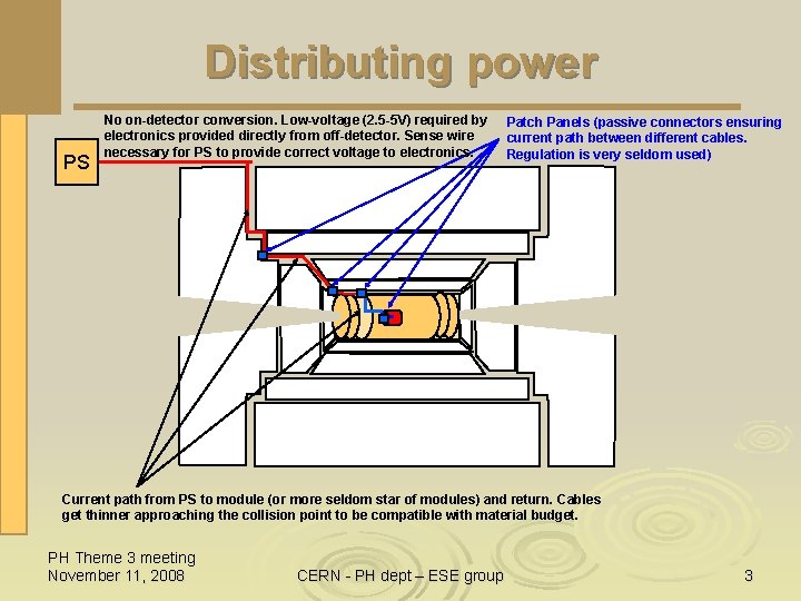
Distributing power PS No on-detector conversion. Low-voltage (2. 5 -5 V) required by electronics provided directly from off-detector. Sense wire necessary for PS to provide correct voltage to electronics. Patch Panels (passive connectors ensuring current path between different cables. Regulation is very seldom used) Current path from PS to module (or more seldom star of modules) and return. Cables get thinner approaching the collision point to be compatible with material budget. PH Theme 3 meeting November 11, 2008 CERN - PH dept – ESE group 3

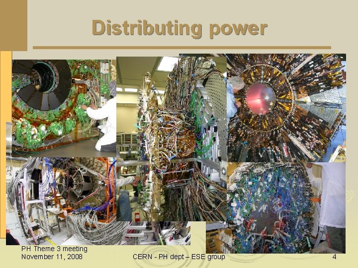
Distributing power PH Theme 3 meeting November 11, 2008 CERN - PH dept – ESE group 4

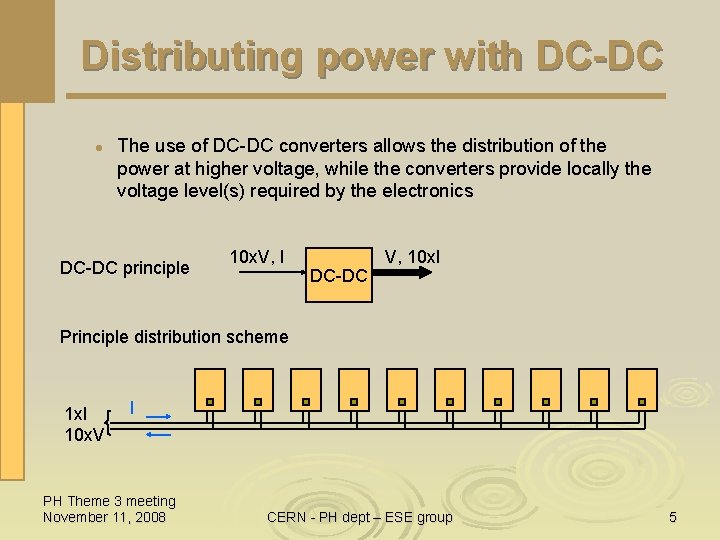
Distributing power with DC-DC l The use of DC-DC converters allows the distribution of the power at higher voltage, while the converters provide locally the voltage level(s) required by the electronics DC-DC principle 10 x. V, I DC-DC V, 10 x. I Principle distribution scheme 1 x. I 10 x. V I PH Theme 3 meeting November 11, 2008 CERN - PH dept – ESE group 5

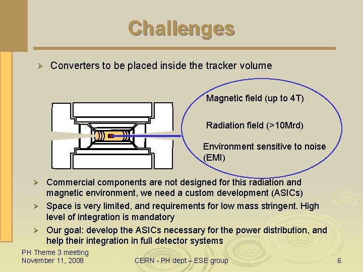
Challenges Ø Converters to be placed inside the tracker volume Magnetic field (up to 4 T) Radiation field (>10 Mrd) Environment sensitive to noise (EMI) Commercial components are not designed for this radiation and magnetic environment, we need a custom development (ASICs) Ø Space is very limited, and requirements for low mass stringent. High level of integration is mandatory Ø Our goal: develop the ASICs necessary for the power distribution, and help their integration in full detector systems Ø PH Theme 3 meeting November 11, 2008 CERN - PH dept – ESE group 6

Outline Introduction Ø Project structure Ø l l l Ø Working Team Communication Composition of WP 2 Technical status l l WP 2 -1 WP 2 -2 and 2 -3 Resources Ø Conclusion Ø PH Theme 3 meeting November 11, 2008 CERN - PH dept – ESE group 7

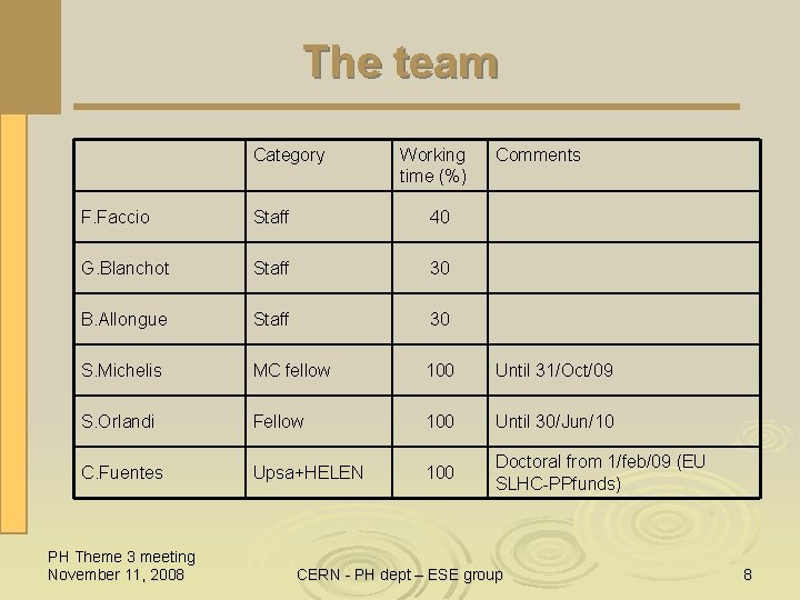
The team Category Working time (%) Comments F. Faccio Staff 40 G. Blanchot Staff 30 B. Allongue Staff 30 S. Michelis MC fellow 100 Until 31/Oct/09 S. Orlandi Fellow 100 Until 30/Jun/10 C. Fuentes Upsa+HELEN 100 Doctoral from 1/feb/09 (EU SLHC-PPfunds) PH Theme 3 meeting November 11, 2008 CERN - PH dept – ESE group 8

Communication and coordination Ø Ø Ø In opposition to the early R&D phase of LHC, power distribution is today very fashionable l 3 Working Groups: ATLAS, CMS, “common” l CMS task force (first meeting today) l Separate sessions at TWEPP, ATLAS and CMS upgrade workshops, ACES l SLHC-PP within FP 7 Parallel activities on other distribution schemes (serial powering) or different conversion approaches exist Expectations of the community are high (and impatient – maybe unnecessarily…) This all puts the development under constant pressure – and requires a very large amount of energy in reporting, coordination, discussions, …. Our activity is well known and reasonably well integrated in both ATLAS and CMS – and improving PH Theme 3 meeting November 11, 2008 CERN - PH dept – ESE group 9

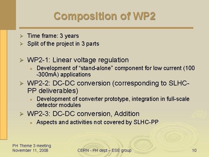
Composition of WP 2 Time frame: 3 years Ø Split of the project in 3 parts Ø Ø WP 2 -1: Linear voltage regulation l Ø WP 2 -2: DC-DC conversion (corresponding to SLHCPP deliverables) l Ø Development of “stand-alone” component for low current (100 -300 m. A) applications Development of converter prototype, integration in full-scale detector modules WP 2 -3: DC-DC conversion, Addition l Aspects and activities not covered by SLHC-PP PH Theme 3 meeting November 11, 2008 CERN - PH dept – ESE group 10

Outline Introduction Ø Project structure Ø l l l Ø Working Team Communication Composition of WP 2 Technical status l l WP 2 -1 WP 2 -2 and 2 -3 Resources Ø Conclusion Ø PH Theme 3 meeting November 11, 2008 CERN - PH dept – ESE group 11

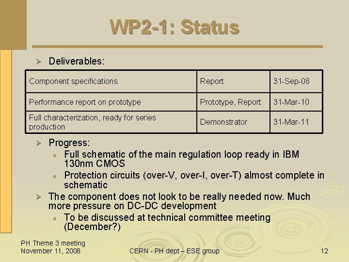
WP 2 -1: Status Ø Deliverables: Component specifications Report 31 -Sep-08 Performance report on prototype Prototype, Report 31 -Mar-10 Full characterization, ready for series production Demonstrator 31 -Mar-11 Progress: l Full schematic of the main regulation loop ready in IBM 130 nm CMOS l Protection circuits (over-V, over-I, over-T) almost complete in schematic Ø The component does not look to be really needed now. Much more pressure on DC-DC development l To be discussed at technical committee meeting (December? ) Ø PH Theme 3 meeting November 11, 2008 CERN - PH dept – ESE group 12

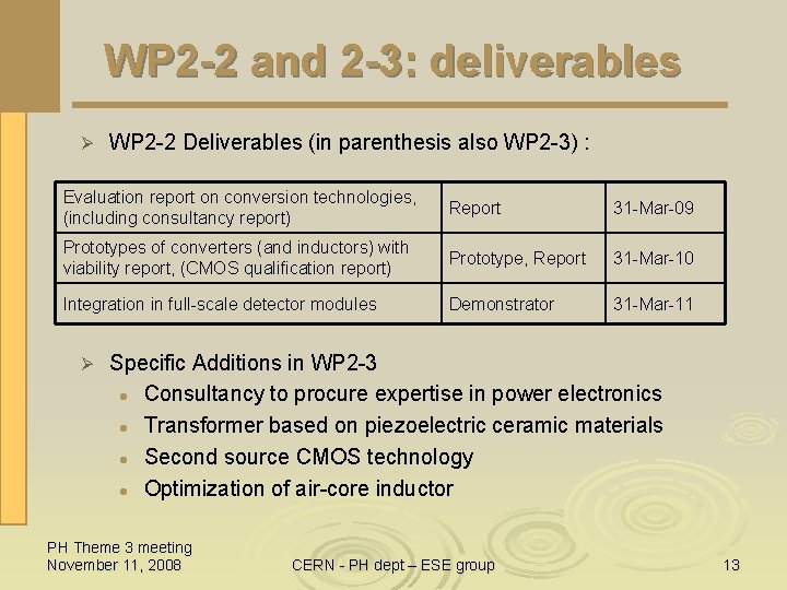
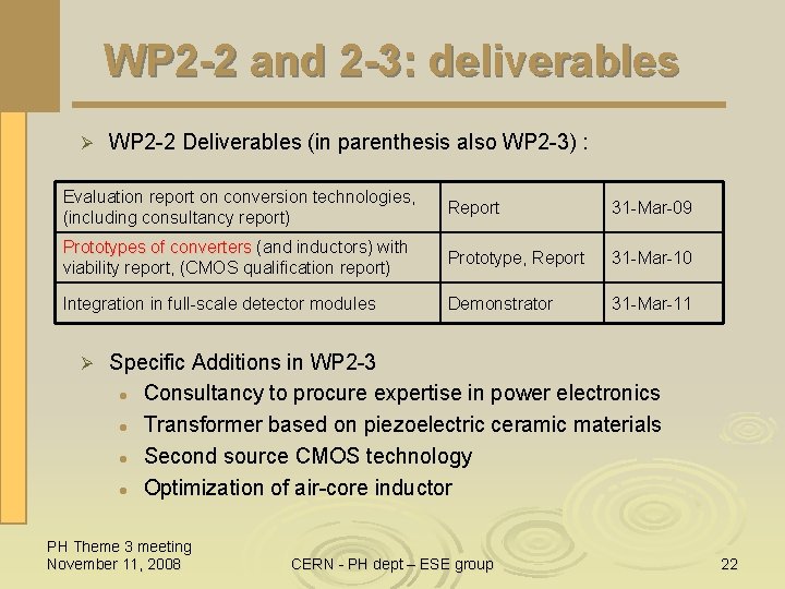
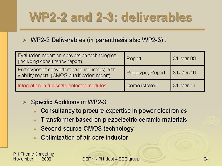
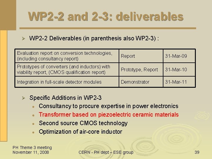
WP 2 -2 and 2 -3: deliverables Ø WP 2 -2 Deliverables (in parenthesis also WP 2 -3) : Evaluation report on conversion technologies, (including consultancy report) Report 31 -Mar-09 Prototypes of converters (and inductors) with viability report, (CMOS qualification report) Prototype, Report 31 -Mar-10 Integration in full-scale detector modules Demonstrator 31 -Mar-11 Ø Specific Additions in WP 2 -3 l Consultancy to procure expertise in power electronics l Transformer based on piezoelectric ceramic materials l Second source CMOS technology l Optimization of air-core inductor PH Theme 3 meeting November 11, 2008 CERN - PH dept – ESE group 13

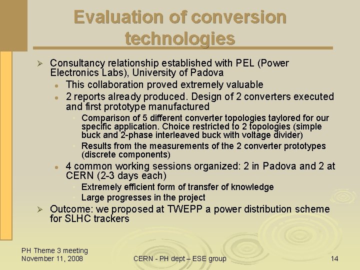
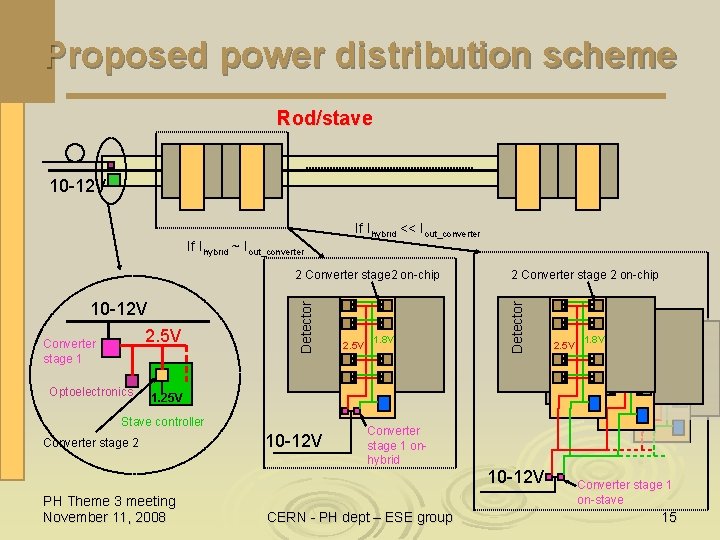
Evaluation of conversion technologies Ø Consultancy relationship established with PEL (Power Electronics Labs), University of Padova l This collaboration proved extremely valuable l 2 reports already produced. Design of 2 converters executed and first prototype manufactured • Comparison of 5 different converter topologies taylored for our specific application. Choice restricted to 2 topologies (simple buck and 2 -phase interleaved buck with voltage divider) • Results from the measurements of the 2 converter prototypes (discrete components) l 4 common working sessions organized: 2 in Padova and 2 at CERN (2 -3 days each) • Extremely efficient form of transfer of knowledge • Large progresses in the project Ø Outcome: we proposed at TWEPP a power distribution scheme for SLHC trackers PH Theme 3 meeting November 11, 2008 CERN - PH dept – ESE group 14

Proposed power distribution scheme Rod/stave 10 -12 V Optoelectronics 1. 8 V 2. 5 V Detector 2. 5 V Converter stage 1 2 Converter stage 2 on-chip Detector 10 -12 V 2 Converter stage 2 on-chip Detector If Ihybrid ~ Iout_converter If Ihybrid << Iout_converter 1. 8 V 2. 5 V 1. 8 V 1. 25 V Stave controller Converter stage 2 10 -12 V Converter stage 1 onhybrid 10 -12 V PH Theme 3 meeting November 11, 2008 CERN - PH dept – ESE group Converter stage 1 on-stave 15

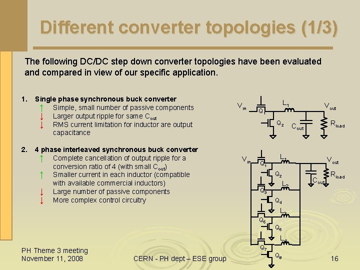
Different converter topologies (1/3) The following DC/DC step down converter topologies have been evaluated and compared in view of our specific application. 1. 2. Single phase synchronous buck converter ↑ Simple, small number of passive components ↓ Larger output ripple for same Cout ↓ RMS current limitation for inductor are output capacitance 4 phase interleaved synchronous buck converter ↑ Complete cancellation of output ripple for a conversion ratio of 4 (with small Cout) ↑ Smaller current in each inductor (compatible with available commercial inductors) ↓ Large number of passive components ↓ More complex control circuitry Vin L 1 Q 2 Vin Q 1 Vout Rload Cout L 1 Q 2 L 2 Q 3 Vout Cout Rload Q 4 L 3 Q 5 Q 6 L 4 PH Theme 3 meeting November 11, 2008 Q 7 CERN - PH dept – ESE group Q 8 16

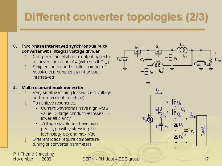
Different converter topologies (2/3) Two phase interleaved synchronous buck converter with integral voltage divider ↑ Complete cancellation of output ripple for a conversion ration of 4 (with small Cout) ↑ Simpler control and smaller number of passive components than 4 phase interleaved 4. Multi-resonant buck converter ↑ Very small switching losses (zero voltage and zero current switching) ↓ To achieve resonance: § Current waveforms have high RMS value => large conductive losses => lower efficiency § Voltage waveforms have high peaks, possibly stressing the technology beyond max Vdd ↓ Different loads require complete retuning of converter parameters PH Theme 3 meeting November 11, 2008 CERN - PH dept – ESE group ig Q 1 ir Vg C 1 Lr + Cr vr Q 2 D 1 C 2 D 2 Io + vo Load 3. 17

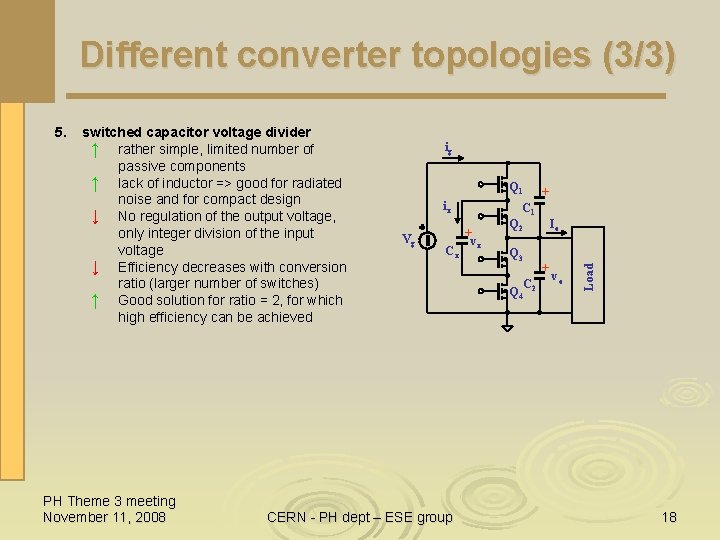
Different converter topologies (3/3) switched capacitor voltage divider ↑ rather simple, limited number of passive components ↑ lack of inductor => good for radiated noise and for compact design ↓ No regulation of the output voltage, only integer division of the input voltage ↓ Efficiency decreases with conversion ratio (larger number of switches) ↑ Good solution for ratio = 2, for which high efficiency can be achieved PH Theme 3 meeting November 11, 2008 ig Q 1 ix Vg Cx CERN - PH dept – ESE group + vx + C 1 Q 2 Q 3 C 2 Q 4 Io + vo Load 5. 18

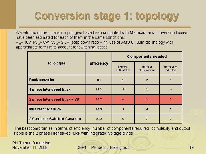
Conversion stage 1: topology Waveforms of the different topologies have been computed with Mathcad, and conversion losses have been estimated for each of them in the same conditions: Vin= 10 V, Pout= 6 W, Vout= 2. 5 V (step down ratio = 4), use of AMS 0. 18 um technology with approximate formula to account for switching losses Components needed Efficiency Topologies Number of Switches Number of Capacitors Number of Inductors 86 2 2 1 4 phase Interleaved Buck 88. 3 8 2 4 2 phase Interleaved Buck + VD 89. 7 4 3 2 Multiresonant Buck 82. 5 1 4 2 2 Cascaded Switched Capacitor 87. 3 8 7 0 Buck converter The best compromise in terms of efficiency, number of components required, complexity and output ripple is the 2 phase interleaved buck with integrated voltage divider. PH Theme 3 meeting November 11, 2008 CERN - PH dept – ESE group 19

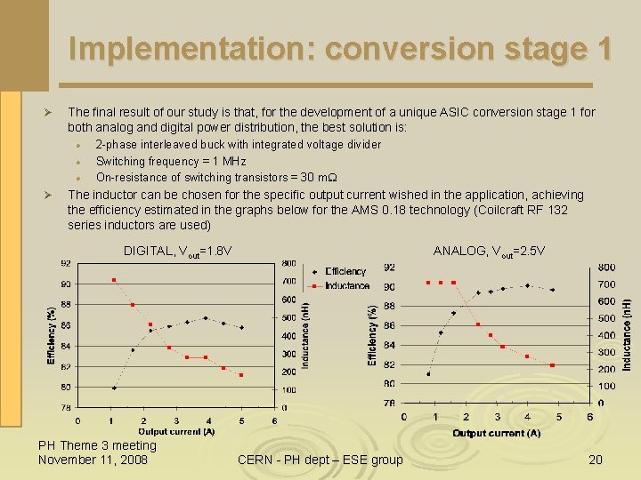
Implementation: conversion stage 1 Ø The final result of our study is that, for the development of a unique ASIC conversion stage 1 for both analog and digital power distribution, the best solution is: l l l Ø 2 -phase interleaved buck with integrated voltage divider Switching frequency = 1 MHz On-resistance of switching transistors = 30 m. W The inductor can be chosen for the specific output current wished in the application, achieving the efficiency estimated in the graphs below for the AMS 0. 18 technology (Coilcraft RF 132 series inductors are used) DIGITAL, Vout=1. 8 V PH Theme 3 meeting November 11, 2008 ANALOG, Vout=2. 5 V CERN - PH dept – ESE group 20

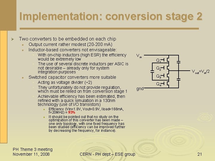
Implementation: conversion stage 2 Ø Two converters to be embedded on each chip l l Output current rather modest (20 -200 m. A) Inductor-based converters not envisageable: • With on-chip inductors (high ESR) the efficiency would be extremely low • The use of several discrete inductors per ASIC is not desirable – already only for system integration purposes l Switched capacitor converters more suitable • Acting as voltage divider (÷ 2) • They unfortunately do not provide regulation, which must be relied on from conversion stage 1 • Achievable efficiency has been estimated, then refined with a quick simulation in a 130 nm technology (use of I/O transistors) l l Vin Q 1 Q 2 Q 3 gnd Vout=Vin/2 Q 4 Efficiency (Vin=1. 8 V, Vout=0. 9 V, Iload=166 m. A, f=20 MHz) = 93% It should be pointed out that no study on the optimization of this converter has been made – one only topology, with one fixed frequency has been studied (efficiency can be improved further by decreasing the frequency, for instance). PH Theme 3 meeting November 11, 2008 CERN - PH dept – ESE group 21

WP 2 -2 and 2 -3: deliverables Ø WP 2 -2 Deliverables (in parenthesis also WP 2 -3) : Evaluation report on conversion technologies, (including consultancy report) Report 31 -Mar-09 Prototypes of converters (and inductors) with viability report, (CMOS qualification report) Prototype, Report 31 -Mar-10 Integration in full-scale detector modules Demonstrator 31 -Mar-11 Ø Specific Additions in WP 2 -3 l Consultancy to procure expertise in power electronics l Transformer based on piezoelectric ceramic materials l Second source CMOS technology l Optimization of air-core inductor PH Theme 3 meeting November 11, 2008 CERN - PH dept – ESE group 22

Prototype of converters Ø Several prototype converters using discrete components have been manufactured l Ø Main objective: study EMC First integrated prototype developed and manufactured in a CMOS 0. 35 um technology with high-V module PH Theme 3 meeting November 11, 2008 CERN - PH dept – ESE group 23

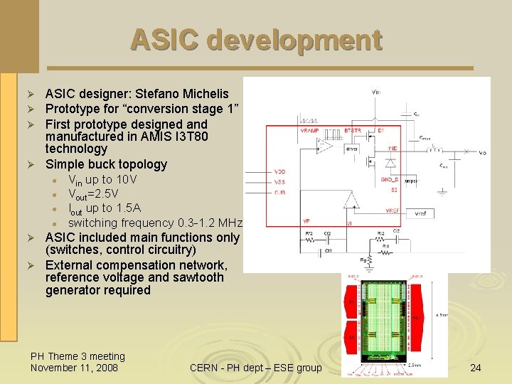
ASIC development ASIC designer: Stefano Michelis Prototype for “conversion stage 1” First prototype designed and manufactured in AMIS I 3 T 80 technology Ø Simple buck topology Ø Ø Ø l l Vin up to 10 V Vout=2. 5 V Iout up to 1. 5 A switching frequency 0. 3 -1. 2 MHz ASIC included main functions only (switches, control circuitry) Ø External compensation network, reference voltage and sawtooth generator required Ø PH Theme 3 meeting November 11, 2008 CERN - PH dept – ESE group 24

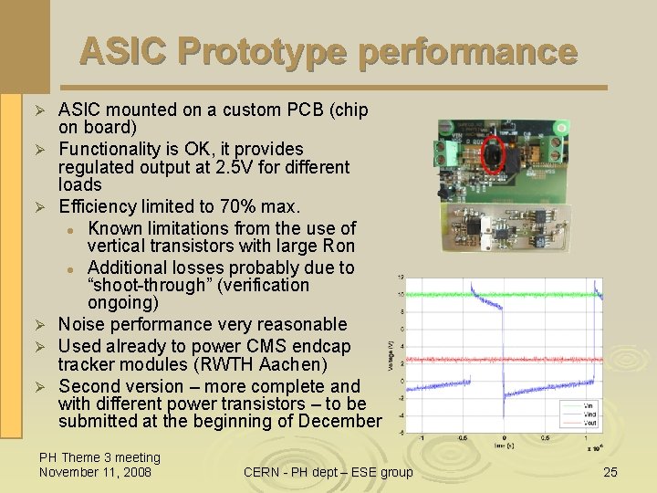
ASIC Prototype performance Ø Ø Ø ASIC mounted on a custom PCB (chip on board) Functionality is OK, it provides regulated output at 2. 5 V for different loads Efficiency limited to 70% max. l Known limitations from the use of vertical transistors with large Ron l Additional losses probably due to “shoot-through” (verification ongoing) Noise performance very reasonable Used already to power CMS endcap tracker modules (RWTH Aachen) Second version – more complete and with different power transistors – to be submitted at the beginning of December PH Theme 3 meeting November 11, 2008 CERN - PH dept – ESE group 25

WP 2 -2 and 2 -3: deliverables Ø WP 2 -2 Deliverables (in parenthesis also WP 2 -3) : Evaluation report on conversion technologies, (including consultancy report) Report 31 -Mar-09 Prototypes of converters (and inductors) with viability report, (CMOS qualification report) report Prototype, Report 31 -Mar-10 Integration in full-scale detector modules Demonstrator 31 -Mar-11 Ø Specific Additions in WP 2 -3 l Consultancy to procure expertise in power electronics l Transformer based on piezoelectric ceramic materials l Second source CMOS technology l Optimization of air-core inductor PH Theme 3 meeting November 11, 2008 CERN - PH dept – ESE group 26

CMOS technology Ø Full radiation characterization of AMIS IT 380 technology (0. 35 um CMOS) completed l l Ø Contacts established, in synergy with WP 1, with two alternative providers l l Ø STM, possibly interested to a common development. 2 of their technologies selected, samples provided. Samples are being irradiated now AMS, developing a new 0. 18 um high-V CMOS technoloogy with IBM. Participation in first MPW confirmed, but delayed by 6 months to 4/09 Contacts established with another alternative supplier, IHP l l Ø Report available Performance not really matching requirements Contact established via CNM Barcelona (ATLAS), now in coordinated way with RTWH Aachen (CMS) Provided samples are being irradiated now IHP willing to collaborate in enhancing and maintaining radiation hardness Design of test chip in collaboration with CNM and IHP is in progress Objective: select one technology with appropriate characteristics, and move ASIC prototyping in that technology as soon as possible PH Theme 3 meeting November 11, 2008 CERN - PH dept – ESE group 27

WP 2 -2 and 2 -3: deliverables Ø WP 2 -2 Deliverables (in parenthesis also WP 2 -3) : Evaluation report on conversion technologies, (including consultancy report) Report 31 -Mar-09 Prototypes of converters (and inductors) inductors with viability report, (CMOS qualification report) Prototype, Report 31 -Mar-10 Integration in full-scale detector modules Demonstrator 31 -Mar-11 Ø Specific Additions in WP 2 -3 l Consultancy to procure expertise in power electronics l Transformer based on piezoelectric ceramic materials l Second source CMOS technology l Optimization of air-core inductor PH Theme 3 meeting November 11, 2008 CERN - PH dept – ESE group 28

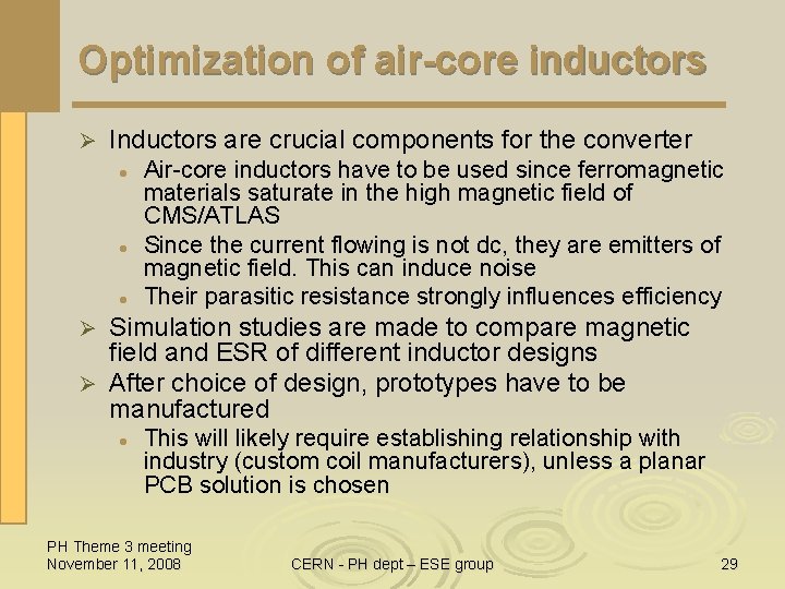
Optimization of air-core inductors Ø Inductors are crucial components for the converter l l l Air-core inductors have to be used since ferromagnetic materials saturate in the high magnetic field of CMS/ATLAS Since the current flowing is not dc, they are emitters of magnetic field. This can induce noise Their parasitic resistance strongly influences efficiency Simulation studies are made to compare magnetic field and ESR of different inductor designs Ø After choice of design, prototypes have to be manufactured Ø l This will likely require establishing relationship with industry (custom coil manufacturers), unless a planar PCB solution is chosen PH Theme 3 meeting November 11, 2008 CERN - PH dept – ESE group 29

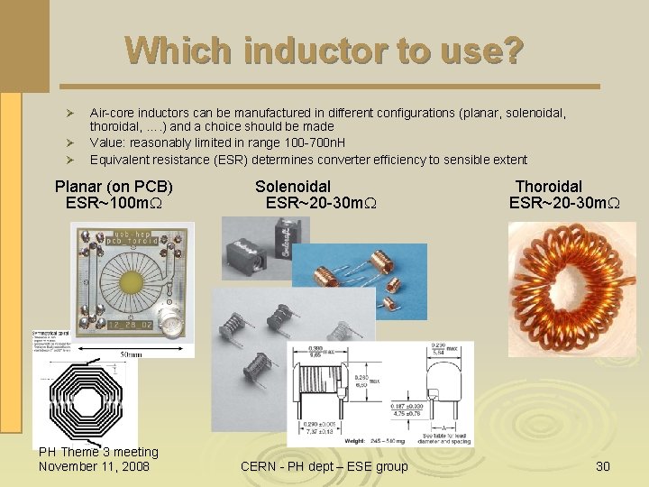
Which inductor to use? Ø Ø Ø Air-core inductors can be manufactured in different configurations (planar, solenoidal, thoroidal, …. ) and a choice should be made Value: reasonably limited in range 100 -700 n. H Equivalent resistance (ESR) determines converter efficiency to sensible extent Planar (on PCB) ESR~100 m. W PH Theme 3 meeting November 11, 2008 Solenoidal ESR~20 -30 m. W CERN - PH dept – ESE group Thoroidal ESR~20 -30 m. W 30

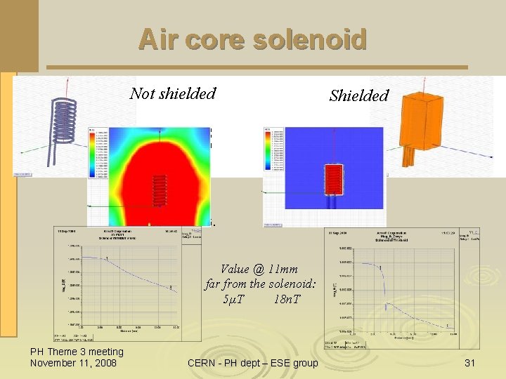
Air core solenoid Not shielded Shielded Value @ 11 mm far from the solenoid: 5µT 18 n. T PH Theme 3 meeting November 11, 2008 CERN - PH dept – ESE group 31

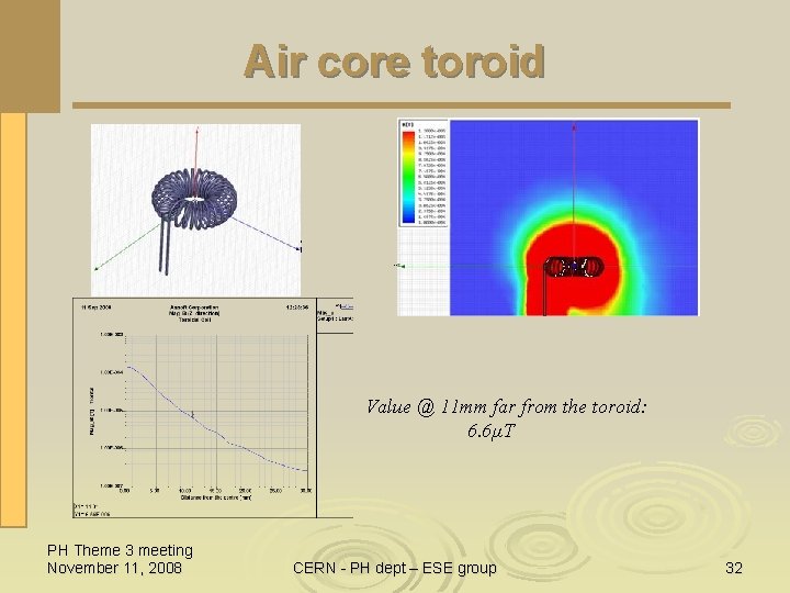
Air core toroid Value @ 11 mm far from the toroid: 6. 6µT PH Theme 3 meeting November 11, 2008 CERN - PH dept – ESE group 32

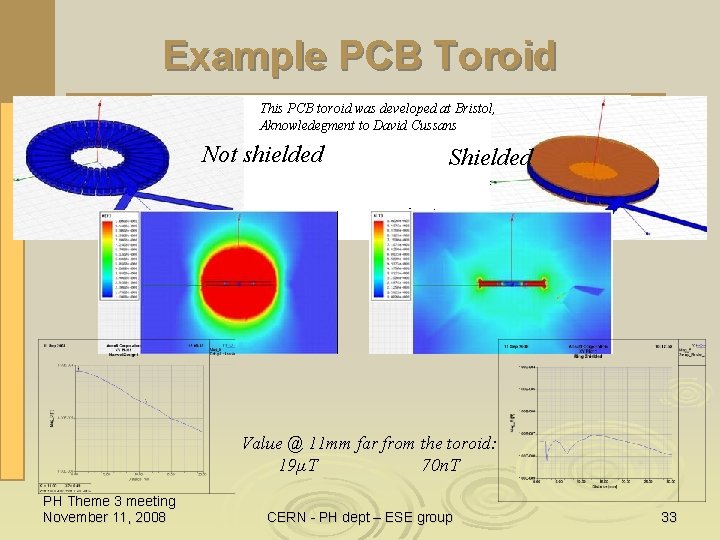
Example PCB Toroid This PCB toroid was developed at Bristol, Aknowledegment to David Cussans Not shielded Shielded Value @ 11 mm far from the toroid: 19µT 70 n. T PH Theme 3 meeting November 11, 2008 CERN - PH dept – ESE group 33

WP 2 -2 and 2 -3: deliverables Ø WP 2 -2 Deliverables (in parenthesis also WP 2 -3) : Evaluation report on conversion technologies, (including consultancy report) Report 31 -Mar-09 Prototypes of converters (and inductors) with viability report, (CMOS qualification report) Prototype, Report 31 -Mar-10 Integration in full-scale detector modules Demonstrator 31 -Mar-11 Ø Specific Additions in WP 2 -3 l Consultancy to procure expertise in power electronics l Transformer based on piezoelectric ceramic materials l Second source CMOS technology l Optimization of air-core inductor PH Theme 3 meeting November 11, 2008 CERN - PH dept – ESE group 34

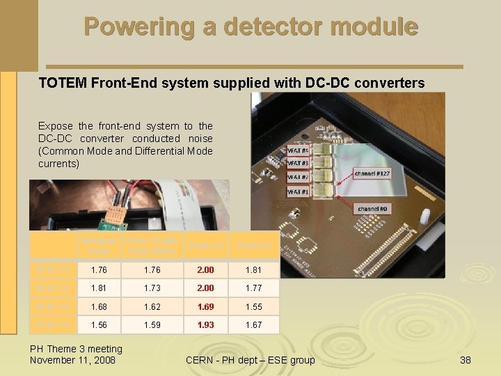
Integration in detector modules Ø Main issues for integration: EMC and physical space Ø EMC l l Measurements of noise (conducted and radiated) on converter prototypes Module-level tests • @ RWTH Aachen with CMS TEC modules • @ CERN with TOTEM Si Strip modules PH Theme 3 meeting November 11, 2008 CERN - PH dept – ESE group 35

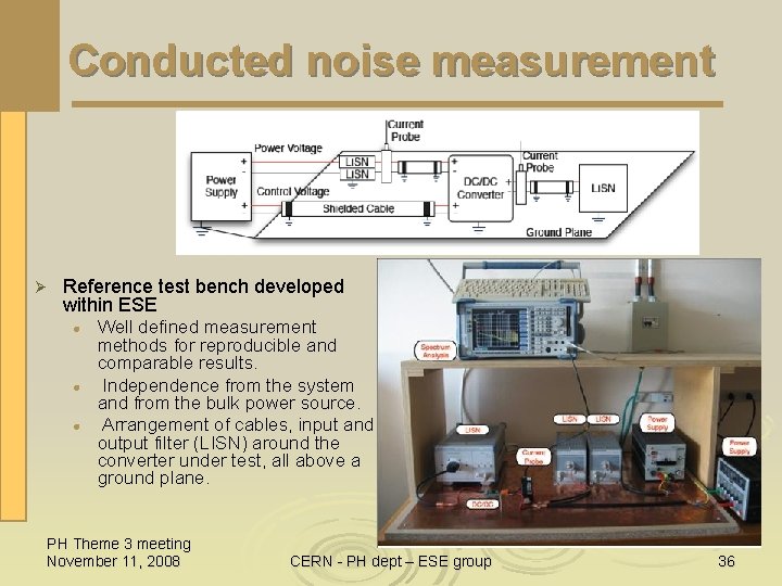
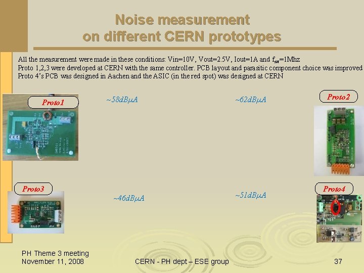
Conducted noise measurement Ø Reference test bench developed within ESE l l l Well defined measurement methods for reproducible and comparable results. Independence from the system and from the bulk power source. Arrangement of cables, input and output filter (LISN) around the converter under test, all above a ground plane. PH Theme 3 meeting November 11, 2008 CERN - PH dept – ESE group 36

Noise measurement on different CERN prototypes All the measurement were made in these conditions: Vin=10 V, Vout=2. 5 V, Iout=1 A and fsw=1 Mhz Proto 1, 2, 3 were developed at CERN with the same controller. PCB layout and parasitic component choice was improved Proto 4’s PCB was designed in Aachen and the ASIC (in the red spot) was designed at CERN Proto 1 ~58 d. BµA Proto 3 ~46 d. BµA PH Theme 3 meeting November 11, 2008 CERN - PH dept – ESE group ~62 d. BµA ~51 d. BµA Proto 2 Proto 4 37

Powering a detector module TOTEM Front-End system supplied with DC-DC converters Expose the front-end system to the DC-DC converter conducted noise (Common Mode and Differential Mode currents) Nominal noise Proto #3 with long cables Proto #3 Proto #4 VFAT #1 1. 76 2. 00 1. 81 VFAT #2 1. 81 1. 73 2. 00 1. 77 VFAT #3 1. 68 1. 62 1. 69 1. 55 VFAT #4 1. 56 1. 59 1. 93 1. 67 PH Theme 3 meeting November 11, 2008 CERN - PH dept – ESE group 38

WP 2 -2 and 2 -3: deliverables Ø WP 2 -2 Deliverables (in parenthesis also WP 2 -3) : Evaluation report on conversion technologies, (including consultancy report) Report 31 -Mar-09 Prototypes of converters (and inductors) with viability report, (CMOS qualification report) Prototype, Report 31 -Mar-10 Integration in full-scale detector modules Demonstrator 31 -Mar-11 Ø Specific Additions in WP 2 -3 l Consultancy to procure expertise in power electronics l Transformer based on piezoelectric ceramic materials l Second source CMOS technology l Optimization of air-core inductor PH Theme 3 meeting November 11, 2008 CERN - PH dept – ESE group 39

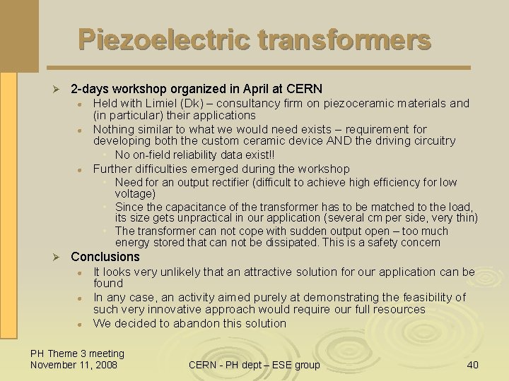
Piezoelectric transformers Ø 2 -days workshop organized in April at CERN l l l Held with Limiel (Dk) – consultancy firm on piezoceramic materials and (in particular) their applications Nothing similar to what we would need exists – requirement for developing both the custom ceramic device AND the driving circuitry • No on-field reliability data exist!! Further difficulties emerged during the workshop • Need for an output rectifier (difficult to achieve high efficiency for low voltage) • Since the capacitance of the transformer has to be matched to the load, its size gets unpractical in our application (several cm per side, very thin) • The transformer can not cope with sudden output open – too much energy stored that can not be dissipated. This is a safety concern Ø Conclusions l l l It looks very unlikely that an attractive solution for our application can be found In any case, an activity aimed purely at demonstrating the feasibility of such very innovative approach would require our full resources We decided to abandon this solution PH Theme 3 meeting November 11, 2008 CERN - PH dept – ESE group 40

Outline Introduction Ø Project structure Ø l l l Ø Working Team Communication Composition of WP 2 Technical status l l WP 2 -1 WP 2 -2 and 2 -3 Resources Ø Conclusion Ø PH Theme 3 meeting November 11, 2008 CERN - PH dept – ESE group 41

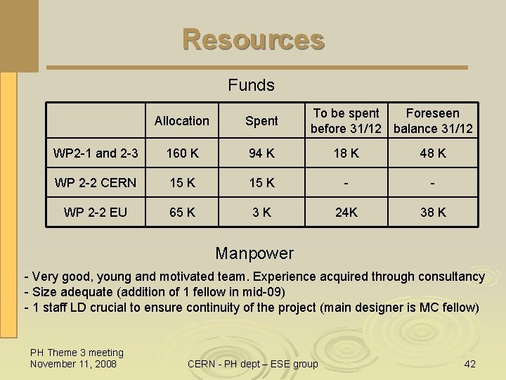
Resources Funds To be spent Foreseen before 31/12 balance 31/12 Allocation Spent WP 2 -1 and 2 -3 160 K 94 K 18 K 48 K WP 2 -2 CERN 15 K - - WP 2 -2 EU 65 K 3 K 24 K 38 K Manpower - Very good, young and motivated team. Experience acquired through consultancy - Size adequate (addition of 1 fellow in mid-09) - 1 staff LD crucial to ensure continuity of the project (main designer is MC fellow) PH Theme 3 meeting November 11, 2008 CERN - PH dept – ESE group 42

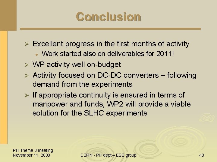
Conclusion Ø Excellent progress in the first months of activity l Work started also on deliverables for 2011! WP activity well on-budget Ø Activity focused on DC-DC converters – following demand from the experiments Ø If appropriate continuity is ensured in terms of manpower and funds, WP 2 will provide a viable solution for the SLHC experiments Ø PH Theme 3 meeting November 11, 2008 CERN - PH dept – ESE group 43