Woodpile Structure Fabrication Chris Mc Guinness July 8

Woodpile Structure Fabrication Chris Mc. Guinness July 8, 2009 Workshop on Novel Concepts for Linear Accelerators and Colliders Working Group 2: Dielectric Laser Accelerators

Outline • • • Motivation Fabrication Process Fabrication Parameters Layer Adhesion Future Plans
 Si.")
Motivations Sources Gradient 101 Zn. S Eacc=1. 04 GV/m @5μm(6 e 4 GHZ) Si. O 2 Eacc=2. 76 GV/m @800 nm(3. 75 e 5 GHZ) Al 3 O 2 Eacc=2. 0 GV/m @800 nm(3. 75 e 5 GHZ) 0 Si Eacc=337 MV/m @1550 nm(1. 94 e 5 GHZ) Ratio=1. 41 Fabrication

Fabrication Process Si. O 2 Photo resist 2 Si. O 2 1 Si Substrate h Step 1: Si. O 2 Deposition - LPCVD • Uniformity = 1 -2% • Controllability = 7% resist Silicon Substrate Step 2: Resist Coat a w 3 4 Step 3: Optical Lithography • Minimum feature size 450 nm • Alignment 3σ=60 nm Poly-si Step 4: Plasma etch Si. O 2 poly-si 5 Step 5: Poly-si Deposition Silicon Substrate

6 Step 6: Chemical Mechanical Polish Frictional Force Fabrication Process 10 sec=15 nm Time Si. O 2 7 Step 7: Repeat process for remaining layers 8 Final Step: HF Vapor Etch poly-si

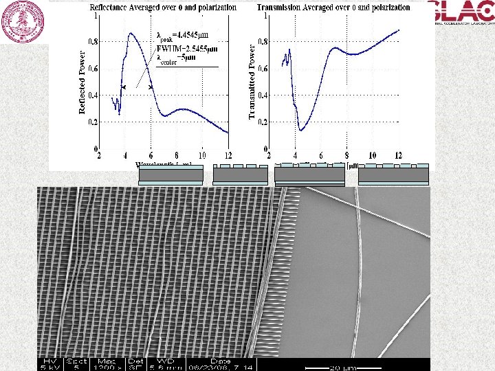
Four Layer Test Structure

Fabrication Deviations Parameter Summary Target Measured Rod Width 500 nm 498 nm ± 74 nm Tapper Angle 0 o 10. 4 o ± 0. 6 o Layer Thickness 632 nm 611 nm ± 73 nm Alignment Offset <80 nm 138 nm

Tapper Angle AMT 8100 - Hexode Plasma Etcher CHF 3 85 sccm O 2 6 sccm CHF 3 50 sccm O 2 30 sccm 5. 1 o 6. 6 o P 5000 -Magnetically Enhanced RIE CF 4 50 sccm CH 3 F 20 sccm Ar 100 sccm CF 4 50 sccm CH 3 F 25 sccm Ar 120 sccm 3. 4 o ~0 o

Rod Width Measurement Resolution ~25 nm

Layer Thickness Deposition – LPCVD TEOS • Uniformity = 1 -2% • Controllability = 7%

Layer Adhesion

Stress

Annealed Wafer HF Vapor Etch Not Annealed, Buffered HF Etch Not Annealed, Vapor HF Etched Annealed, Buffered HF Etch Annealed, Vapor HF Etch

Measure Adhesion Strength . . .

Future Direction • Complete 15 layer structure • Optical measurements – Spectroscopy – Coupling – Mode excitation • Beam measurements – Wakefield modes • Simulations – Consider fabrication variations – Couplers

THE END

FTIR Spectroscopy Measurements
")
Finite Thickness Simulation Reflection/Transmission (averaged over S&P polarizations, and polar angle θ, φ=0)
")
Simulation Reflection/Transmission (averaged over S&P polarizations, and polar angle θ, φ=0)

Simulation vs. Measurement Bandgap from MPB
- Slides: 21