
Wire Scanner AFE Electronics results from WS AFE

- Slides: 31
Wire Scanner AFE Electronics: results from WS AFE tests at CERN LINAC 4 ESS 4 th BI Forum Raffaele De Monte, Nov 21, 2017 2
ESS WS tests @ CERN LINAC 4 Test phases September 2017 @ elettra: • Test feasibility study • Test diagram definition • Preparation of cable adapters 10 -11 Oct 2017 during LINAC 4 shutdown: (M. Ferianis, S. Cleva, R. De Monte) • Installation of AFE in LINAC 4 tunnel • Temporary installation of all acquisition electronics in LINAC 4 Service area • Preliminary test without beam of ALL the electronics • Removing the temporary installation of all acquisition electronics 8 -9 November 2017 during LINAC 4 operations: (M. Ferianis, S. Cleva, R. De Monte) • Reinstall of all acquisition electronics in LINAC 4 Service area for test • Tests the electronics with a real beam! • Remove ALL the electronics (including AFE from tunnel) ESS 4 th BI Forum Raffaele De Monte, Nov 21, 2017
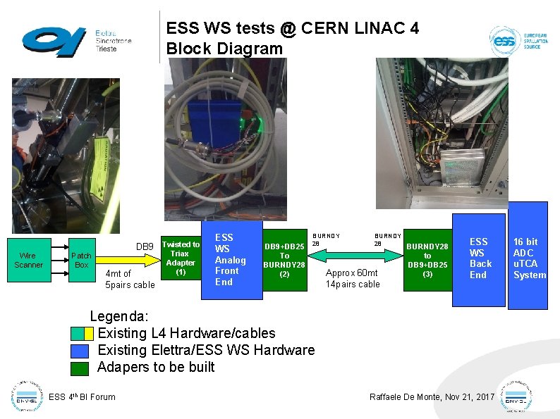
ESS WS tests @ CERN LINAC 4 Block Diagram Wire Scanner Patch Box DB 9 4 mt of 5 pairs cable Twisted to Triax Adapter (1) ESS WS Analog Front End DB 9+DB 25 To BURNDY 28 (2) BURNDY 28 Approx 60 mt 14 pairs cable BURNDY 28 to DB 9+DB 25 (3) ESS WS Back End Legenda: Existing L 4 Hardware/cables Existing Elettra/ESS WS Hardware Adapers to be built ESS 4 th BI Forum Raffaele De Monte, Nov 21, 2017 16 bit ADC u. TCA System
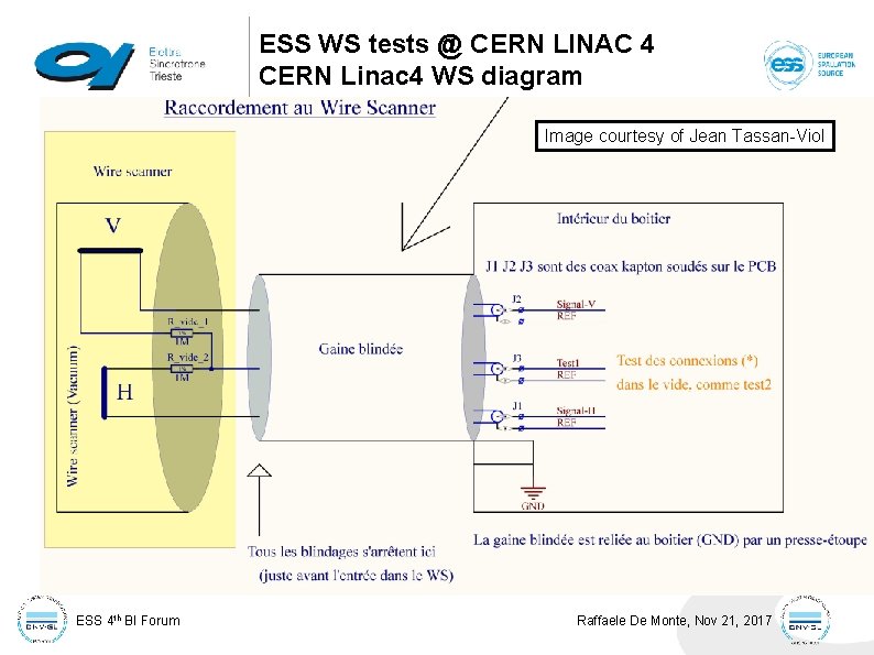
ESS WS tests @ CERN LINAC 4 CERN Linac 4 WS diagram Image courtesy of Jean Tassan-Viol ESS 4 th BI Forum Raffaele De Monte, Nov 21, 2017
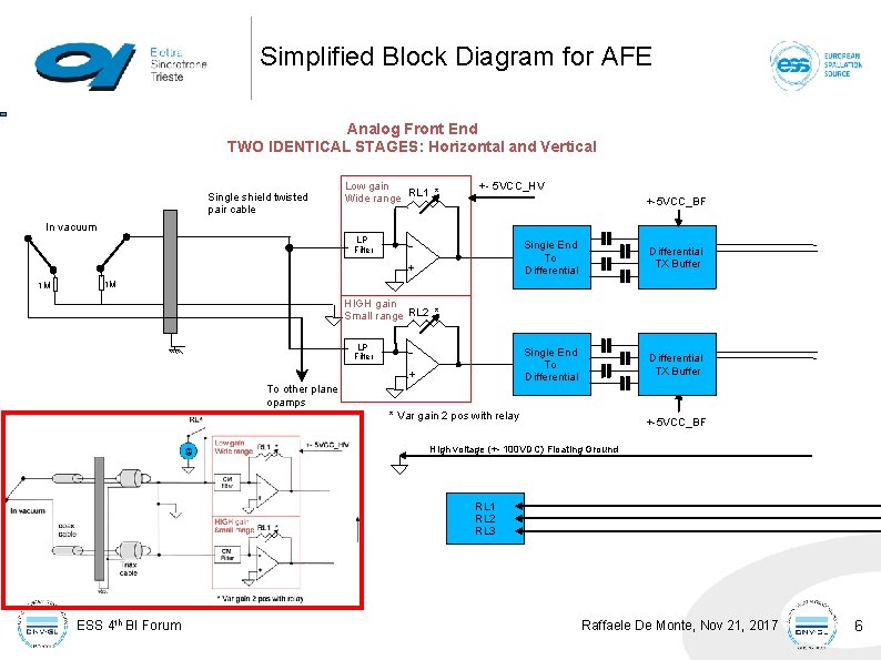
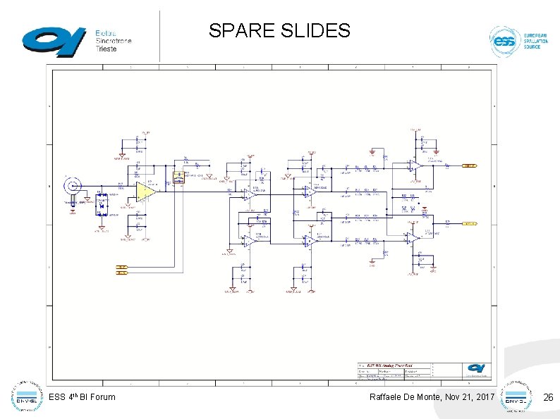
Simplified Block Diagram for AFE Analog Front End TWO IDENTICAL STAGES: Horizontal and Vertical Single shield twisted pair cable Low gain RL 1 * Wide range +- 5 VCC_HV +-5 VCC_BF In vacuum LP Filter + 1 M Single End To Differential TX Buffer 1 M HIGH gain Small range RL 2 * LP Filter + To other plane opamps * Var gain 2 pos with relay +-5 VCC_BF High voltage (+- 100 VDC) Floating Ground RL 1 RL 2 RL 3 ESS 4 th BI Forum Raffaele De Monte, Nov 21, 2017 6
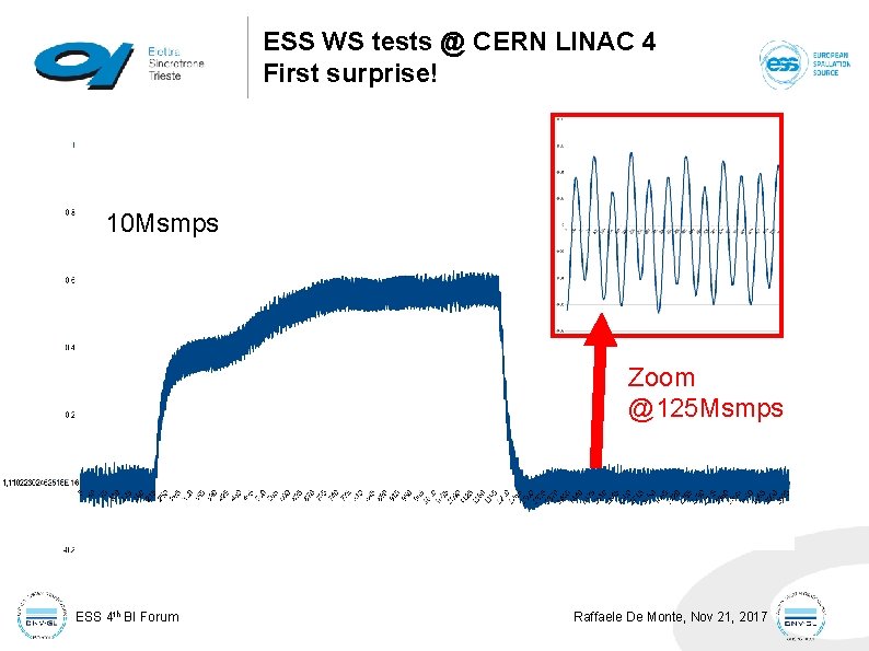
ESS WS tests @ CERN LINAC 4 First surprise! 10 Msmps Zoom @125 Msmps ESS 4 th BI Forum Raffaele De Monte, Nov 21, 2017
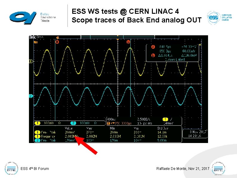
ESS WS tests @ CERN LINAC 4 Scope traces of Back End analog OUT ESS 4 th BI Forum Raffaele De Monte, Nov 21, 2017
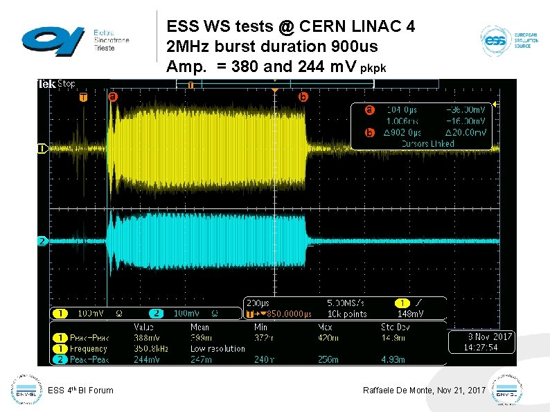
ESS WS tests @ CERN LINAC 4 2 MHz burst duration 900 us Amp. = 380 and 244 m. V pkpk ESS 4 th BI Forum Raffaele De Monte, Nov 21, 2017
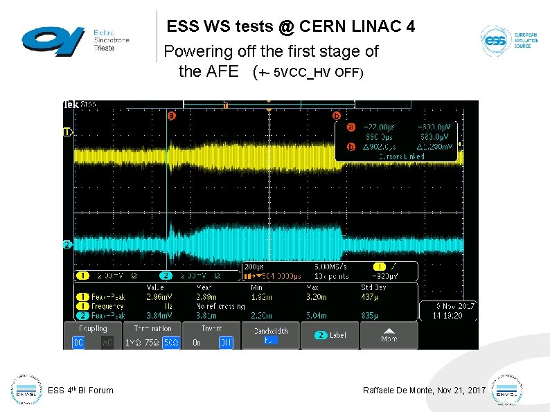
ESS WS tests @ CERN LINAC 4 Powering off the first stage of the AFE (+- 5 VCC_HV OFF) ESS 4 th BI Forum Raffaele De Monte, Nov 21, 2017
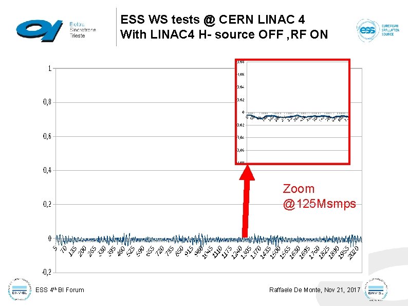
ESS WS tests @ CERN LINAC 4 With LINAC 4 H- source OFF , RF ON Zoom @125 Msmps ESS 4 th BI Forum Raffaele De Monte, Nov 21, 2017
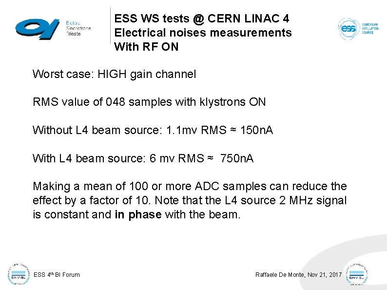
ESS WS tests @ CERN LINAC 4 Electrical noises measurements With RF ON Worst case: HIGH gain channel RMS value of 048 samples with klystrons ON Without L 4 beam source: 1. 1 mv RMS ≈ 150 n. A With L 4 beam source: 6 mv RMS ≈ 750 n. A Making a mean of 100 or more ADC samples can reduce the effect by a factor of 10. Note that the L 4 source 2 MHz signal is constant and in phase with the beam. ESS 4 th BI Forum Raffaele De Monte, Nov 21, 2017
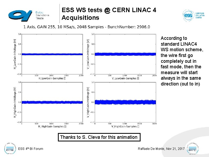
ESS WS tests @ CERN LINAC 4 Acquisitions According to standard LINAC 4 WS motion scheme, the wire first go completely out in fast mode, then the measure will start always in the same direction (out to in) Thanks to S. Cleva for this animation ESS 4 th BI Forum Raffaele De Monte, Nov 21, 2017
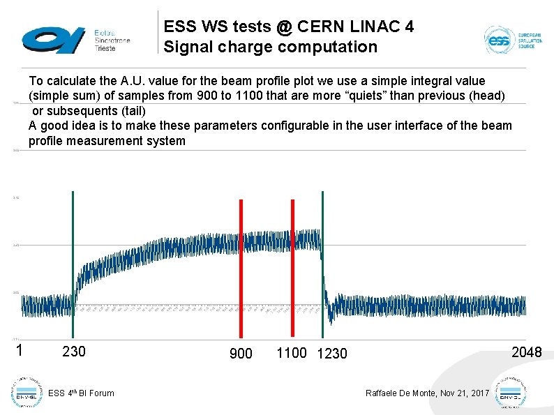
ESS WS tests @ CERN LINAC 4 Signal charge computation To calculate the A. U. value for the beam profile plot we use a simple integral value (simple sum) of samples from 900 to 1100 that are more “quiets” than previous (head) or subsequents (tail) A good idea is to make these parameters configurable in the user interface of the beam profile measurement system 1 230 ESS 4 th BI Forum 900 2048 1100 1230 Raffaele De Monte, Nov 21, 2017
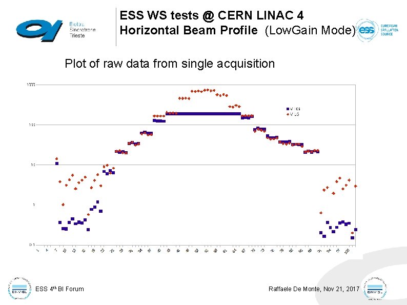
ESS WS tests @ CERN LINAC 4 Horizontal Beam Profile (Low. Gain Mode) Plot of raw data from single acquisition ESS 4 th BI Forum Raffaele De Monte, Nov 21, 2017
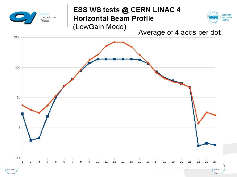
ESS WS tests @ CERN LINAC 4 Horizontal Beam Profile (Low. Gain Mode) Average of 4 acqs per dot ESS 4 th BI Forum Raffaele De Monte, Nov 21, 2017
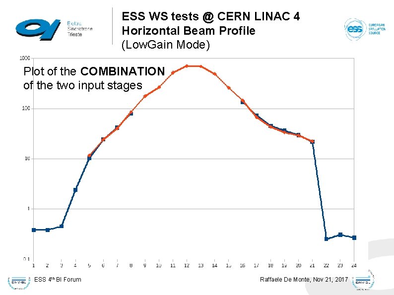
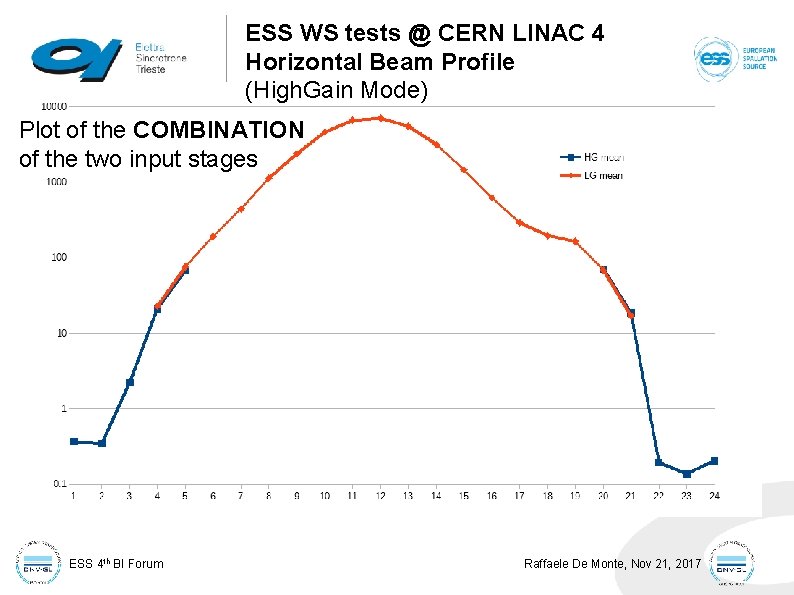
ESS WS tests @ CERN LINAC 4 Horizontal Beam Profile (Low. Gain Mode) Plot of the COMBINATION of the two input stages ESS 4 th BI Forum Raffaele De Monte, Nov 21, 2017
ESS WS tests @ CERN LINAC 4 Horizontal Beam Profile (High. Gain Mode) Plot of the COMBINATION of the two input stages ESS 4 th BI Forum Raffaele De Monte, Nov 21, 2017
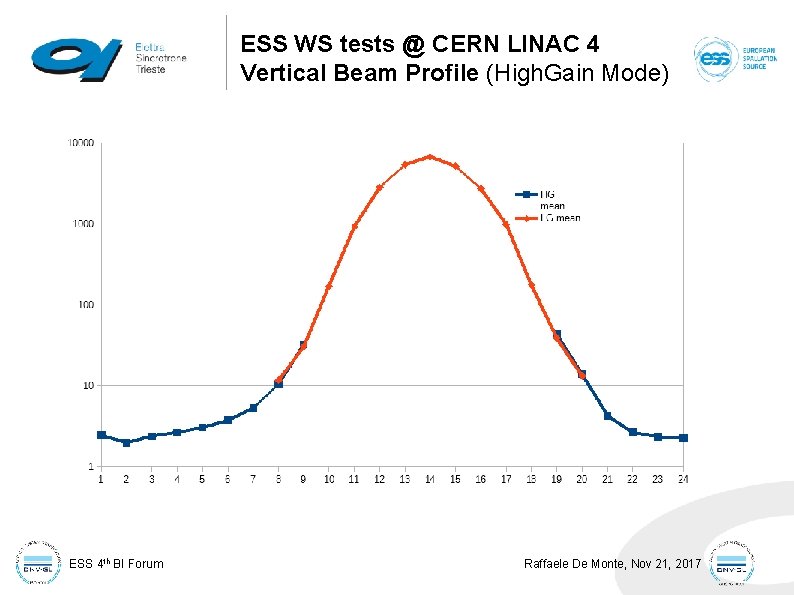
ESS WS tests @ CERN LINAC 4 Vertical Beam Profile (High. Gain Mode) ESS 4 th BI Forum Raffaele De Monte, Nov 21, 2017
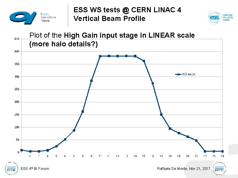
ESS WS tests @ CERN LINAC 4 Vertical Beam Profile Plot of the High Gain input stage in LINEAR scale (more halo details? ) ESS 4 th BI Forum Raffaele De Monte, Nov 21, 2017
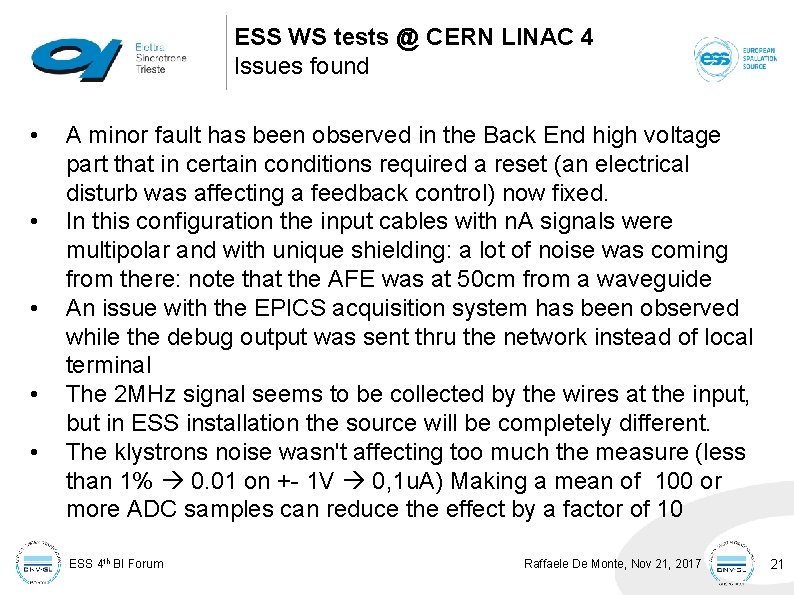
ESS WS tests @ CERN LINAC 4 Issues found • • • A minor fault has been observed in the Back End high voltage part that in certain conditions required a reset (an electrical disturb was affecting a feedback control) now fixed. In this configuration the input cables with n. A signals were multipolar and with unique shielding: a lot of noise was coming from there: note that the AFE was at 50 cm from a waveguide An issue with the EPICS acquisition system has been observed while the debug output was sent thru the network instead of local terminal The 2 MHz signal seems to be collected by the wires at the input, but in ESS installation the source will be completely different. The klystrons noise wasn't affecting too much the measure (less than 1% 0. 01 on +- 1 V 0, 1 u. A) Making a mean of 100 or more ADC samples can reduce the effect by a factor of 10 ESS 4 th BI Forum Raffaele De Monte, Nov 21, 2017 21
ESS WS tests @ CERN LINAC 4 Considerations /Conclusions • • • The working principle of the extended range analog front end has been tested with a real beam and it works as expected The signal cables and all the current detection part should be shielded as much as possible The 2 MHz signal coming from L 4 source is affecting our measure, but also with this big issue we measure with a 4 decades range Without this disturb, at least a factor of 5 will get back A laboratory calibration is possible using the in house developed “wire scanner electronic simulator” because we tested that is very similar to the real beam An automated calibration procedure, using a programmable pulse generator and our “wire scanner electronic simulator” will be performed to create an exhaustive calibration table that will be used by the software to use as best as possible the combination of the two amplifiers (LO and HI gain) ESS 4 th BI Forum Raffaele De Monte, Nov 21, 2017 22
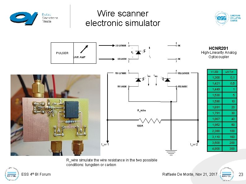
Wire scanner electronic simulator HCNR 201 High-Linearity Analog Optocoupler PULSER VAR AMP V LED R_wire 100 R I_w 1 I_w 2 u. A Tot 1, 300 0, 1 1, 421 0, 5 1, 449 1 1, 530 5 1, 590 10 1, 691 20 1, 791 30 1, 867 40 1, 952 50 2, 380 100 3, 110 160 3, 500 200 4, 800 300 R_wire simulate the wire resistance in the two possibile conditions: tungsten or carbon ESS 4 th BI Forum Raffaele De Monte, Nov 21, 2017 23
Acknowledgments In these two trips at CERN's LINAC 4 we were able to learn a lot of useful information about the PRACTICAL operation of beam profile measurement in a real proton LINAC environment with Wire Scanner. Many Thanks to: • • Federico Roncarolo Jean Tassan-Viol all of the LINAC 4 Beam diagnostics staff and the LINAC 4 operators Thank you for your attention ESS 4 th BI Forum Raffaele De Monte, Nov 21, 2017
SPARE SLIDES ESS 4 th BI Forum Raffaele De Monte, Nov 21, 2017 26
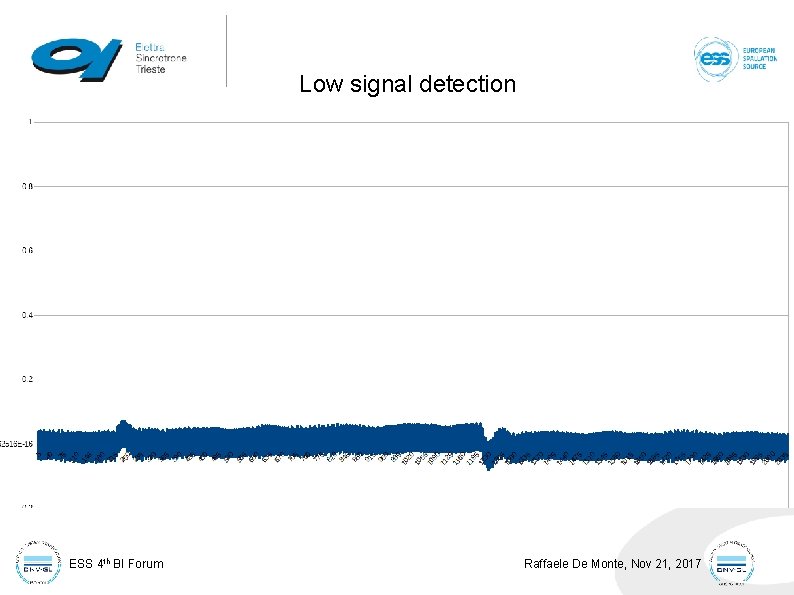
Low signal detection ESS 4 th BI Forum Raffaele De Monte, Nov 21, 2017
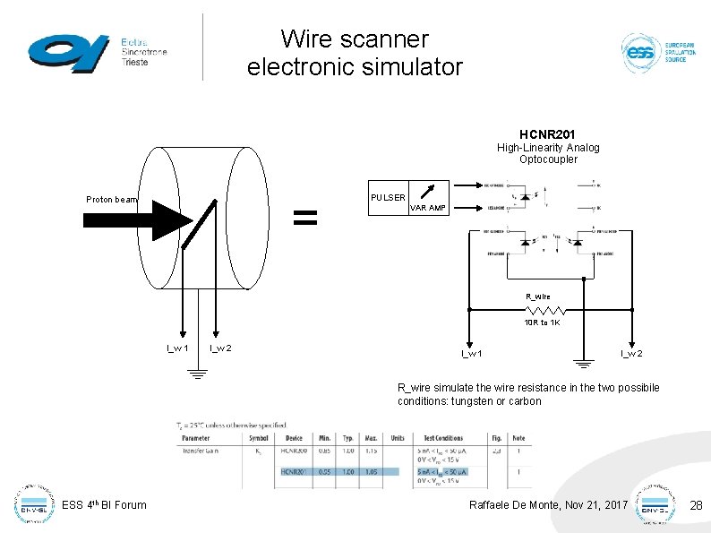
Wire scanner electronic simulator HCNR 201 High-Linearity Analog Optocoupler = Proton beam PULSER VAR AMP R_wire 10 R to 1 K I_w 1 I_w 2 R_wire simulate the wire resistance in the two possibile conditions: tungsten or carbon ESS 4 th BI Forum Raffaele De Monte, Nov 21, 2017 28
SPARE SLIDES ESS 4 th BI Forum Raffaele De Monte, Nov 21, 2017
Analog Opto Current Pulse Generator Signal simulation: It is necessary to generate two pulsed signals, equals and with ultra low currents to feed the AFE prototype. Square Wave Pulses: from 10 n. A to 400µA , from 10µs to 100µs. Commercial available current generators aren’t able to simulate this kind of signals. We are using an in-house developed solution. The beam's simulator is made using an analog high precision optocoupler driven by a pulser with variabile output. The circuit is calibrated in DC, by driving the variable current/voltage circuit and reading the output with pico-ammeter. Then the known current/voltage driving will be pulsed. To validate this method we also put a DC current from Keythley pico. Ampere source generator at the circuit input and we measure the corresponding voltage from TIA (Transimpedance Input Amplifier) at various currents from 100 n. A to 300µA. ESS 4 th BI Forum Raffaele De Monte, Nov 21, 2017 30
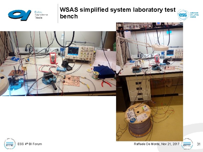
WSAS simplified system laboratory test bench ESS 4 th BI Forum Raffaele De Monte, Nov 21, 2017 31