Whats a modulated structure Mutidimensional direct methods of




![Electron diffraction analysis of the Bi-2223 superconductor Space group: P [Bbmb] 1 -1 1 Electron diffraction analysis of the Bi-2223 superconductor Space group: P [Bbmb] 1 -1 1](https://slidetodoc.com/presentation_image_h2/a6b554d7deebc0ca457f895750e0f0c3/image-13.jpg)
![Bi-2223 [100] projected potential Space group: P [Bbmb] 1 -1 1 a = 5. Bi-2223 [100] projected potential Space group: P [Bbmb] 1 -1 1 a = 5.](https://slidetodoc.com/presentation_image_h2/a6b554d7deebc0ca457f895750e0f0c3/image-14.jpg)
![Image Processing of Bi-2212 EM image from Dr. S. Horiuchi Space group: N [Bbmb] Image Processing of Bi-2212 EM image from Dr. S. Horiuchi Space group: N [Bbmb]](https://slidetodoc.com/presentation_image_h2/a6b554d7deebc0ca457f895750e0f0c3/image-16.jpg)
![Electron diffraction analysis of Bi-2201 Space group: P[B 2/b] -1]; a = 5. 41, Electron diffraction analysis of Bi-2201 Space group: P[B 2/b] -1]; a = 5. 41,](https://slidetodoc.com/presentation_image_h2/a6b554d7deebc0ca457f895750e0f0c3/image-18.jpg)
- Slides: 20

What’s a modulated structure ? Muti-dimensional direct methods of solving modulated structures Incommesurate modulation in Bi-based supercondutors from electron crystallography

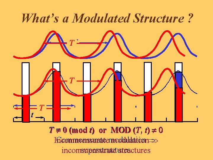
What’s a Modulated Structure ? TT T t T T T= ¹ 0 (mod t) or MOD (T, t) = ¹ 0 Commensurate modulation Incommensurate modulationÞ Þ superstructures incommensurate structures

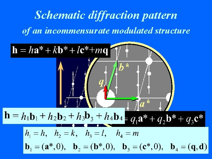
Schematic diffraction pattern of an incommensurate modulated structure b* q a*

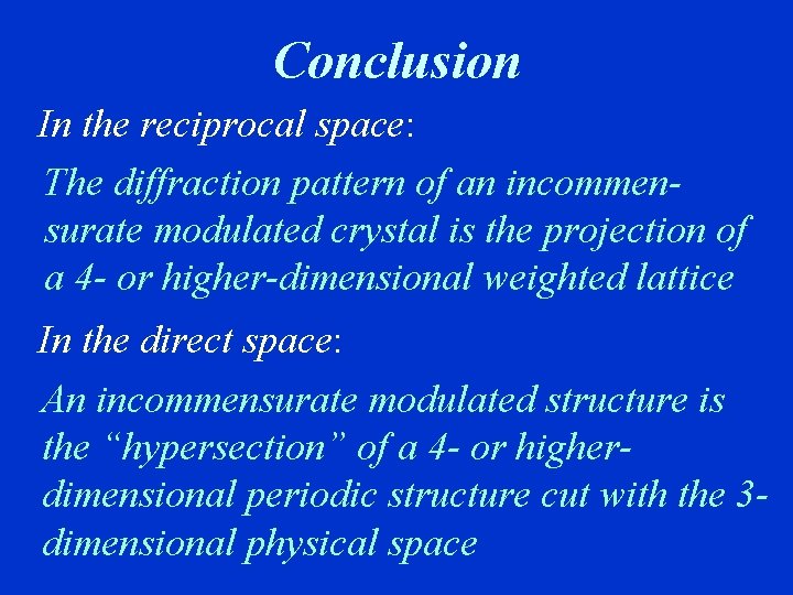
Conclusion In the reciprocal space: The diffraction pattern of an incommensurate modulated crystal is the projection of a 4 - or higher-dimensional weighted lattice In the direct space: An incommensurate modulated structure is the “hypersection” of a 4 - or higherdimensional periodic structure cut with the 3 dimensional physical space

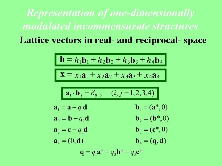
Representation of one-dimensionally modulated incommensurate structures Lattice vectors in real- and reciprocal- space

Structure-factor formula Modulated atoms situated at their average positions

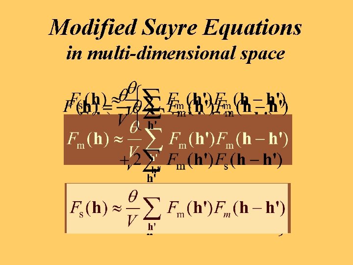
Modified Sayre Equations in multi-dimensional space

Strategy of solving incommensurate modulated structures i) Derive phases of main reflections using ii) Derive phases of satellite reflections using iii) Calculate the multi-dimensional Fourier map iv) Cut the resulting Fourier map with the 3 -D ‘hyperplane’ (3 -D physical space) v) Parameters of the modulation functions are measured directly on the multi-dimensional Fourier map

Electron Crystallographic Study of Bi-based Superconductors using Multi-dimensional Direct Methods

Why Electrons ? 1. Electrons are better for studying minute and imperfect crystalline samples 2. Electron microscopes are the only instrument that can produce simultaneously EM’s and ED’s for the same crystalline sample at atomic resolution 3. Electrons are better for revealing light atoms in the presence of heavy atoms

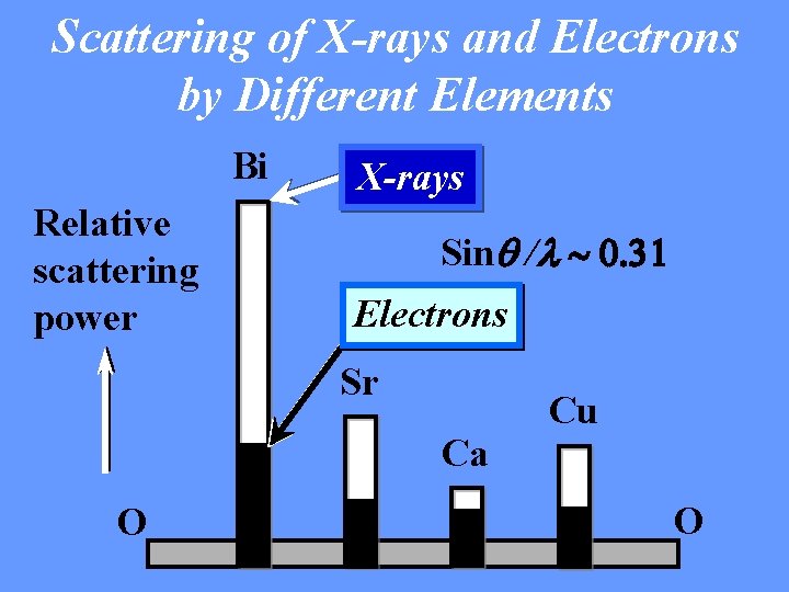
Scattering of X-rays and Electrons by Different Elements Bi Relative scattering power X-rays Sinq /l ~ 0. 31 Electrons Sr Ca O Cu O

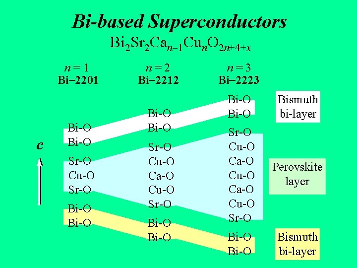
Bi-based Superconductors Bi 2 Sr 2 Can-1 Cun. O 2 n+4+x n=1 Bi-2201 c Bi-O Sr-O Cu-O Sr-O Bi-O n=2 Bi-2212 Bi-O Sr-O Cu-O Ca-O Cu-O Sr-O Bi-O n=3 Bi-2223 Bi-O Bismuth bi-layer Sr-O Cu-O Ca-O Cu-O Sr-O Perovskite layer Bi-O Bismuth bi-layer
![Electron diffraction analysis of the Bi2223 superconductor Space group P Bbmb 1 1 1 Electron diffraction analysis of the Bi-2223 superconductor Space group: P [Bbmb] 1 -1 1](https://slidetodoc.com/presentation_image_h2/a6b554d7deebc0ca457f895750e0f0c3/image-13.jpg)
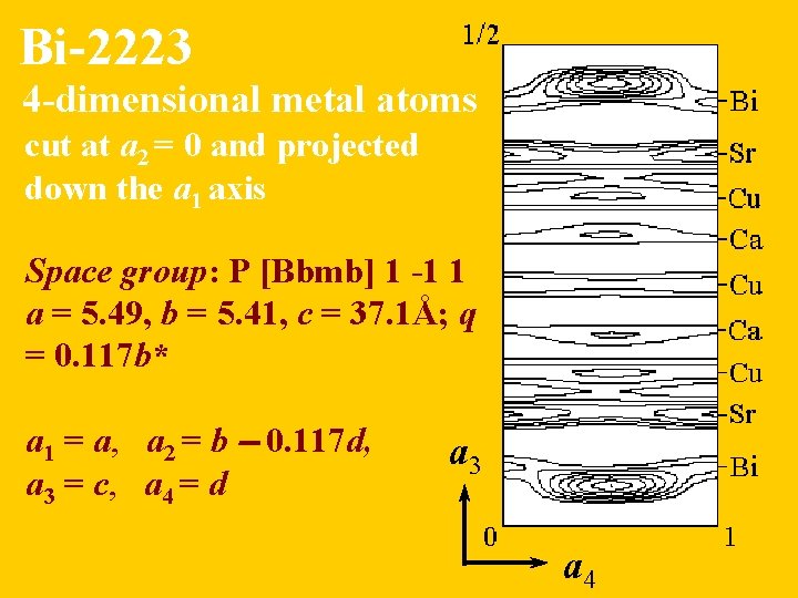
Electron diffraction analysis of the Bi-2223 superconductor Space group: P [Bbmb] 1 -1 1 a = 5. 49, b = 5. 41, c = 37. 1Å; q = 0. 117 b* *The average structure is known*
![Bi2223 100 projected potential Space group P Bbmb 1 1 1 a 5 Bi-2223 [100] projected potential Space group: P [Bbmb] 1 -1 1 a = 5.](https://slidetodoc.com/presentation_image_h2/a6b554d7deebc0ca457f895750e0f0c3/image-14.jpg)
Bi-2223 [100] projected potential Space group: P [Bbmb] 1 -1 1 a = 5. 49, b = 5. 41, c = 37. 1Å; q = 0. 117 b* Rsym. M = 0. 12 (Nref. =42) Rsym. S = 0. 13 (Nref. = 70) Rm = 0. 16 Rs = 0. 17

Bi-2223 4 -dimensional metal atoms cut at a 2 = 0 and projected down the a 1 axis Space group: P [Bbmb] 1 -1 1 a = 5. 49, b = 5. 41, c = 37. 1Å; q = 0. 117 b* a 1 = a, a 2 = b - 0. 117 d, a 3 = c, a 4 = d a 3 a 4
![Image Processing of Bi2212 EM image from Dr S Horiuchi Space group N Bbmb Image Processing of Bi-2212 EM image from Dr. S. Horiuchi Space group: N [Bbmb]](https://slidetodoc.com/presentation_image_h2/a6b554d7deebc0ca457f895750e0f0c3/image-16.jpg)
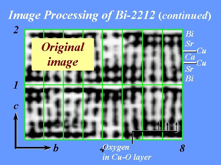
Image Processing of Bi-2212 EM image from Dr. S. Horiuchi Space group: N [Bbmb] 1 -1 1 a = 5. 42, b = 5. 44, c = 30. 5Å; q = 0. 22 b* + c* FT Phase -1 extension FT

Image Processing of Bi-2212 (continued) 2 Bi Sr Original Enhanced image Cu Ca Cu Sr Bi 1 c b 4 Oxygen in Cu-O layer 8
![Electron diffraction analysis of Bi2201 Space group PB 2b 1 a 5 41 Electron diffraction analysis of Bi-2201 Space group: P[B 2/b] -1]; a = 5. 41,](https://slidetodoc.com/presentation_image_h2/a6b554d7deebc0ca457f895750e0f0c3/image-18.jpg)
Electron diffraction analysis of Bi-2201 Space group: P[B 2/b] -1]; a = 5. 41, b = 5. 43, c = 24. 6Å, b = 90 o; q = 0. 217 b* + 0. 62 c* O atoms on the Cu-O layer c b O (extra) Bi-O Sr-O Cu-O Sr-O Bi-O RT = 0. 32 Rm = 0. 29 RS 1 = 0. 29 RS 2 = 0. 36 RS 3 = 0. 52

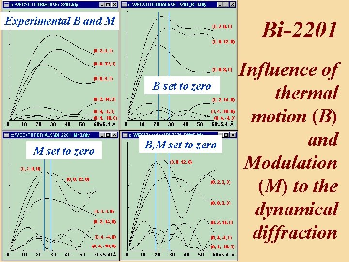
Experimental B and M Bi-2201 B set to zero M set to zero B, M set to zero Influence of thermal motion (B) and Modulation (M) to the dynamical diffraction

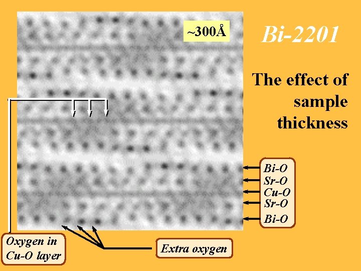
Sample thickness: ~300Å ~100Å ~200Å ~5Å Bi-2201 The effect of sample thickness Bi-O Sr-O Cu-O Sr-O Bi-O Oxygen in Cu-O layer Extra oxygen