
What GPGPUSim Simulates 1 Functional model for PTXSASS

- Slides: 61
What GPGPU-Sim Simulates 1. Functional model for PTX/SASS – PTX = Parallel Thread e. Xecution • A scalar low-level, data-parallel virtual ISA defined by Nvidia – SASS = Native ISA for Nvidia GPUs – Not Direct. X, Not shader model N, Not AMD’s ISA, Not x 86, Not Larrabee. Only PTX or SASS. 2. Timing model for the compute part of a GPU – Not for CPU or PCIe – Only model microarchitecture timing relevant to GPU compute 3. Power model for the compute parts – Other parts idle when GPU is running compute kernels December 2012 GPGPU-Sim Tutorial (MICRO 2012) 2: GPGPU-Sim Overview 2. 1
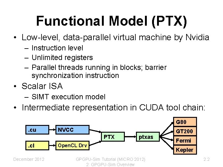
Functional Model (PTX) • Low-level, data-parallel virtual machine by Nvidia – Instruction level – Unlimited registers – Parallel threads running in blocks; barrier synchronization instruction • Scalar ISA – SIMT execution model • Intermediate representation in CUDA tool chain: G 80. cu NVCC PTX . cl December 2012 ptxas Open. CL Drv GPGPU-Sim Tutorial (MICRO 2012) 2: GPGPU-Sim Overview GT 200 Fermi Kepler 2. 2
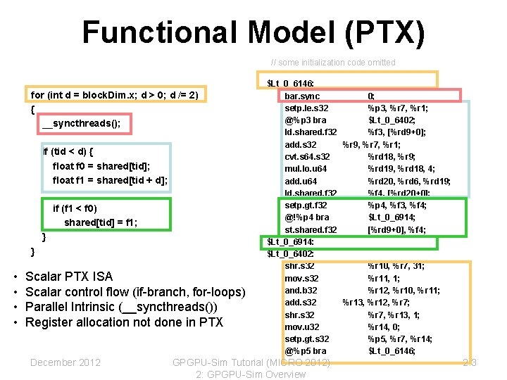
Functional Model (PTX) // some initialization code omitted for (int d = block. Dim. x; d > 0; d /= 2) { __syncthreads(); if (tid < d) { float f 0 = shared[tid]; float f 1 = shared[tid + d]; if (f 1 < f 0) shared[tid] = f 1; } } • • Scalar PTX ISA Scalar control flow (if-branch, for-loops) Parallel Intrinsic (__syncthreads()) Register allocation not done in PTX December 2012 $Lt_0_6146: bar. sync 0; setp. le. s 32 %p 3, %r 7, %r 1; @%p 3 bra $Lt_0_6402; ld. shared. f 32 %f 3, [%rd 9+0]; add. s 32 %r 9, %r 7, %r 1; cvt. s 64. s 32 %rd 18, %r 9; mul. lo. u 64 %rd 19, %rd 18, 4; add. u 64 %rd 20, %rd 6, %rd 19; ld. shared. f 32 %f 4, [%rd 20+0]; setp. gt. f 32 %p 4, %f 3, %f 4; @!%p 4 bra $Lt_0_6914; st. shared. f 32 [%rd 9+0], %f 4; $Lt_0_6914: $Lt_0_6402: shr. s 32 %r 10, %r 7, 31; mov. s 32 %r 11, 1; and. b 32 %r 12, %r 10, %r 11; add. s 32 %r 13, %r 12, %r 7; shr. s 32 %r 7, %r 13, 1; mov. u 32 %r 14, 0; setp. gt. s 32 %p 5, %r 7, %r 14; @%p 5 bra $Lt_0_6146; GPGPU-Sim Tutorial (MICRO 2012) 2: GPGPU-Sim Overview 2. 3
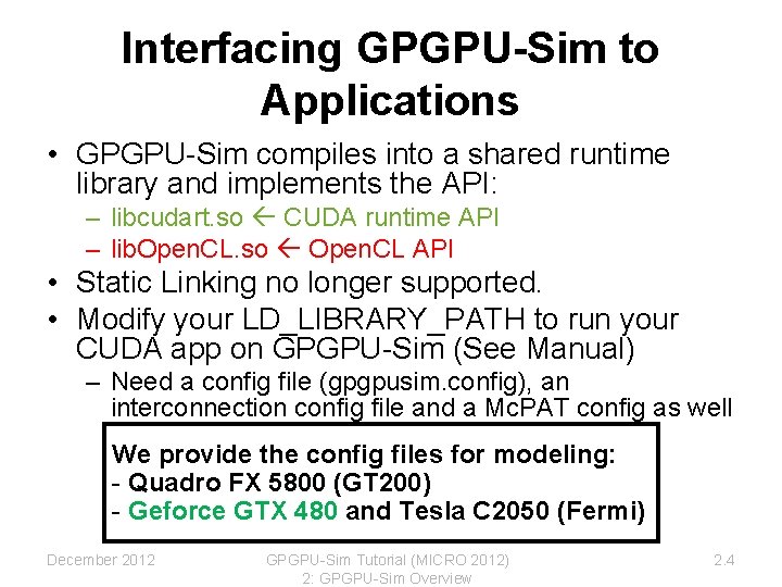
Interfacing GPGPU-Sim to Applications • GPGPU-Sim compiles into a shared runtime library and implements the API: – libcudart. so CUDA runtime API – lib. Open. CL. so Open. CL API • Static Linking no longer supported. • Modify your LD_LIBRARY_PATH to run your CUDA app on GPGPU-Sim (See Manual) – Need a config file (gpgpusim. config), an interconnection config file and a Mc. PAT config as well We provide the config files for modeling: - Quadro FX 5800 (GT 200) - Geforce GTX 480 and Tesla C 2050 (Fermi) December 2012 GPGPU-Sim Tutorial (MICRO 2012) 2: GPGPU-Sim Overview 2. 4
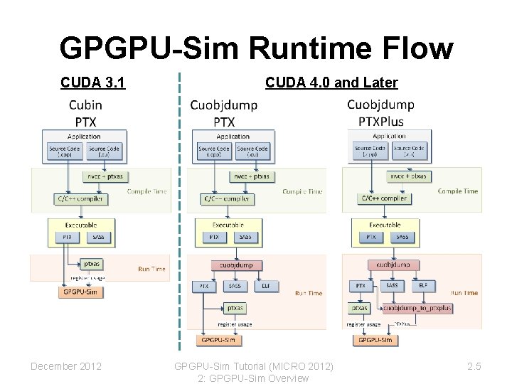
GPGPU-Sim Runtime Flow CUDA 3. 1 December 2012 CUDA 4. 0 and Later GPGPU-Sim Tutorial (MICRO 2012) 2: GPGPU-Sim Overview 2. 5
Debugging and Visualization • GPGPU-Sim provides tools to debug and visualize simulated GPU behavior. – GDB macros: Cycle-level debugging – Aerial. Vision: High-level performance dynamics December 2012 GPGPU-Sim Tutorial (MICRO 2012) 2: GPGPU-Sim Overview 2. 6
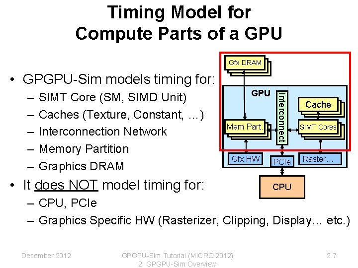
Timing Model for Compute Parts of a GPU Gfx DRAM • GPGPU-Sim models timing for: SIMT Core (SM, SIMD Unit) Caches (Texture, Constant, …) Interconnection Network Memory Partition Graphics DRAM GPU Mem Part. Gfx HW • It does NOT model timing for: Interconnect – – – PCIe Cache SIMT Cores Raster… CPU – CPU, PCIe – Graphics Specific HW (Rasterizer, Clipping, Display… etc. ) December 2012 GPGPU-Sim Tutorial (MICRO 2012) 2: GPGPU-Sim Overview 2. 7
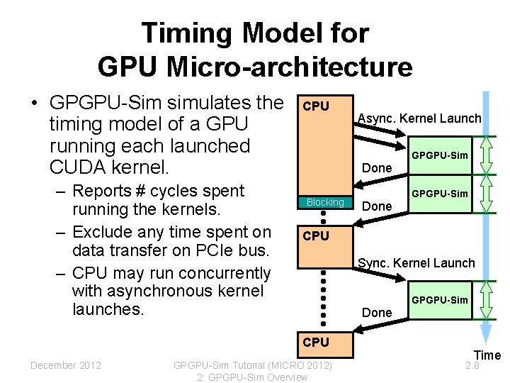
Timing Model for GPU Micro-architecture • GPGPU-Sim simulates the timing model of a GPU running each launched CUDA kernel. – Reports # cycles spent running the kernels. – Exclude any time spent on data transfer on PCIe bus. – CPU may run concurrently with asynchronous kernel launches. CPU Done Blocking Done GPGPU-Sim GPU HW CPU Sync. Kernel Launch Done CPU December 2012 Async. Kernel Launch GPGPU-Sim Tutorial (MICRO 2012) 2: GPGPU-Sim Overview GPGPU-Sim GPU HW Time 2. 8
Timing Model for GPU Micro-architecture • GPGPU-Sim is a detailed cycle-level simulator: – Cycle-level model for each part of the microarchitecture – Research focused • Ignoring rare corner cases to reduce complexity – CUDA manual provides some hints. NVIDIA IEEE Micro articles provide other hints. In most cases we can only guess at details. Guesses “informed” by studying patents and microbenchmarking. GPGPU-Sim w/ SASS is ~0. 98 correlated to the real HW. December 2012 GPGPU-Sim Tutorial (MICRO 2012) 2: GPGPU-Sim Overview 2. 9
Timing Model Overview • What is a warp? • SIMT Core Internals – SIMT Frontend – Memory Unit • Interconnection Network • Clock Domains • Memory Partition – DRAM Timing Model December 2012 GPGPU-Sim Tutorial (MICRO 2012) 4: Microarchitecture Model 4. 10
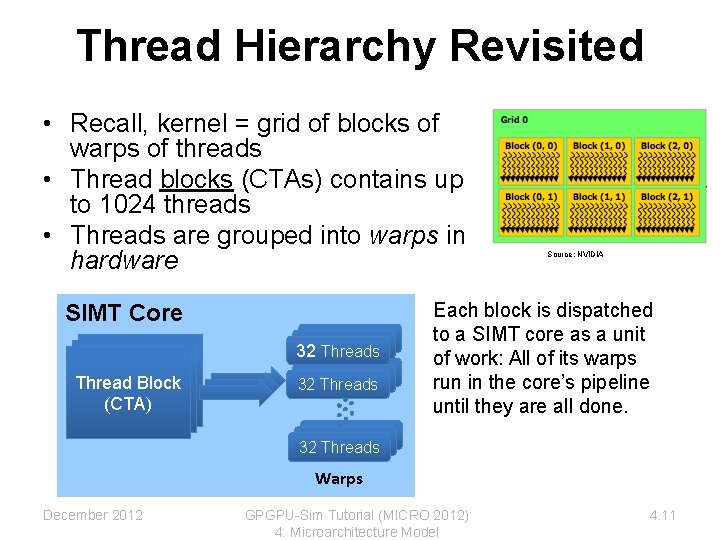
Thread Hierarchy Revisited • Recall, kernel = grid of blocks of warps of threads • Thread blocks (CTAs) contains up to 1024 threads • Threads are grouped into warps in hardware SIMT Core Thread. Block Thread Block (CTA) 32 Threads 32 32 Threads Source: NVIDIA Each block is dispatched to a SIMT core as a unit of work: All of its warps run in the core’s pipeline until they are all done. 32 Threads 32 32 Threads Warps December 2012 GPGPU-Sim Tutorial (MICRO 2012) 4: Microarchitecture Model 4. 11
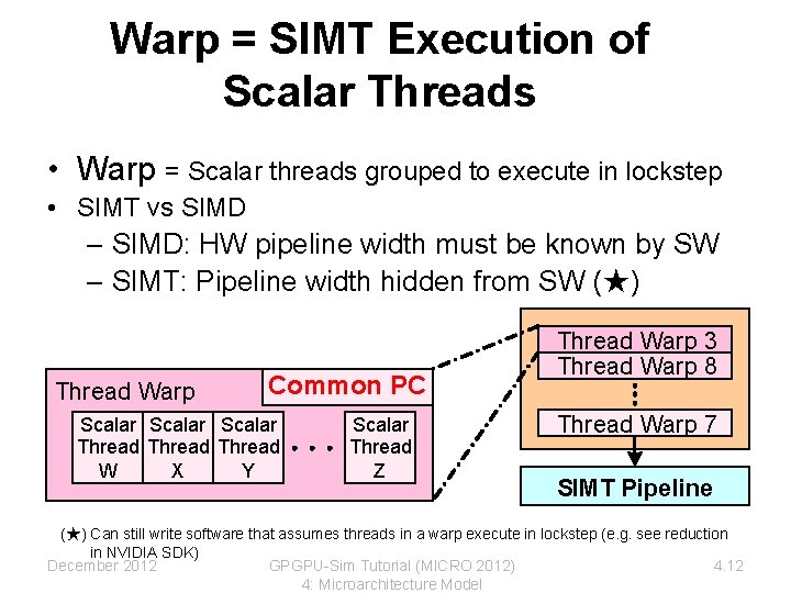
Warp = SIMT Execution of Scalar Threads • Warp = Scalar threads grouped to execute in lockstep • SIMT vs SIMD – SIMD: HW pipeline width must be known by SW – SIMT: Pipeline width hidden from SW (★) Thread Warp Common PC Scalar Thread W X Y Scalar Thread Z Thread Warp 3 Thread Warp 8 Thread Warp 7 SIMT Pipeline (★) Can still write software that assumes threads in a warp execute in lockstep (e. g. see reduction in NVIDIA SDK) December 2012 GPGPU-Sim Tutorial (MICRO 2012) 4. 12 4: Microarchitecture Model
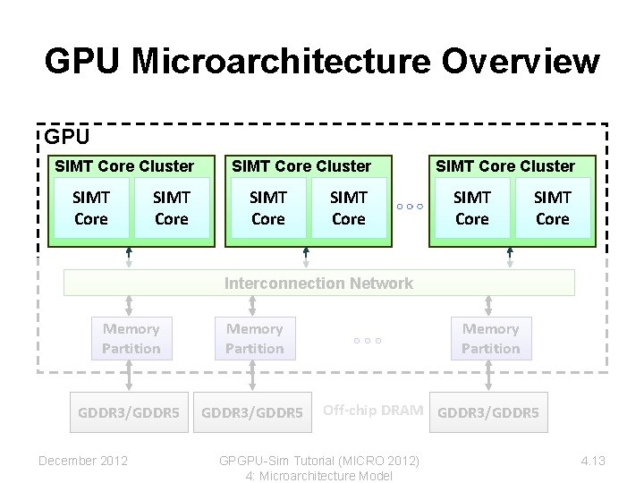
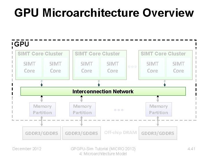
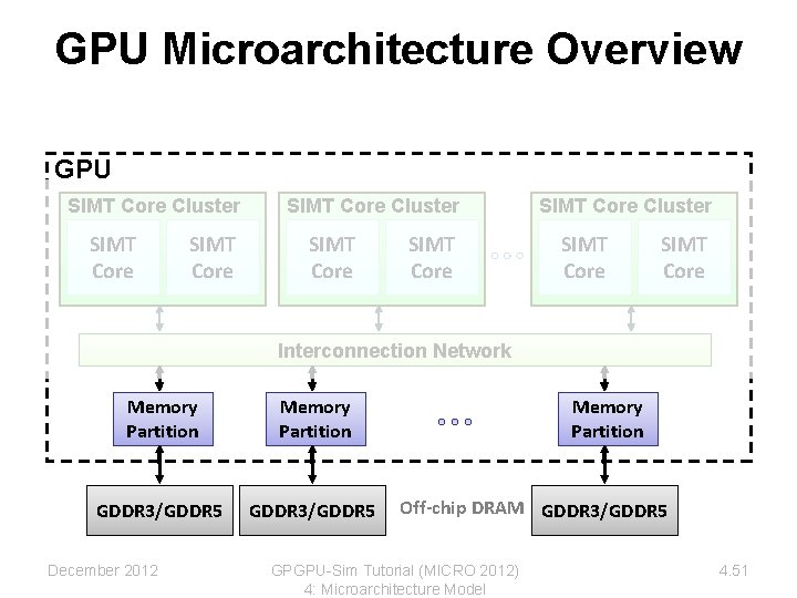
GPU Microarchitecture Overview GPU SIMT Core Cluster SIMT Core SIMT Core Cluster SIMT Core Interconnection Network Memory Partition GDDR 3/GDDR 5 December 2012 Memory Partition Off-chip DRAM GDDR 3/GDDR 5 GPGPU-Sim Tutorial (MICRO 2012) 4: Microarchitecture Model 4. 13
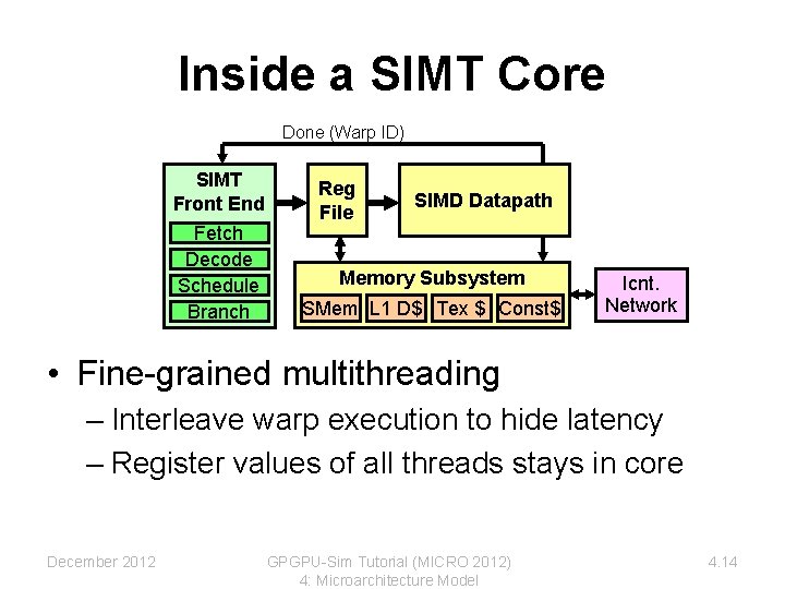
Inside a SIMT Core Done (Warp ID) SIMT Front End Fetch Decode Schedule Branch Reg File SIMD Datapath Memory Subsystem SMem L 1 D$ Tex $ Const$ Icnt. Network • Fine-grained multithreading – Interleave warp execution to hide latency – Register values of all threads stays in core December 2012 GPGPU-Sim Tutorial (MICRO 2012) 4: Microarchitecture Model 4. 14
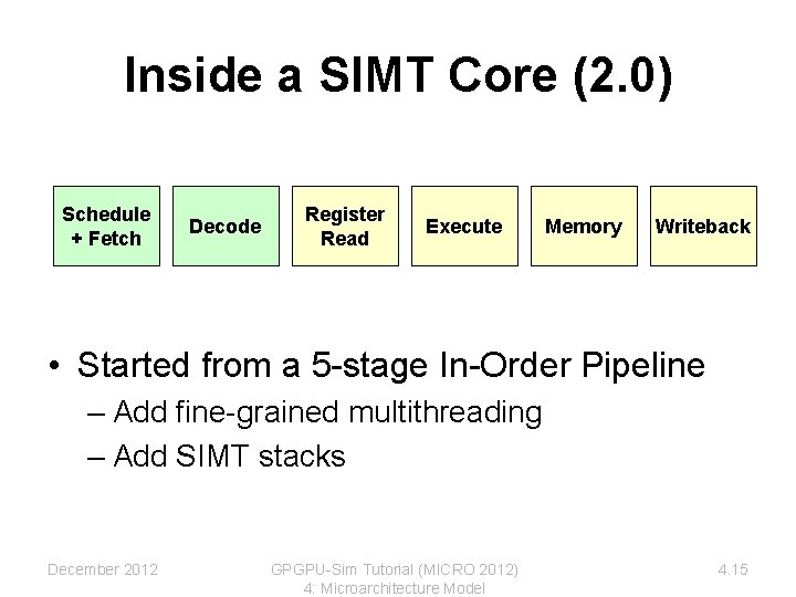
Inside a SIMT Core (2. 0) Schedule + Fetch Decode Register Read Execute Memory Writeback • Started from a 5 -stage In-Order Pipeline – Add fine-grained multithreading – Add SIMT stacks December 2012 GPGPU-Sim Tutorial (MICRO 2012) 4: Microarchitecture Model 4. 15
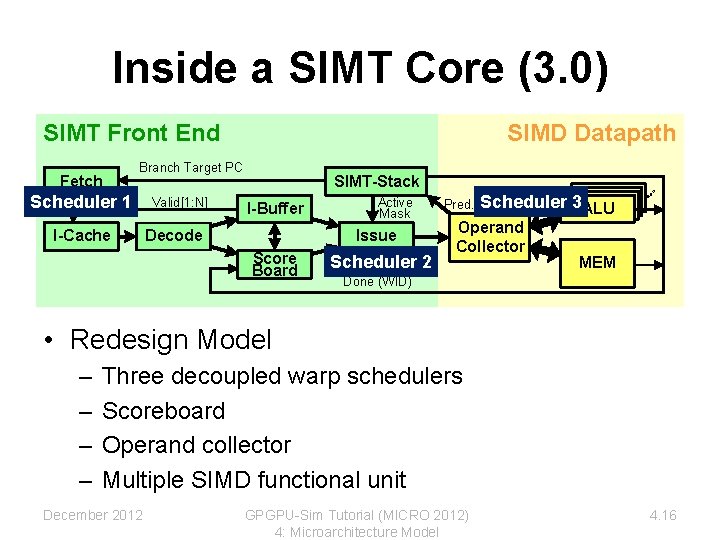
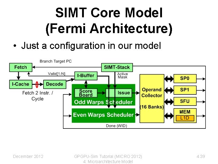
Inside a SIMT Core (3. 0) SIMT Front End Fetch SIMD Datapath Branch Target PC Scheduler 1 I-Cache Valid[1: N] SIMT-Stack I-Buffer Decode Active Mask Issue Score Board Scheduler 2 Pred. ALU Scheduler 3 ALU Operand Collector MEM Done (WID) • Redesign Model – – Three decoupled warp schedulers Scoreboard Operand collector Multiple SIMD functional unit December 2012 GPGPU-Sim Tutorial (MICRO 2012) 4: Microarchitecture Model 4. 16
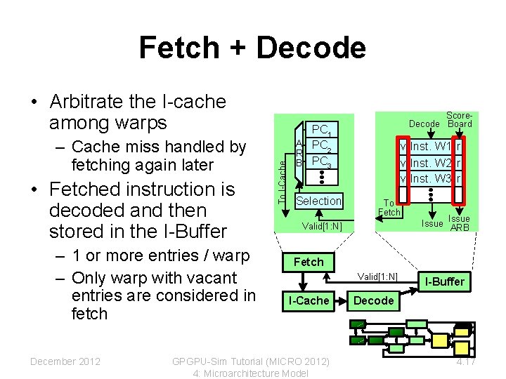
Fetch + Decode – Cache miss handled by fetching again later • Fetched instruction is decoded and then stored in the I-Buffer – 1 or more entries / warp – Only warp with vacant entries are considered in fetch December 2012 To I-Cache • Arbitrate the I-cache among warps Score. Decode Board PC 1 A PC 2 R B PC 3 Selection v Inst. W 1 r v Inst. W 2 r v Inst. W 3 r To Fetch Valid[1: N] Issue ARB Fetch Valid[1: N] I-Cache GPGPU-Sim Tutorial (MICRO 2012) 4: Microarchitecture Model I-Buffer Decode 4. 17
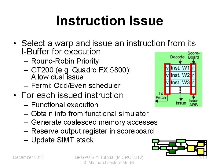
Instruction Issue • Select a warp and issue an instruction from its I-Buffer for execution – Round-Robin Priority – GT 200 (e. g. Quadro FX 5800): Allow dual issue – Fermi: Odd/Even scheduler • For each issued instruction: – – – Functional execution Obtain info from functional simulator Generate coalesced memory accesses Reserve output register in scoreboard Update SIMT stack December 2012 GPGPU-Sim Tutorial (MICRO 2012) 4: Microarchitecture Model 4. 18
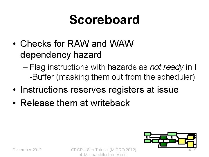
Scoreboard • Checks for RAW and WAW dependency hazard – Flag instructions with hazards as not ready in I -Buffer (masking them out from the scheduler) • Instructions reserves registers at issue • Release them at writeback December 2012 GPGPU-Sim Tutorial (MICRO 2012) 4: Microarchitecture Model 4. 19
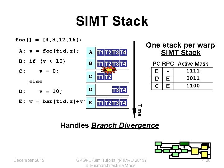
SIMT Stack foo[] = {4, 8, 12, 16}; A: v = foo[tid. x]; A T 1 T 2 T 3 T 4 B: if (v < 10) B T 1 T 2 T 3 T 4 C: v = 0; PC RPC Active Mask 1111 B E 0011 D E 1100 C E C T 1 T 2 else D: One stack per warp SIMT Stack v = 10; D T 3 T 4 Time E: w = bar[tid. x]+v; E T 1 T 2 T 3 T 4 Handles Branch Divergence December 2012 GPGPU-Sim Tutorial (MICRO 2012) 4: Microarchitecture Model 4. 20
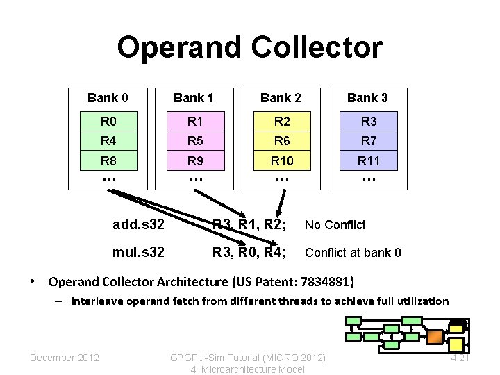
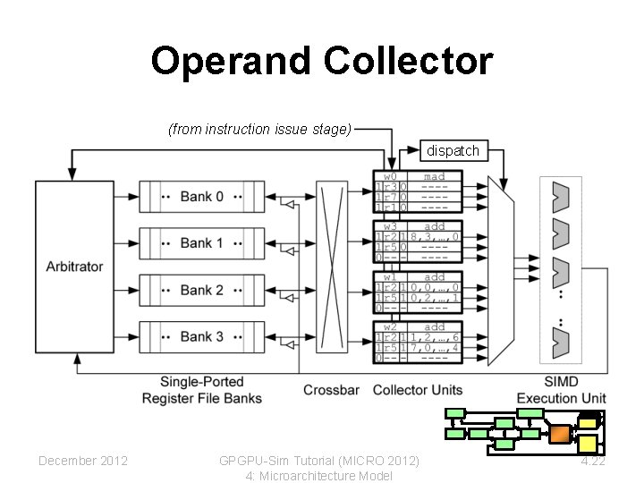
Operand Collector Bank 0 Bank 1 Bank 2 Bank 3 R 0 R 1 R 2 R 3 R 4 R 5 R 6 R 7 R 8 … R 9 … R 10 … R 11 … add. s 32 R 3, R 1, R 2; No Conflict mul. s 32 R 3, R 0, R 4; Conflict at bank 0 • Operand Collector Architecture (US Patent: 7834881) – Interleave operand fetch from different threads to achieve full utilization December 2012 GPGPU-Sim Tutorial (MICRO 2012) 4: Microarchitecture Model 4. 21
Operand Collector (from instruction issue stage) dispatch December 2012 GPGPU-Sim Tutorial (MICRO 2012) 4: Microarchitecture Model 4. 22
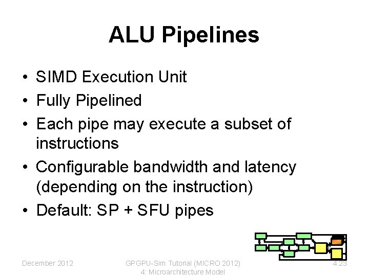
ALU Pipelines • SIMD Execution Unit • Fully Pipelined • Each pipe may execute a subset of instructions • Configurable bandwidth and latency (depending on the instruction) • Default: SP + SFU pipes December 2012 GPGPU-Sim Tutorial (MICRO 2012) 4: Microarchitecture Model 4. 23
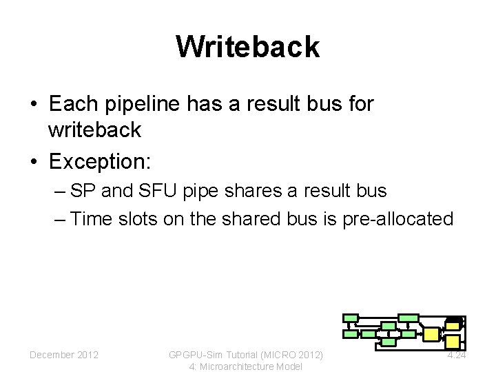
Writeback • Each pipeline has a result bus for writeback • Exception: – SP and SFU pipe shares a result bus – Time slots on the shared bus is pre-allocated December 2012 GPGPU-Sim Tutorial (MICRO 2012) 4: Microarchitecture Model 4. 24
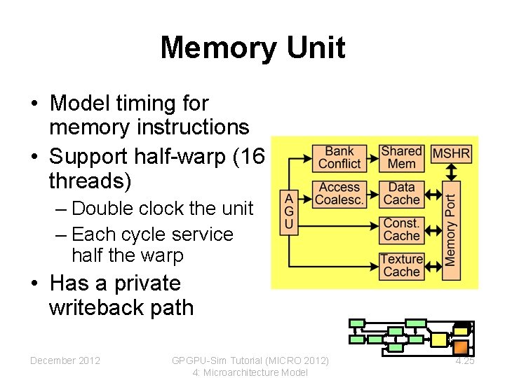
Memory Unit • Model timing for memory instructions • Support half-warp (16 threads) – Double clock the unit – Each cycle service half the warp • Has a private writeback path December 2012 GPGPU-Sim Tutorial (MICRO 2012) 4: Microarchitecture Model 4. 25
Constant Cache • A Read-only cache for constant memory • GPGPU-Sim simulates 1 read ports – A warp can access 1 constant cache locations in a single memory unit cycle – If more than 1 locations accessed • reads are serialized causing pipeline stalls – # of ports is not configurable December 2012 GPGPU-Sim Tutorial (MICRO 2012) 4: Microarchitecture Model 4. 26
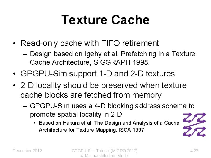
Texture Cache • Read-only cache with FIFO retirement – Design based on Igehy et al. Prefetching in a Texture Cache Architecture, SIGGRAPH 1998. • GPGPU-Sim support 1 -D and 2 -D textures • 2 -D locality should be preserved when texture cache blocks are fetched from memory – GPGPU-Sim uses a 4 -D blocking address scheme to promote spatial locality in 2 -D • Based on Hakura et al. The Design and Analysis of a Cache Architecture for Texture Mapping, ISCA 1997 December 2012 GPGPU-Sim Tutorial (MICRO 2012) 4: Microarchitecture Model 4. 27
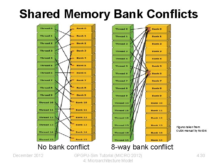
Shared Memory • Explicitly managed scratchpad memory – As fast as register files in absence of bank conflicts • Threads in a block can cooperate via shared memory • Each SIMT core has its own shared memory – Dynamically allocated to thread blocks • 16 k. B/48 k. B per SIMT core in current NVIDIA GPUs (Fermi) December 2012 GPGPU-Sim Tutorial (MICRO 2012) 4: Microarchitecture Model 4. 28
Shared Memory (cont. ) • Many threads accessing memory – Therefore Shared memory is highly banked • Each bank serves one address per cycle • Multiple access to a bank in a single cycle cause bank conflicts – Conflicting accesses must be serialized • Shared memory in NVIDIA GPUs has 16/32 banks – Configurable in GPGPU-Sim (version 3. 1. 2) December 2012 GPGPU-Sim Tutorial (MICRO 2012) 4: Microarchitecture Model 4. 29
Shared Memory Bank Conflicts Figures taken from CUDA manual by NVIDIA No bank conflict December 2012 8 -way bank conflict GPGPU-Sim Tutorial (MICRO 2012) 4: Microarchitecture Model 4. 30
Global Memory • Global memory is the off-chip DRAM memory – The largest and slowest memory available – Accesses must go through interconnect, memory partition and off-chip DRAM – Optionally cached in HW • L 1 Data Cache • L 2 Unified Cache December 2012 GPGPU-Sim Tutorial (MICRO 2012) 4: Microarchitecture Model 4. 31
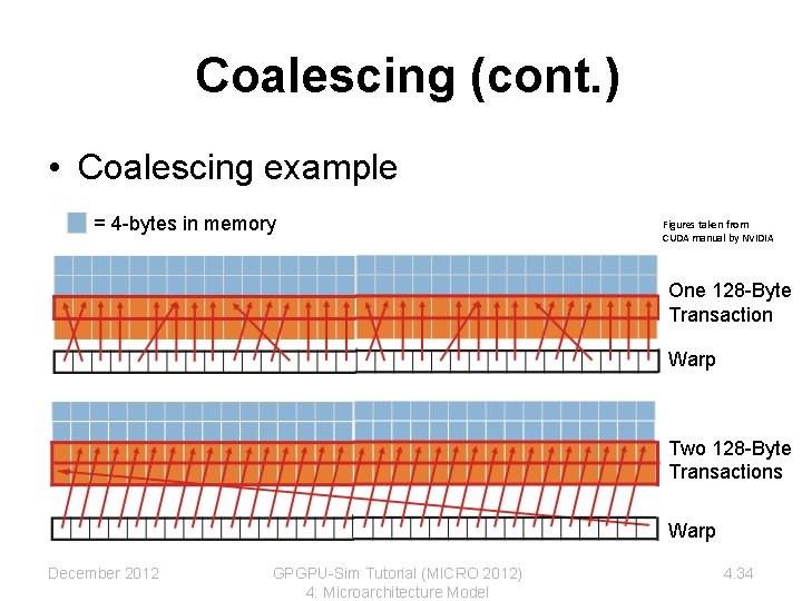
Coalescing • Combining memory accesses made by threads in a warp into fewer transactions – E. g. if threads in a warp are accessing consecutive 4 -byte sized locations in memory • Send one 128–byte request to DRAM (coalescing) • Instead of 32 4 -byte requests • This reduces the number of transactions between SIMT cores and DRAM – Less work for Interconnect, Memory Partition and DRAM December 2012 GPGPU-Sim Tutorial (MICRO 2012) 4: Microarchitecture Model 4. 32
Coalescing (Cont. ) • CUDA Capability 1. 3 (e. g. GTX 280) – Coalescing done per half-warp – Can create 128 -byte, 64 -byte or 32 -byte transactions • CUDA Capability 2. 0 (e. g. Fermi) – Coalescing done for a full warp – Cached: Only creates 128 -byte transactions – Not Cached: Can create 128/64/32 -byte transactions • GPGPU-Sim supports both December 2012 GPGPU-Sim Tutorial (MICRO 2012) 4: Microarchitecture Model 4. 33
Coalescing (cont. ) • Coalescing example = 4 -bytes in memory Figures taken from CUDA manual by NVIDIA One 128 -Byte Transaction Warp Two 128 -Byte Transactions Warp December 2012 GPGPU-Sim Tutorial (MICRO 2012) 4: Microarchitecture Model 4. 34
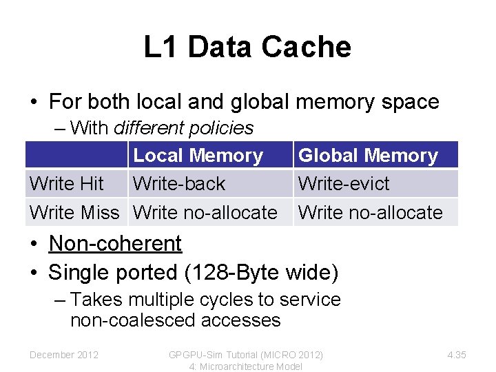
L 1 Data Cache • For both local and global memory space – With different policies Local Memory Write Hit Write-back Write Miss Write no-allocate Global Memory Write-evict Write no-allocate • Non-coherent • Single ported (128 -Byte wide) – Takes multiple cycles to service non-coalesced accesses December 2012 GPGPU-Sim Tutorial (MICRO 2012) 4: Microarchitecture Model 4. 35
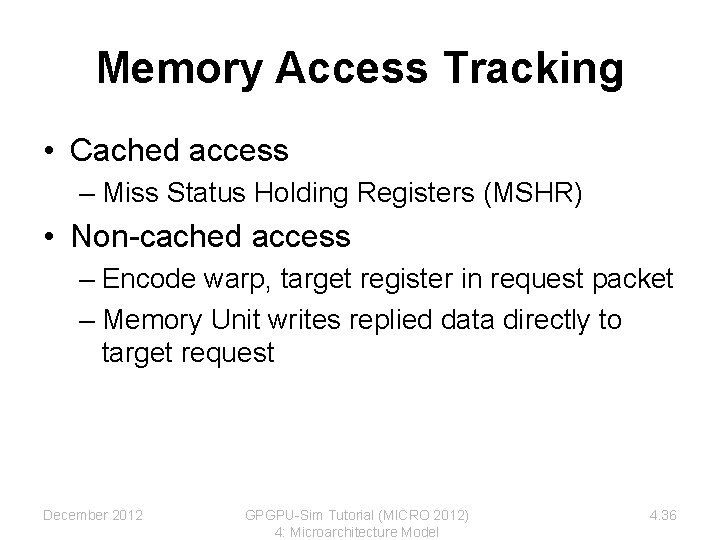
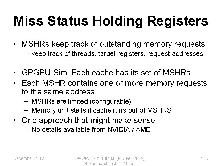
Memory Access Tracking • Cached access – Miss Status Holding Registers (MSHR) • Non-cached access – Encode warp, target register in request packet – Memory Unit writes replied data directly to target request December 2012 GPGPU-Sim Tutorial (MICRO 2012) 4: Microarchitecture Model 4. 36
Miss Status Holding Registers • MSHRs keep track of outstanding memory requests – keep track of threads, target registers, request addresses • GPGPU-Sim: Each cache has its set of MSHRs • Each MSHR contains one or more memory requests to the same address – MSHRs are limited (configurable) – Memory unit stalls if cache runs out of MSHRS • One approach that might make sense – No details available from NVIDIA / AMD December 2012 GPGPU-Sim Tutorial (MICRO 2012) 4: Microarchitecture Model 4. 37
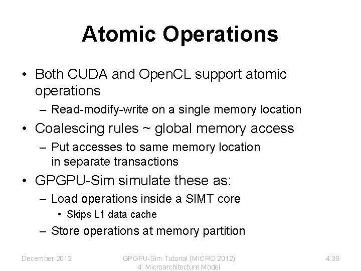
Atomic Operations • Both CUDA and Open. CL support atomic operations – Read-modify-write on a single memory location • Coalescing rules ~ global memory access – Put accesses to same memory location in separate transactions • GPGPU-Sim simulate these as: – Load operations inside a SIMT core • Skips L 1 data cache – Store operations at memory partition December 2012 GPGPU-Sim Tutorial (MICRO 2012) 4: Microarchitecture Model 4. 38
SIMT Core Model (Fermi Architecture) • Just a configuration in our model December 2012 GPGPU-Sim Tutorial (MICRO 2012) 4: Microarchitecture Model 4. 39
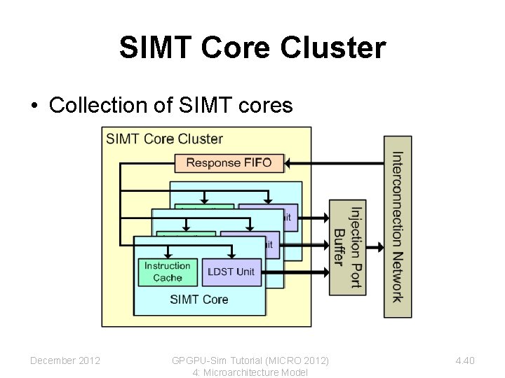
SIMT Core Cluster • Collection of SIMT cores December 2012 GPGPU-Sim Tutorial (MICRO 2012) 4: Microarchitecture Model 4. 40
GPU Microarchitecture Overview GPU SIMT Core Cluster SIMT Core SIMT Core Cluster SIMT Core Interconnection Network Memory Partition GDDR 3/GDDR 5 December 2012 Memory Partition Off-chip DRAM GDDR 3/GDDR 5 GPGPU-Sim Tutorial (MICRO 2012) 4: Microarchitecture Model 4. 41
Clock domains • Simulate independent clock domains for – SIMT cores • GT 200: Set to ¼ of shader clock to compensate for using SIMD width of 32 instead of 8 • Fermi: Set to ½ of shader clock to compensate for using SIMD width of 32 instead of 16 – Interconnection network – L 2 cache (if enabled) – DRAM • This is real clock (command clock) • Effective clock is 2 x this clock due to DDR December 2012 GPGPU-Sim Tutorial (MICRO 2012) 4: Microarchitecture Model 4. 42
Clock Domain Crossing • We simulate send and receive buffers at clock crossing boundaries • The buffers are filled and drained in different clock domains • E. g. consider the buffer from interconnect to memory partition – Filled at interconnect clock rate – Drained at DRAM clock rate December 2012 GPGPU-Sim Tutorial (MICRO 2012) 4: Microarchitecture Model 4. 43
Interconnection Network Model • Intersim (Booksim) a flit level simulator – Topologies (Mesh, Torus, Butterfly, …) – Routing (Dimension Order, Adaptive, etc. ) – Flow Control (Virtual Channels, Credits) • We simulate two separate networks – From SIMT cores to memory partitions • Read Requests, Write Requests – From memory partitions to SIMT cores • Read Replies, Write Acks December 2012 GPGPU-Sim Tutorial (MICRO 2012) 4: Microarchitecture Model 4. 44
Topology Examples December 2012 GPGPU-Sim Tutorial (MICRO 2012) 4: Microarchitecture Model 4. 45
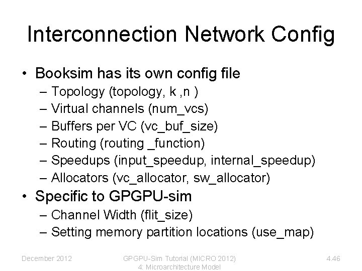
Interconnection Network Config • Booksim has its own config file – Topology (topology, k , n ) – Virtual channels (num_vcs) – Buffers per VC (vc_buf_size) – Routing (routing _function) – Speedups (input_speedup, internal_speedup) – Allocators (vc_allocator, sw_allocator) • Specific to GPGPU-sim – Channel Width (flit_size) – Setting memory partition locations (use_map) December 2012 GPGPU-Sim Tutorial (MICRO 2012) 4: Microarchitecture Model 4. 46
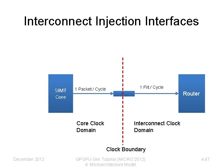
Interconnect Injection Interfaces SIMT Core 1 Packet / Cycle Core Clock Domain 1 Flit / Cycle Router Interconnect Clock Domain Clock Boundary December 2012 GPGPU-Sim Tutorial (MICRO 2012) 4: Microarchitecture Model 4. 47
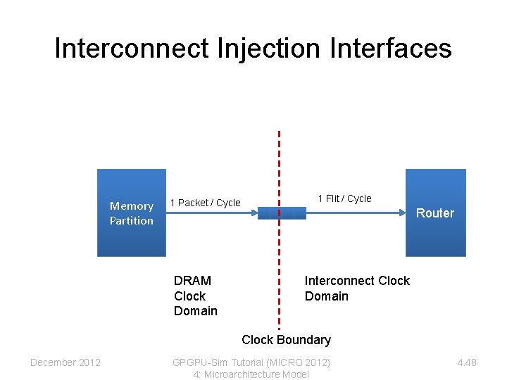
Interconnect Injection Interfaces Memory Partition 1 Packet / Cycle DRAM Clock Domain 1 Flit / Cycle Router Interconnect Clock Domain Clock Boundary December 2012 GPGPU-Sim Tutorial (MICRO 2012) 4: Microarchitecture Model 4. 48
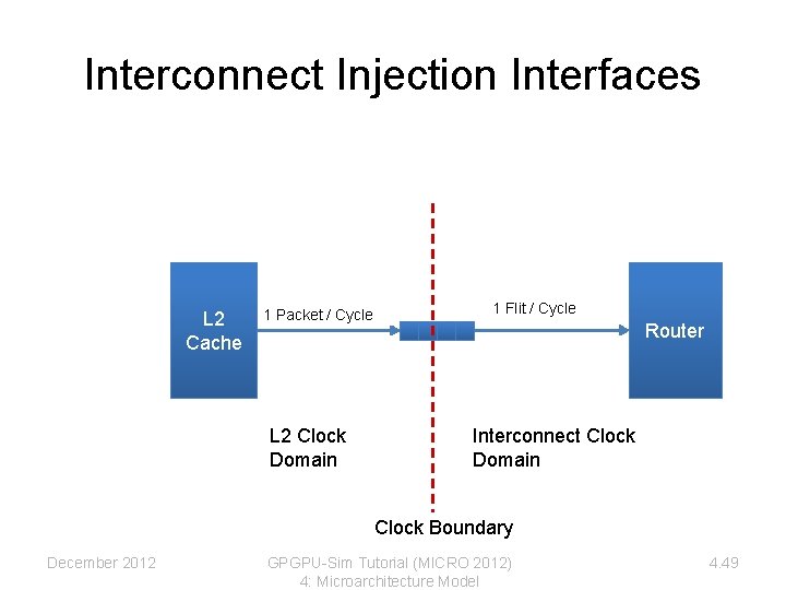
Interconnect Injection Interfaces L 2 Cache 1 Packet / Cycle L 2 Clock Domain 1 Flit / Cycle Router Interconnect Clock Domain Clock Boundary December 2012 GPGPU-Sim Tutorial (MICRO 2012) 4: Microarchitecture Model 4. 49
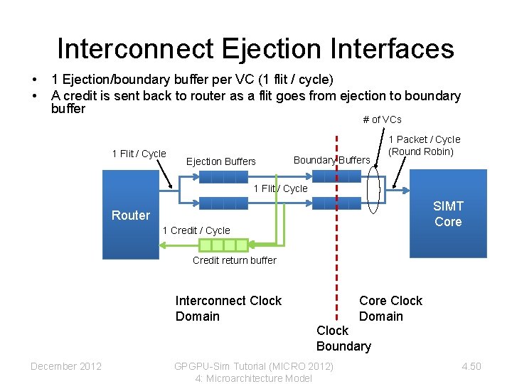
Interconnect Ejection Interfaces • • 1 Ejection/boundary buffer per VC (1 flit / cycle) A credit is sent back to router as a flit goes from ejection to boundary buffer # of VCs 1 Flit / Cycle Ejection Buffers Boundary Buffers 1 Packet / Cycle (Round Robin) 1 Flit / Cycle SIMT Core Router 1 Credit / Cycle Credit return buffer Interconnect Clock Domain Core Clock Domain Clock Boundary December 2012 GPGPU-Sim Tutorial (MICRO 2012) 4: Microarchitecture Model 4. 50
GPU Microarchitecture Overview GPU SIMT Core Cluster SIMT Core SIMT Core Cluster SIMT Core Interconnection Network Memory Partition GDDR 3/GDDR 5 December 2012 Memory Partition Off-chip DRAM GDDR 3/GDDR 5 GPGPU-Sim Tutorial (MICRO 2012) 4: Microarchitecture Model 4. 51
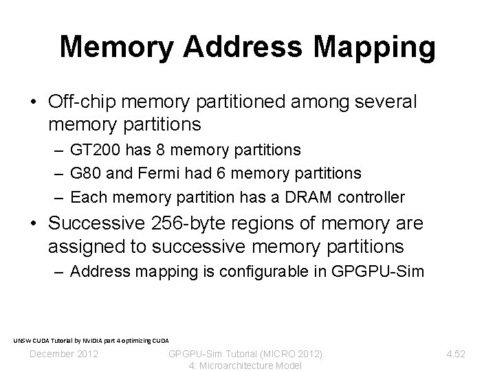
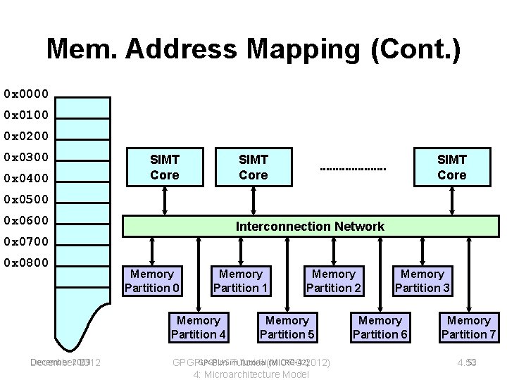
Memory Address Mapping • Off-chip memory partitioned among several memory partitions – GT 200 has 8 memory partitions – G 80 and Fermi had 6 memory partitions – Each memory partition has a DRAM controller • Successive 256 -byte regions of memory are assigned to successive memory partitions – Address mapping is configurable in GPGPU-Sim UNSW CUDA Tutorial by NVIDIA part 4 optimizing CUDA December 2012 GPGPU-Sim Tutorial (MICRO 2012) 4: Microarchitecture Model 4. 52
Mem. Address Mapping (Cont. ) 0 x 0000 0 x 0100 0 x 0200 0 x 0300 0 x 0400 SIMT Core 0 x 0500 0 x 0600 Interconnection Network 0 x 0700 0 x 0800 Memory Partition 1 Memory Partition 4 December 2009 2012 Memory Partition 5 GPGPU-Sim Tutorial(MICRO-42)2012) GPGPU-Sim Tutorial 4: Microarchitecture Model Memory Partition 3 Memory Partition 6 Memory Partition 7 53 4. 53
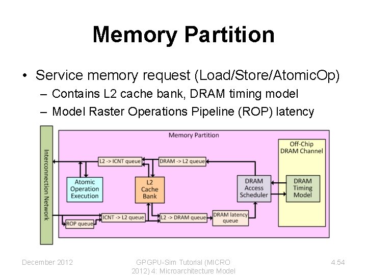
Memory Partition • Service memory request (Load/Store/Atomic. Op) – Contains L 2 cache bank, DRAM timing model – Model Raster Operations Pipeline (ROP) latency December 2012 GPGPU-Sim Tutorial (MICRO 2012) 4: Microarchitecture Model 4. 54
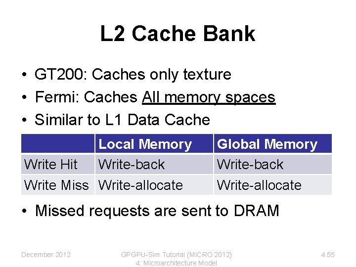
L 2 Cache Bank • GT 200: Caches only texture • Fermi: Caches All memory spaces • Similar to L 1 Data Cache Write Hit Local Memory Write-back Write Miss Write-allocate Global Memory Write-back Write-allocate • Missed requests are sent to DRAM December 2012 GPGPU-Sim Tutorial (MICRO 2012) 4: Microarchitecture Model 4. 55
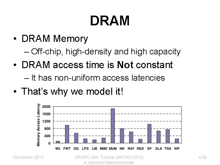
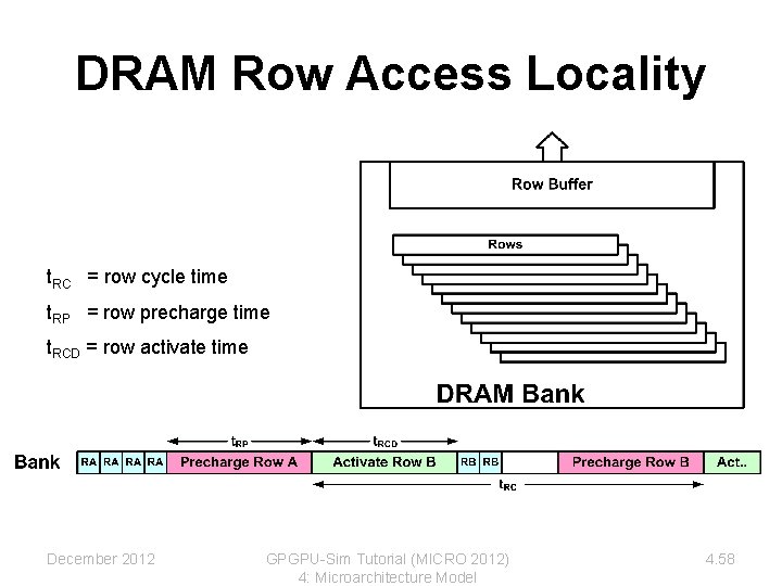
DRAM • DRAM Memory – Off-chip, high-density and high capacity • DRAM access time is Not constant – It has non-uniform access latencies • That’s why we model it! December 2012 GPGPU-Sim Tutorial (MICRO 2012) 4: Microarchitecture Model 4. 56
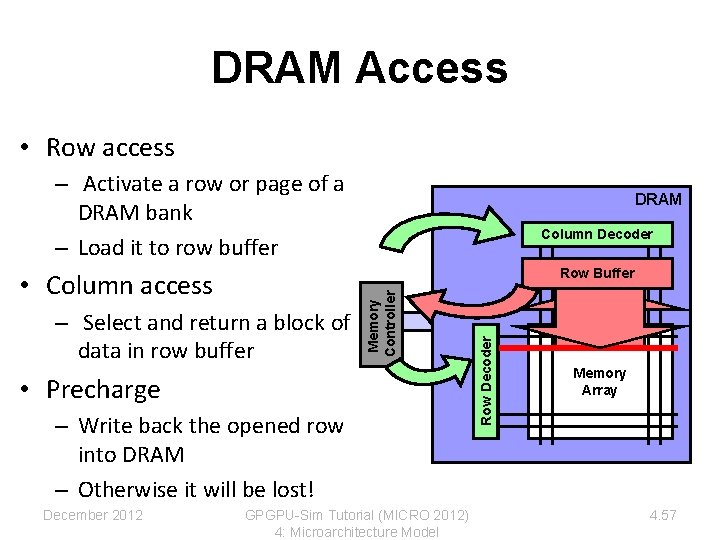
DRAM Access • Row access – Activate a row or page of a DRAM bank – Load it to row buffer DRAM Column Decoder – Select and return a block of data in row buffer • Precharge – Write back the opened row into DRAM – Otherwise it will be lost! December 2012 GPGPU-Sim Tutorial (MICRO 2012) 4: Microarchitecture Model Row Decoder • Column access Memory Controller Row Buffer Memory Array 4. 57
DRAM Row Access Locality t. RC = row cycle time t. RP = row precharge time t. RCD = row activate time December 2012 GPGPU-Sim Tutorial (MICRO 2012) 4: Microarchitecture Model 4. 58
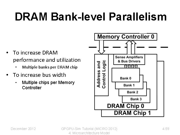
DRAM Bank-level Parallelism • To increase DRAM performance and utilization • Multiple banks per DRAM chip • To increase bus width • Multiple chips per Memory Controller December 2012 GPGPU-Sim Tutorial (MICRO 2012) 4: Microarchitecture Model 4. 59
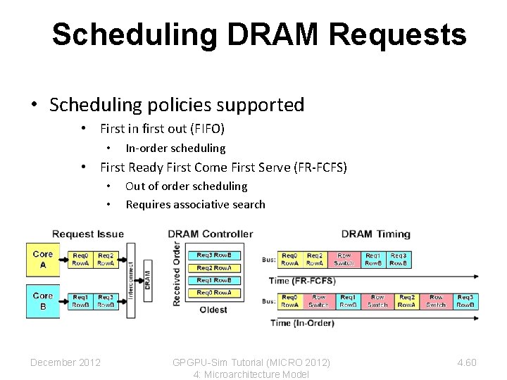
Scheduling DRAM Requests • Scheduling policies supported • First in first out (FIFO) • In-order scheduling • First Ready First Come First Serve (FR-FCFS) • • December 2012 Out of order scheduling Requires associative search GPGPU-Sim Tutorial (MICRO 2012) 4: Microarchitecture Model 4. 60
Session Summary • Microarchitecture Timing Model in GPGPU -Sim – SIMT Core – Cache Model – Interconnection Network – Memory Partition + Address Mapping – DRAM Scheduling and Timing December 2012 GPGPU-Sim Tutorial (MICRO 2012) 4: Microarchitecture Model 4. 61