Wet Etching and Cleaning Surface Considerations and Process
- Slides: 26

Wet Etching and Cleaning: Surface Considerations and Process Issues Dr. Srini Raghavan Dept. of Chemical and Environmental Engineering University of Arizona 1999 Arizona Board of Regents for The University of Arizona NSF/SRC Engineering Research Center for Environmentally Benign Semiconductor Manufacturing 1

Outline • Etching and cleaning solutions/processes • Particle adhesion theory • Surface charge and chemistry • Contamination NSF/SRC Engineering Research Center for Environmentally Benign Semiconductor Manufacturing 2

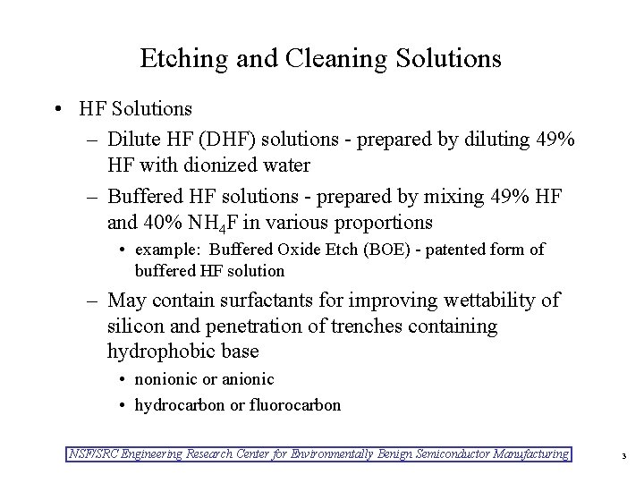
Etching and Cleaning Solutions • HF Solutions – Dilute HF (DHF) solutions - prepared by diluting 49% HF with dionized water – Buffered HF solutions - prepared by mixing 49% HF and 40% NH 4 F in various proportions • example: Buffered Oxide Etch (BOE) - patented form of buffered HF solution – May contain surfactants for improving wettability of silicon and penetration of trenches containing hydrophobic base • nonionic or anionic • hydrocarbon or fluorocarbon NSF/SRC Engineering Research Center for Environmentally Benign Semiconductor Manufacturing 3

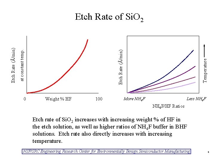
0 Weight % HF 100 Temperature Etch Rate (Å/min) at constant temp. Etch Rate (Å/min) Etch Rate of Si. O 2 More NH 4 F Less NH 4 F/HF Ratios Etch rate of Si. O 2 increases with increasing weight % of HF in the etch solution, as well as higher ratios of NH 4 F buffer in BHF solutions. Etch rate also directly increases with increasing temperature. NSF/SRC Engineering Research Center for Environmentally Benign Semiconductor Manufacturing 4

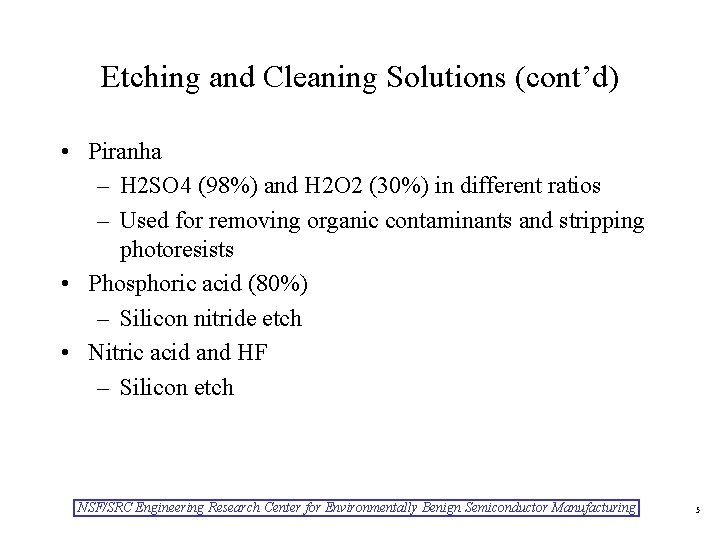
Etching and Cleaning Solutions (cont’d) • Piranha – H 2 SO 4 (98%) and H 2 O 2 (30%) in different ratios – Used for removing organic contaminants and stripping photoresists • Phosphoric acid (80%) – Silicon nitride etch • Nitric acid and HF – Silicon etch NSF/SRC Engineering Research Center for Environmentally Benign Semiconductor Manufacturing 5

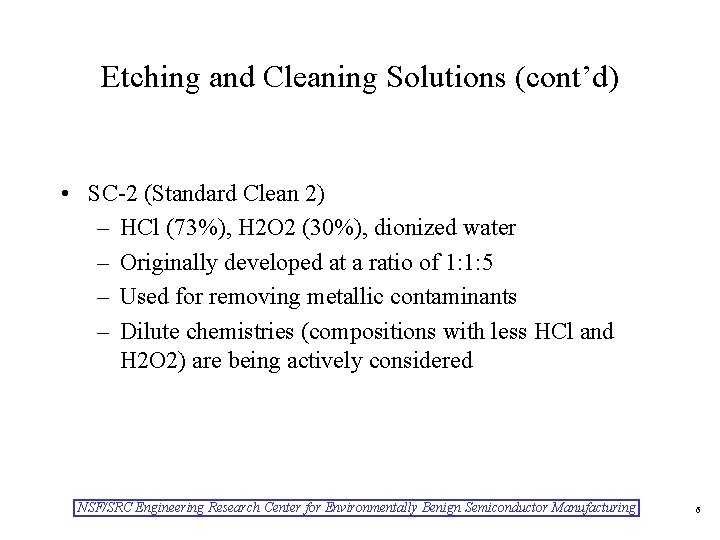
Etching and Cleaning Solutions (cont’d) • SC-2 (Standard Clean 2) – HCl (73%), H 2 O 2 (30%), dionized water – Originally developed at a ratio of 1: 1: 5 – Used for removing metallic contaminants – Dilute chemistries (compositions with less HCl and H 2 O 2) are being actively considered NSF/SRC Engineering Research Center for Environmentally Benign Semiconductor Manufacturing 6

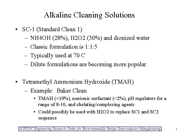
Alkaline Cleaning Solutions • SC-1 (Standard Clean 1) – NH 4 OH (28%), H 2 O 2 (30%) and dionized water – Classic formulation is 1: 1: 5 – Typically used at 70 C – Dilute formulations are becoming more popular • Tetramethyl Ammonium Hydroxide (TMAH) – Example: Baker Clean • TMAH (<10%), nonionic surfactant (<2%), p. H regulators for a range of 8 -10, and chelating/complexing agents • Could possibly be used with H 2 O 2 to replace SC 1 and SC 2 sequence NSF/SRC Engineering Research Center for Environmentally Benign Semiconductor Manufacturing 7

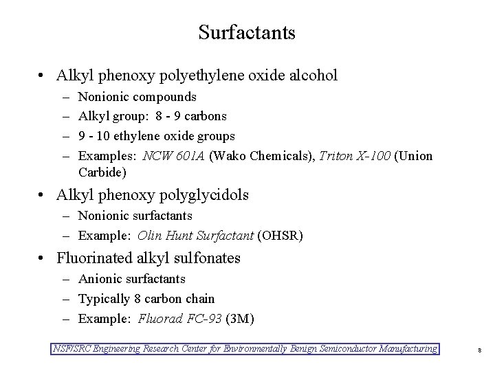
Surfactants • Alkyl phenoxy polyethylene oxide alcohol – – Nonionic compounds Alkyl group: 8 - 9 carbons 9 - 10 ethylene oxide groups Examples: NCW 601 A (Wako Chemicals), Triton X-100 (Union Carbide) • Alkyl phenoxy polyglycidols – Nonionic surfactants – Example: Olin Hunt Surfactant (OHSR) • Fluorinated alkyl sulfonates – Anionic surfactants – Typically 8 carbon chain – Example: Fluorad FC-93 (3 M) NSF/SRC Engineering Research Center for Environmentally Benign Semiconductor Manufacturing 8

Surfactants (cont’d) • Acetylenic alcohols – Unsaturated triple bond in the structure – Nonionic – Example: Surfynol 61 (APCI) • Betaines – Zwitterionic in nature – Used mostly in alkaline clean – Example: Cocoamidopropyl betaine NSF/SRC Engineering Research Center for Environmentally Benign Semiconductor Manufacturing 9

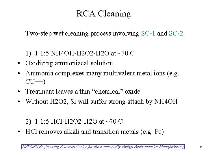
RCA Cleaning Two-step wet cleaning process involving SC-1 and SC-2: • • 1) 1: 1: 5 NH 4 OH-H 2 O 2 -H 2 O at ~70 C Oxidizing ammoniacal solution Ammonia complexes many multivalent metal ions (e. g. CU++) Treatment leaves a thin “chemical” oxide Without H 2 O 2, Si will suffer strong attach by NH 4 OH 2) 1: 1: 5 HCl-H 2 O 2 -H 2 O at ~70 C • HCl removes alkali and transition metals (e. g. Fe) NSF/SRC Engineering Research Center for Environmentally Benign Semiconductor Manufacturing 10

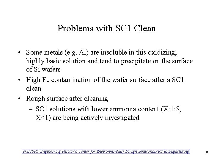
Problems with SC 1 Clean • Some metals (e. g. Al) are insoluble in this oxidizing, highly basic solution and tend to precipitate on the surface of Si wafers • High Fe contamination of the wafer surface after a SC 1 clean • Rough surface after cleaning – SC 1 solutions with lower ammonia content (X: 1: 5, X<1) are being actively investigated NSF/SRC Engineering Research Center for Environmentally Benign Semiconductor Manufacturing 11

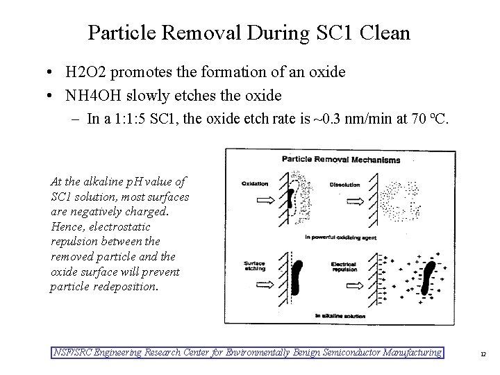
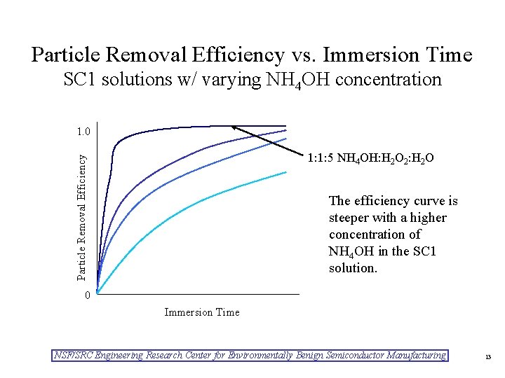
Particle Removal During SC 1 Clean • H 2 O 2 promotes the formation of an oxide • NH 4 OH slowly etches the oxide – In a 1: 1: 5 SC 1, the oxide etch rate is ~0. 3 nm/min at 70 ºC. At the alkaline p. H value of SC 1 solution, most surfaces are negatively charged. Hence, electrostatic repulsion between the removed particle and the oxide surface will prevent particle redeposition. NSF/SRC Engineering Research Center for Environmentally Benign Semiconductor Manufacturing 12

Particle Removal Efficiency vs. Immersion Time SC 1 solutions w/ varying NH 4 OH concentration 1. 0 Particle Removal Efficiency 1: 1: 5 NH 4 OH: H 2 O 2: H 2 O The efficiency curve is steeper with a higher concentration of NH 4 OH in the SC 1 solution. 0 Immersion Time NSF/SRC Engineering Research Center for Environmentally Benign Semiconductor Manufacturing 13

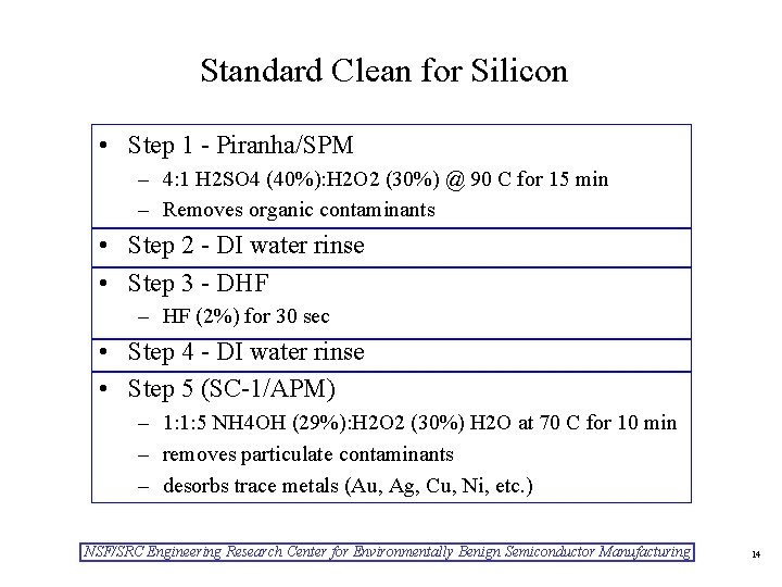
Standard Clean for Silicon • Step 1 - Piranha/SPM – 4: 1 H 2 SO 4 (40%): H 2 O 2 (30%) @ 90 C for 15 min – Removes organic contaminants • Step 2 - DI water rinse • Step 3 - DHF – HF (2%) for 30 sec • Step 4 - DI water rinse • Step 5 (SC-1/APM) – 1: 1: 5 NH 4 OH (29%): H 2 O 2 (30%) H 2 O at 70 C for 10 min – removes particulate contaminants – desorbs trace metals (Au, Ag, Cu, Ni, etc. ) NSF/SRC Engineering Research Center for Environmentally Benign Semiconductor Manufacturing 14

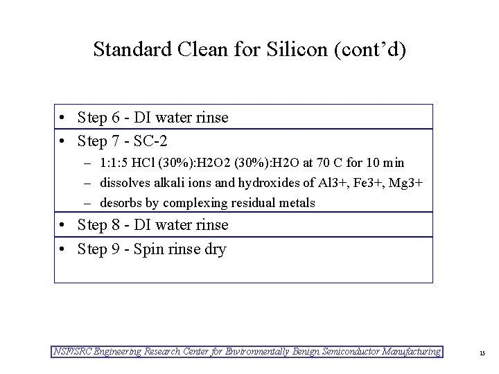
Standard Clean for Silicon (cont’d) • Step 6 - DI water rinse • Step 7 - SC-2 – 1: 1: 5 HCl (30%): H 2 O 2 (30%): H 2 O at 70 C for 10 min – dissolves alkali ions and hydroxides of Al 3+, Fe 3+, Mg 3+ – desorbs by complexing residual metals • Step 8 - DI water rinse • Step 9 - Spin rinse dry NSF/SRC Engineering Research Center for Environmentally Benign Semiconductor Manufacturing 15

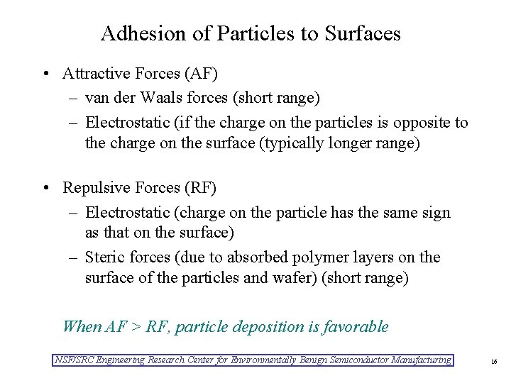
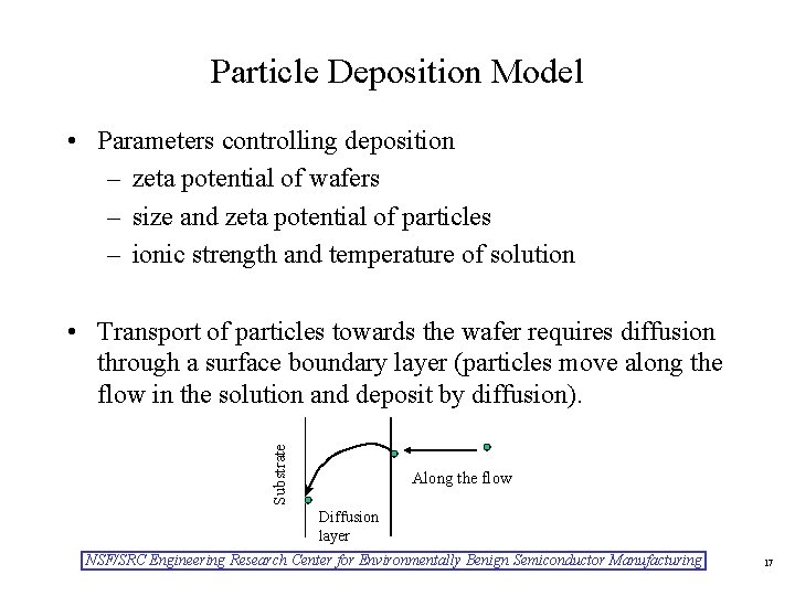
Adhesion of Particles to Surfaces • Attractive Forces (AF) – van der Waals forces (short range) – Electrostatic (if the charge on the particles is opposite to the charge on the surface (typically longer range) • Repulsive Forces (RF) – Electrostatic (charge on the particle has the same sign as that on the surface) – Steric forces (due to absorbed polymer layers on the surface of the particles and wafer) (short range) When AF > RF, particle deposition is favorable NSF/SRC Engineering Research Center for Environmentally Benign Semiconductor Manufacturing 16

Particle Deposition Model • Parameters controlling deposition – zeta potential of wafers – size and zeta potential of particles – ionic strength and temperature of solution Substrate • Transport of particles towards the wafer requires diffusion through a surface boundary layer (particles move along the flow in the solution and deposit by diffusion). Along the flow Diffusion layer NSF/SRC Engineering Research Center for Environmentally Benign Semiconductor Manufacturing 17

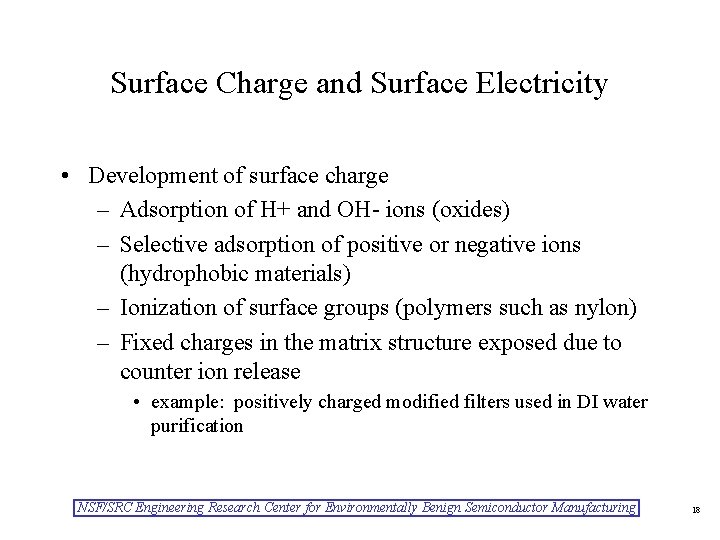
Surface Charge and Surface Electricity • Development of surface charge – Adsorption of H+ and OH- ions (oxides) – Selective adsorption of positive or negative ions (hydrophobic materials) – Ionization of surface groups (polymers such as nylon) – Fixed charges in the matrix structure exposed due to counter ion release • example: positively charged modified filters used in DI water purification NSF/SRC Engineering Research Center for Environmentally Benign Semiconductor Manufacturing 18

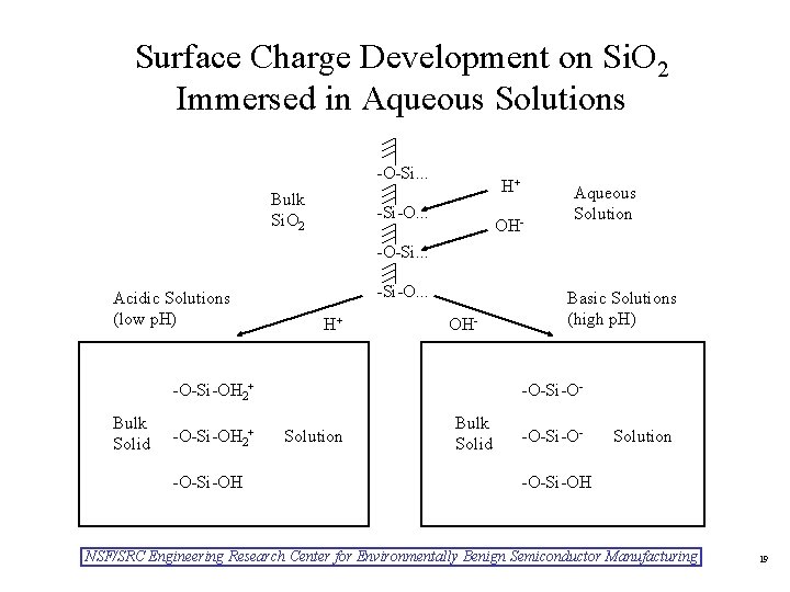
Surface Charge Development on Si. O 2 Immersed in Aqueous Solutions -O-Si. . . Bulk Si. O 2 H+ -Si-O. . . OH- Aqueous Solution -O-Si. . . Acidic Solutions (low p. H) -Si-O. . . H+ OH- -O-Si-OH 2+ Bulk Solid -O-Si-OH 2+ -O-Si-OH Basic Solutions (high p. H) -O-Si-OSolution Bulk Solid -O-Si-O- Solution -O-Si-OH NSF/SRC Engineering Research Center for Environmentally Benign Semiconductor Manufacturing 19

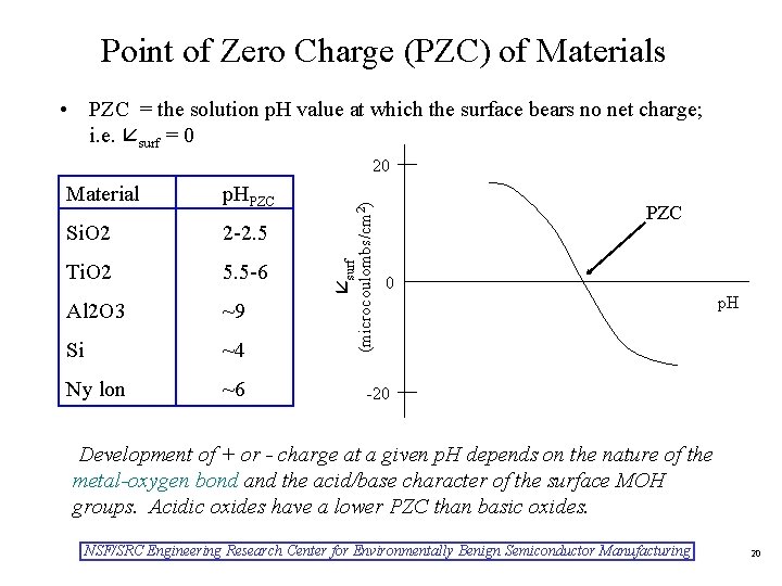
Point of Zero Charge (PZC) of Materials • PZC = the solution p. H value at which the surface bears no net charge; i. e. surf = 0 p. HPZC Si. O 2 2 -2. 5 Ti. O 2 5. 5 -6 Al 2 O 3 ~9 Si ~4 Ny lon ~6 surf Material (microcoulombs/cm 2) 20 PZC 0 p. H -20 Development of + or - charge at a given p. H depends on the nature of the metal-oxygen bond and the acid/base character of the surface MOH groups. Acidic oxides have a lower PZC than basic oxides. NSF/SRC Engineering Research Center for Environmentally Benign Semiconductor Manufacturing 20

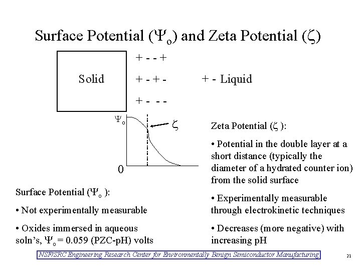
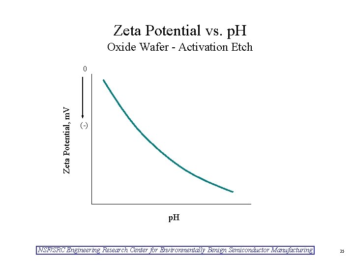
Surface Potential ( o) and Zeta Potential ( ) +--+ Solid + - Liquid +-++- - o 0 Surface Potential ( o ): Zeta Potential ( ): • Potential in the double layer at a short distance (typically the diameter of a hydrated counter ion) from the solid surface • Not experimentally measurable • Experimentally measurable through electrokinetic techniques • Oxides immersed in aqueous soln’s, o = 0. 059 (PZC-p. H) volts • Decreases (more negative) with increasing p. H NSF/SRC Engineering Research Center for Environmentally Benign Semiconductor Manufacturing 21

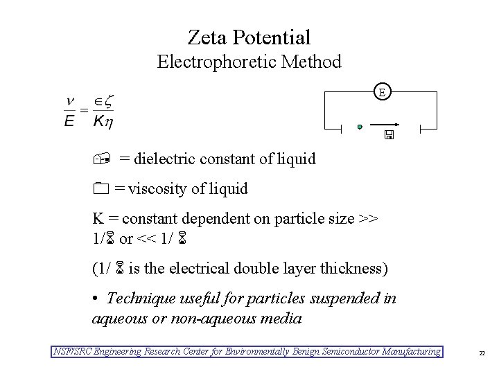
Zeta Potential Electrophoretic Method E = dielectric constant of liquid = viscosity of liquid K = constant dependent on particle size >> 1/ or << 1/ (1/ is the electrical double layer thickness) • Technique useful for particles suspended in aqueous or non-aqueous media NSF/SRC Engineering Research Center for Environmentally Benign Semiconductor Manufacturing 22

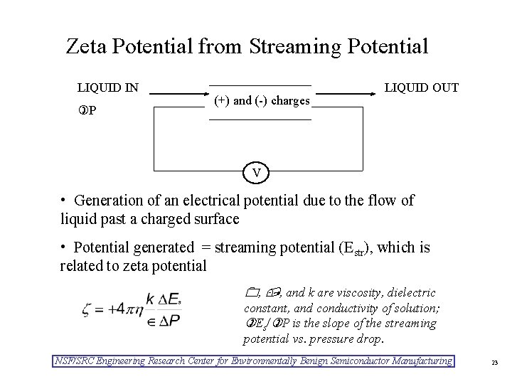
Zeta Potential from Streaming Potential LIQUID IN P (+) and (-) charges LIQUID OUT V • Generation of an electrical potential due to the flow of liquid past a charged surface • Potential generated = streaming potential (Estr), which is related to zeta potential , , and k are viscosity, dielectric constant, and conductivity of solution; Es/ P is the slope of the streaming potential vs. pressure drop. NSF/SRC Engineering Research Center for Environmentally Benign Semiconductor Manufacturing 23

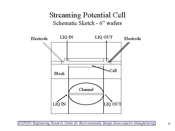
Streaming Potential Cell Schematic Sketch - 6” wafers Electrode LIQ IN LIQ OUT Electrode Cell Block Channel LIQ IN LIQ OUT NSF/SRC Engineering Research Center for Environmentally Benign Semiconductor Manufacturing 24

Zeta Potential vs. p. H Oxide Wafer - Activation Etch Zeta Potential, m. V 0 (-) p. H NSF/SRC Engineering Research Center for Environmentally Benign Semiconductor Manufacturing 25

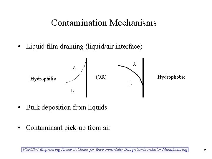
Contamination Mechanisms • Liquid film draining (liquid/air interface) A A (OR) Hydrophilic Hydrophobic L L • Bulk deposition from liquids • Contaminant pick-up from air NSF/SRC Engineering Research Center for Environmentally Benign Semiconductor Manufacturing 26