Welcome To All The Teachers of SMIT 555



- Slides: 29

Welcome To All The Teacher’s of SMIT.

555 Timer as Monostable Multivibrator. Group no. A 8 Members: v. Sourav Dhar. (071680103001) v. Sudip Kumar Pal(071680103013) v. Debayan Chakraborty(071680103019) v. Debasish Kumar Bit(071680103033)

Overview: In this presentation we are going to discuss these topics Ø Introduction of 555 Timer. Ø Different Application’s of 555 Timer. Ø 555 Timer IC pin configuration. Ø Pin details. Ø Internal Architectural Detail of 555 Timer IC. Ø Types of 555 Timer Circuit’s. Ø Operation of 555 Timer IC as Monostable Multivibrator. Ø Graphical Representation. Ø Mathematical Calculation.

Introduction To The 555 Timer v. The 555 Timer is one of the most popular and versatile integrated circuits ever produced! v. It was first introduced by Hans R. Camenzind in 1970 and brought to market in 1971 by Signetics (later acquired by Philips). v. It is 30 years old and still being used! v. It is a combination of digital and analog circuits.

v. It has been claimed that the 555 gets its name from the three 5 kΩ resistors used in typical early implementations. v. Typically it has 8 pins, but it has various versions. v. Ultra-low power versions of the 555 are also available. v It is known as the “time machine” as it performs a wide variety of timing tasks. v. Variant IC’s available include the 556 (a 14 -pin DIP combining two 555 s on one chip), and the 558 (a 16 pin DIP combining four slightly modified 555 s.

Application’s for the 555 Timer include: v. Bounce-free switches and Cascaded timers. v. Frequency dividers. v. Voltage-controlled oscillators. v. Pulse generators and LED flashers. v. Sawtooth (linear ramp) generator. v. Pulse width modulator. v. Pulse position modulator. v. Frequency divider.

v. Missing pulse detector. v. Metronome. v. Bicycle light. v. Sweeping frequency siren. v. Voltage inverter. v. Voltage doubler. v. Running/rotating light generator. v. Infrared remote control. v. Frequency to voltage converter. v. Power alarm. v. Dark detector.

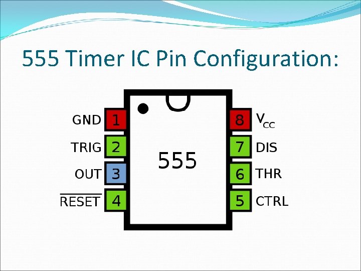
555 Timer IC Pin Configuration:

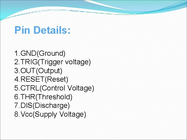
Pin Details: 1. GND(Ground) 2. TRIG(Trigger voltage) 3. OUT(Output) 4. RESET(Reset) 5. CTRL(Control Voltage) 6. THR(Threshold) 7. DIS(Discharge) 8. Vcc(Supply Voltage)

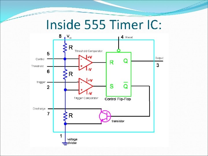
Inside 555 Timer IC:

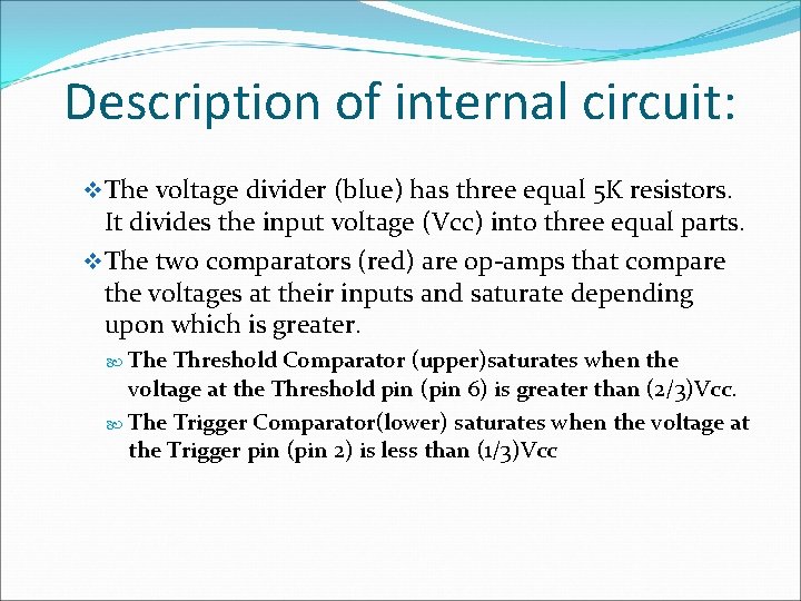
Description of internal circuit: v The voltage divider (blue) has three equal 5 K resistors. It divides the input voltage (Vcc) into three equal parts. v The two comparators (red) are op-amps that compare the voltages at their inputs and saturate depending upon which is greater. The Threshold Comparator (upper)saturates when the voltage at the Threshold pin (pin 6) is greater than (2/3)Vcc. The Trigger Comparator(lower) saturates when the voltage at the Trigger pin (pin 2) is less than (1/3)Vcc

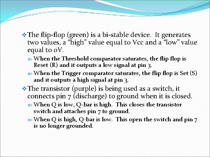
v The flip-flop (green) is a bi-stable device. It generates two values, a “high” value equal to Vcc and a “low” value equal to 0 V. When the Threshold comparator saturates, the flip flop is Reset (R) and it outputs a low signal at pin 3. When the Trigger comparator saturates, the flip flop is Set (S) and it outputs a high signal at pin 3. v The transistor (purple) is being used as a switch, it connects pin 7 (discharge) to ground when it is closed. When Q is low, Q-bar is high. This closes the transistor switch and attaches pin 7 to ground. When Q is high, Q-bar is low. This open the switch and pin 7 is no longer grounded.

Types of 555 -Timer circuits: v. There are three types of 555 -Timer circuits: - • Monostable Multivibrator. • Astable Multivibrator. • Bistable Multivibrator.

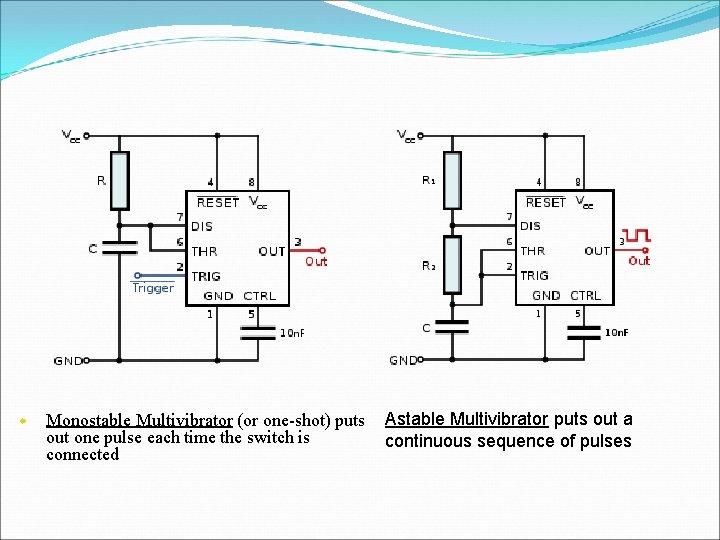
w Monostable Multivibrator (or one-shot) puts out one pulse each time the switch is connected Astable Multivibrator puts out a continuous sequence of pulses

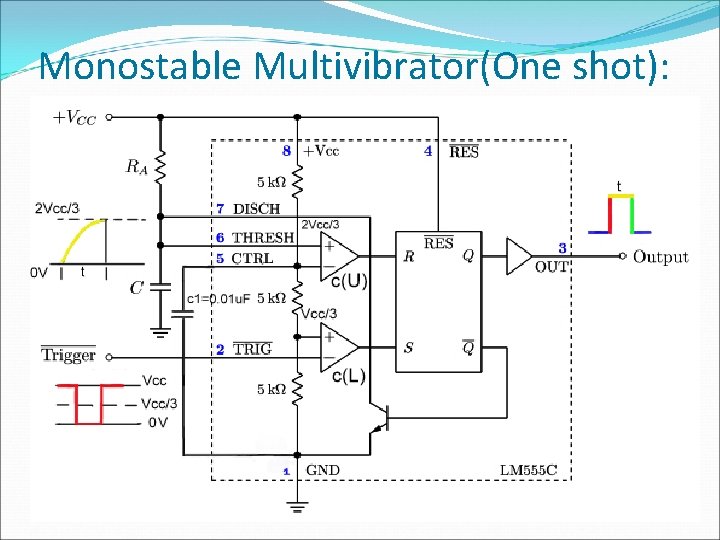
Monostable Multivibrator(One shot):

Circuit: 1. In the diagram you can see that we have connected a resistor “Ra” between the Supply Voltage(Pin 8) and Threshold Voltage (Pin 6). Also Threshold And Discharge (Pin 7) is shorted. 2. A capacitor of capacitance “C” is connected between Threshold (Pin 6) and Ground. the function of this capacitor is to suppress noise and deliver energy during the transition time of the output. 3. Between Control Voltage (Pin 5) and Ground (Pin 1) a Capacitor of capacitance 0. 01 u. F is connected.

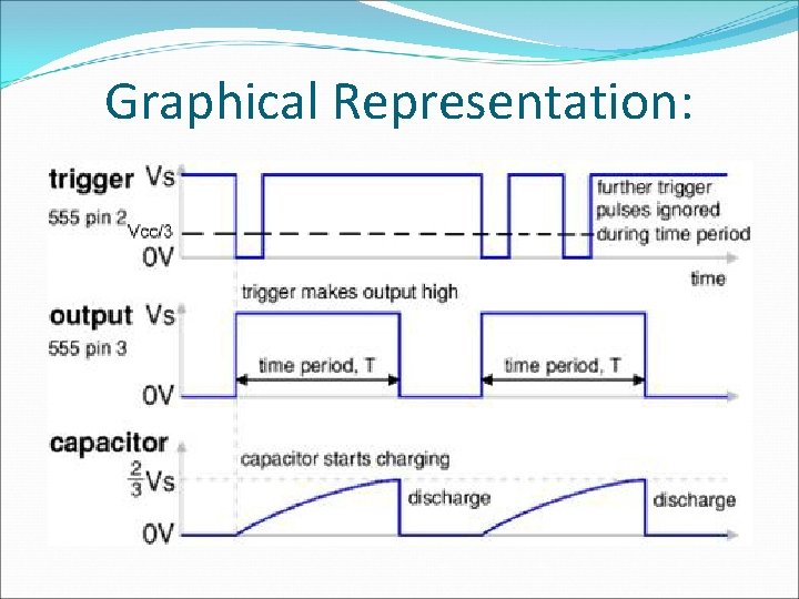
Operation: 1) We know that if we leave a capacitor alone then the capacitor will discharge gradually, so initially we can consider the voltage of capacitor “C” as 0 Volt. 2) Now to start the sequence of ----- we apply a negative trigger voltage shown in red color in left side. 3) When the trigger voltage goes below Vcc/3 voltage level, at that time in the lower comparator c(L) +ve pin voltage becomes > -ve pin voltage,

as +ve pin is fixed with Vcc/3 in 555 resistor network and –ve is connected with trigger voltage. So the output of the comparator c(L) become high. 4) Now you can see that the output of the comparator c(L) is connected with the “S” terminal of SR Flip Flop. So we know that if we give S=1 and R=0 in SR Flip Flop the out put becomes Q=1 and Q-bar=0, which starts the output signal (connected with Q) portion shown in red and it becomes high as shown in the out put graph at right side of the picture. 5) At the same time the capacitor “C” starts to become charged through resistor “Ra” from.

Vcc(shown in the upper left side of the picture), and continues upto voltage level 2 Vcc/3. 5) Suppose the capacitor takes time “t” to reach the voltage level 2 Vcc/3, so the output remains high during this time period “t” shown in “yellow” at output. And during this period any trigger voltage applied in the trigger pin will have no effect on the output. 6) Now the capacitor Reaches to voltage level 2 Vcc/3 and exceeds the voltage, at that time in the comparator c(U) the +ve pin voltage becomes > the –ve voltage level, as +ve pin is connected with capacitor and –ve pin is fixed

Level in 555 resistor network. 7) Here you can see that the R pin in SR flip flop is connected with the output of the comparator c(U). So the input of SR flip flop is S=0 and R=1 and output is Q=0 and Q-bar=1. 8) As shown in picture Q ia connected with the output so, output becomes low shown in green color in output graph. 9) Again we can see that Q-bar is connected with the gate of the discharge BJT, whose collector is connected with the capacitor “C” and emitter is grounded. So if the Gate voltage is “ 1” then the gate opens and the capacitor discharges

through the capacitor and becomes o. V as it was initially, shown in capacitor charactaristics graph. 10) Now the whole circuit is in the stage as it was initially. Now if we give another trigger pulse at trigger pin the whole sequence starts again. By this way the 555 Timer works as monostable multivibrator in which we get a regulated time output pulse for each trigger voltage.

Graphical Representation:

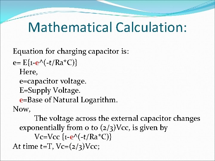
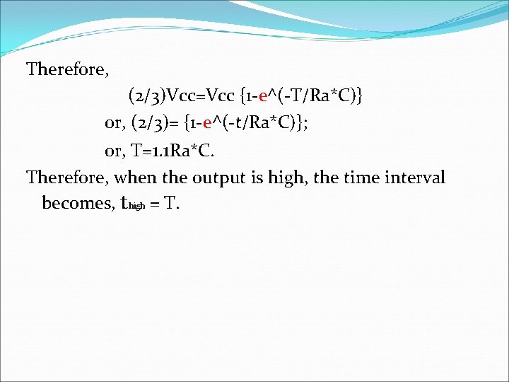
Mathematical Calculation: Equation for charging capacitor is: e= E{1 -e^(-t/Ra*C)} Here, e=capacitor voltage. E=Supply Voltage. e=Base of Natural Logarithm. Now, The voltage across the external capacitor changes exponentially from 0 to (2/3)Vcc, is given by Vc=Vcc {1 -e^(-t/Ra*C)} At time t=T, Vc=(2/3)Vcc;

Therefore, (2/3)Vcc=Vcc {1 -e^(-T/Ra*C)} or, (2/3)= {1 -e^(-t/Ra*C)}; or, T=1. 1 Ra*C. Therefore, when the output is high, the time interval becomes, thigh = T.

Practical Circuits: Some of the frequently used practical circuits are. § Linear Ramp Generator. § Missing Pulse Detector. § Pulse Width Modulator. § Frequency Divider. § Ten Minute Timer.

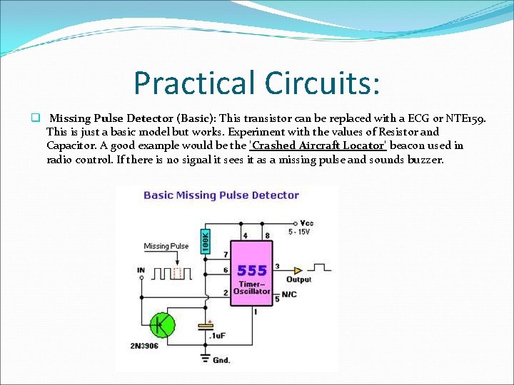
Practical Circuits: q Missing Pulse Detector (Basic): This transistor can be replaced with a ECG or NTE 159. This is just a basic model but works. Experiment with the values of Resistor and Capacitor. A good example would be the 'Crashed Aircraft Locator' beacon used in radio control. If there is no signal it sees it as a missing pulse and sounds buzzer.

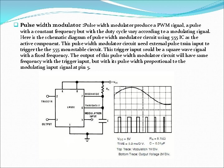
q Pulse width modulator : Pulse width modulator produce a PWM signal, a pulse with a constant frequency but with the duty cycle vary according to a modulating signal. Here is the schematic diagram of pulse width modulator circuit using 555 IC as the active component. This pulse width modulator circuit need external pulse train input to trigger the 555 monostable circuit. This trigger input sould be a square wave signal with a fixed frequency. The output of this pulse width modulator circuit will have same frequency with the trigger input, but with its pulse width proportional to the modulating input signal at pin 5.

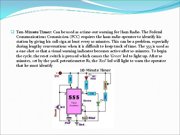
q Ten-Minute Timer: Can be used as a time-out warning for Ham Radio. The Federal Communications Commission (FCC) requires the ham radio operator to identify his station by giving his call-sign at least every 10 minutes. This can be a problem, especially during lengthy conversations when it is difficult to keep track of time. The 555 is used as a one-shot so that a visual warning indicator becomes active after 10 -minutes. To begin the cycle, the reset switch is pressed which causes the 'Green' led to light up. After 10 minutes, set by the 500 K potentiometer R 1, the 'Red' led will light to warn the operator that he must identify

THANK YOU