Week 6 Chapter 3 FET SmallSignal Analysis Mohd

 to ID (output) is called")


 Configuration In a CD amplifier configuration the input is on")


![Impedances Input Impedance: 9. 52] [Formula Output Impedance: 9. 53] [Formula](https://slidetodoc.com/presentation_image_h/1178cf118ab661048460a94c02d014bc/image-68.jpg "Impedances Input Impedance: 9. 52] [Formula Output Impedance: 9. 53] [Formula")
![Voltage Gain [Formula 9. 55] [Formula 9. 56]](https://slidetodoc.com/presentation_image_h/1178cf118ab661048460a94c02d014bc/image-69.jpg "Voltage Gain [Formula 9. 55] [Formula 9. 56]")


- Slides: 80
Week 6 – Chapter 3 FET Small-Signal Analysis Mohd Shawal Jadin FKEE UMP © 2009
FET Small-Signal Model Transconductance The relationship of VGS (input) to ID (output) is called transconductance. The transconductance is denoted gm. Transfer Curve
Graphical Determination of gm
Mathematical Definition of gm Using differential calculus
FET Impedance Input Impedance Zi: • Very large to assume input terminal approximate an open circuit Output Impedance Zo: yos: admittance equivalent circuit parameter listed on FET specification sheets.
FET Specification
FET AC Equivalent Circuit
JFET Fixed-Bias Configuration The input is on the gate and the output is on the drain.
JFET Fixed-Bias Configuration Once again: same step as BJT to redraw the network to AC equivalent circuit. Capacitor – short circuit DC batteries VGG and VDD are set to zero volts by a short-circuit equivalent
AC Equivalent Circuit
AC Equivalent Circuit
Impedances Input Impedance: Output Impedance:
Voltage Gain
Phase Relationship A CS amplifier configuration has a 180 -degree phase shift between input and output.
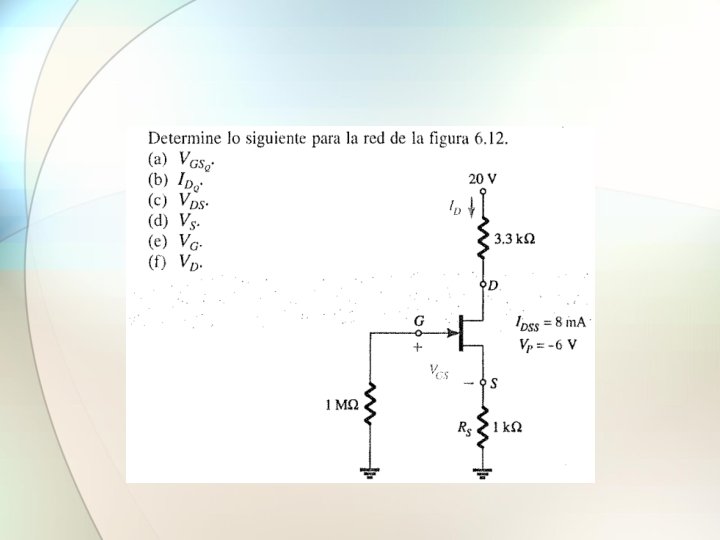
Example Fixed-bias configuration has an operating point defined by VGSQ = -2 V and IDQ = 5. 625 m. A, with IDSS = 10 m. A and VP = -8 V. The value of yos is provided as 40 µS. Determine: a) gm b) Zi c) Zo d) AV e) AV ignoring the effects of rd
Solution
JFET CS Self-Bias Configuration This is a CS amplifier configuration therefore the input is on the gate and the output is on the drain.
AC Equivalent Circuit
Impedances Input Impedance: Output Impedance:
Voltage Gain
Phase Relationship A CS amplifier configuration has a 180 -degree phase shift between input and output.
JFET CS Self-Bias Configuration – Unbypassed Rs If Cs is removed, it affects the gain of the circuit.
AC Equivalent Circuit
Impedances Input Impedance: Output Impedance:
Impedances
Voltage Gain
Voltage Gain
Example
Solution
Solution
JFET CS Voltage-Divider Configuration This is a CS amplifier configuration therefore the input is on the gate and the output is on the drain.
AC Equivalent Circuit
Impedances Input Impedance: Output Impedance:
Voltage Gain
JFET Source Follower (Common-Drain) Configuration In a CD amplifier configuration the input is on the gate, but the output is from the source.
AC Equivalent Circuit
Impedances Input Impedance: Output Impedance:
Voltage Gain
Phase Relationship A CD amplifier configuration has no phase shift between input and output.
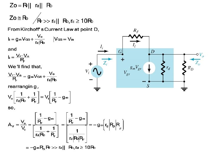
JFET Common-Gate Configuration The input is on source and the output is on the drain.
AC Equivalent Circuit
Impedances Applying Kirchhoff’s voltage law around the output perimeter and Kirchhoff’s current law at node a : :
Impedances Input Impedance: Output Impedance:
Voltage Gain Applying Kirchhoff’s current law at node b : :
Phase Relationship A CG amplifier configuration has no phase shift between input and output.
Depletion-Type MOSFETs 1. D-MOSFETs have similar AC equivalent models. 2. The only difference is that VSGQ can be positive for nchannel devices and negative for p-channel devices. 3. This means that gm can be greater than gm 0.
D-MOSFET AC Equivalent Model
• Find Example – VGSQ and IDQ – Determine gm and compare to gm 0 – rd – Find Zi, Zo, Av
Enhancement-Type MOSFETs There are two types of E-MOSFETs: n. MOS or n-channel MOSFETs p. MOS or p-channel MOSFETs
E-MOSFET AC Equivalent Model Forward transfer admittance gm and rd can be found in the specification sheet for the FET.
E-MOSFET CS Drain-Feedback Configuration
AC Equivalent Circuit
Impedances Input Impedance: Output Impedance:
The calculation
The AC analysis of E-MOSFET Remember that, the biasing arrangement are limited for E-MOSFET
Voltage Gain
Phase Relationship This is a CS amplifier configuration therefore it has 180 -degree phase shift between input and output.
Do it • Determine input and output and also AV impedance for k=0. 3 X 10 -3
E-MOSFET CS Voltage-Divider Configuration
AC Equivalent Circuit
Impedances Input Impedance: Output Impedance:
Voltage Gain
Phase Relationship This is a CS amplifier configuration therefore it has 180 -degree phase shift between input and output.
Solution
E-MOSFET CS Voltage-Divider Configuration
AC Equivalent Circuit
Impedances Input Impedance: 9. 52] [Formula Output Impedance: 9. 53] [Formula
Voltage Gain [Formula 9. 55] [Formula 9. 56]
Summary Table
Summary Table
Try yourself • Design a self-bias network that have gain of 10. The device should be biased at VGSQ=1/3 VP
Solution