Wafer Preparation Challenge in epitaxial growth Achieving defect


Removing the organic and metallic impurities from")


 is")


 Surface reaction limited Nonthermal equil.")


")
 150 nm")


 The film")


 Dcs(Si. H 2 Cl 2 )is the only one that has been applied")

- Slides: 43
Wafer Preparation Challenge in epitaxial growth : - Achieving defect free films at low temperate. l More than half of the yield loss is due to contamination such as organic and metallic impurities. ------- surface preparation is important
Wafer Preparation Surface preparation prior to epi growth generally consist of 2 part : (1) ex-situ clean : RCA cleaning (2) in-situ clean : high temperature annealing
RCA and HF dip RCA Clean : (1)Removing the organic and metallic impurities from the silicon surface by oxidizing the silicon surface (2) Forming complexes with the contaminants, which become water-soluble. .
HF dip After the RCA clean - the silicon surface is left passivated with a chemical oxide , which protect the surface against recontamination HF dip : Removing the chemical oxide and the native oxide to achieve the atomically clean silicon surface
HF clean To accomplish low temperature epitaxy, one must have an atomically clean Si surface 1. The Si surface is Si-H terminated 2. Highly resistant to oxidation HF clean 3. May be exposed to room air for several minutes without significant oxidation
After HF Dip HF : DI =1 : 85 ~1 : 200 H passivation H H H H O H H H
H 2 Prebake If the temp. of H 2 bake is higher than 1000°C ----no HF etch is necessary And ------surface is better than HF dip followed by a H 2 pre-bakes at 900°C or less.
High Temp. Effect of H 2 Prebake But high temp. may causes
Low Temp. Bake The commercial UHCVD systems that are capable of bake temperature (Epi. Gress) usually require 20 minutes at 800ºC to have an O & C free interface. but the problem is : The Epi. Gress takes a lot time to ramp up to 800ºC then cool to a deposition temperature of 550 -650ºC ------- Not too good for throughput
Low Temp. Bake ASM has developed a novel hydrogen prebake that has the potential lower the bake temperatures (below 700ºC). If this novel technique is combined with plasma NF 3 chamber cleaning at say the benefits to throughput would also be significant
Water Vapor and Bake Conditions Water vapor is the most persistent contaminate in any vacuum system The effectiveness of the bake at a given temperature is directly proportional to the water and oxygen background in a given system
Surface Oxide Formation by Moisture
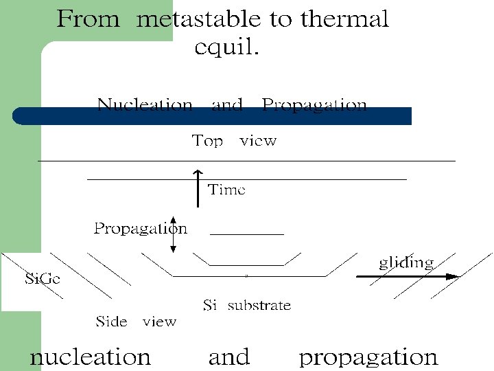
Si. Ge Epitaxial growth Choosing a Growth Temperature : - tc (critical thickness) is the most important factor - IF the critical layer thickness for a given Ge fraction is exceeded , misfit dislocation injection occurs.
Critical Thickness
Metastable state
Metastable state l Growth conditions At low Temp. (625ºC) Surface reaction limited Nonthermal equil. l Fewer dislocations than expected , when t>tc
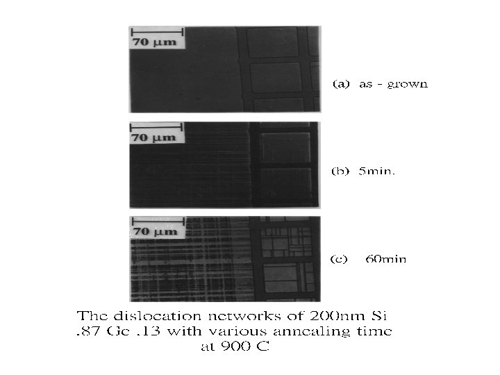
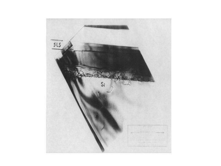
Misfit dislocation The thickness of Si. Ge growth >tc The film relaxs Misfit dislocation l This relaxation is catastrophic for Si. Ge HBT application
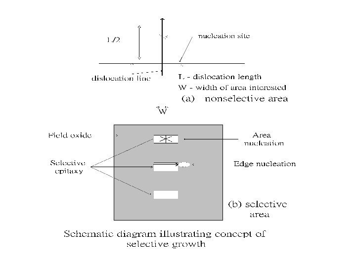
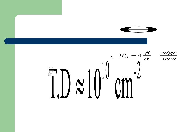
Dislocation number The number of dislocation in non-selective area
Dislocation number The number of dislocation in the selective area
Enhancement Factor (EF)
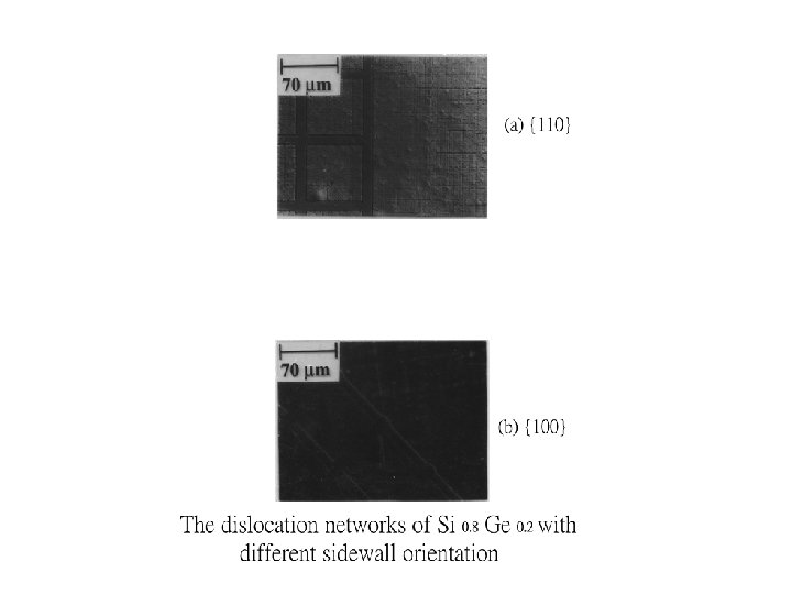
Si 0. 8 Ge 0. 2 l Two samples were studied (A) 150 nm with hole edge aligned with {100} direction (B) 200 nm with hole edge aligned with {100} direction
Si 0. 8 Ge 0. 2 {110} {100}
Threading dislocation in HBT
Threading dislocation
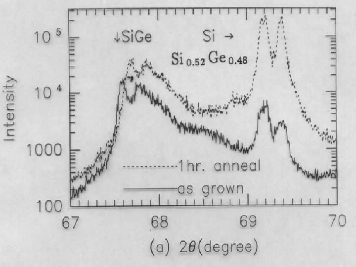
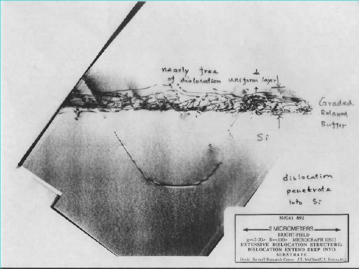
Gradual relaxed buffer
Strain after anneal
Deposition temperature Once this critical thickness guideline is satisfied : Deposition temperature(T) The film quality for the epitaxial film
Film Quality when T decrease, the silane flow must decrease also. ex: T : 700ºC ; 100% silane : 50 sccm------will deposit a specular high quality film. but T : 600°C ; 100% silane : 50 sccm-----the film beome hazy
Film Quality Faceting/Conformality - Lower temperature and the resultant lower growth rates result in less faceting and improved conformality l Poly/Si growth ratio - Low T favors epi growth - High T favors poly growth
Dichlorosilane(DCS) Dcs(Si. H 2 Cl 2 )is the only one that has been applied to the growth of Si. Ge epitaxial layers - Si. Cl 2 on the surface is then thought to react with hydrogen to form HCL and a silicon adatom
Advantage of DCS over silane Specular defect free surface -----Superior surfaces are evident with DCS even when processing at extremely low temperatures as a result of the HCL released in the decomposition Safety -----silane is explosive and highly pyrophoric