Wafer bonding Chapter 17 CMP Chapter 16 sami
 & CMP (Chapter 16) sami. franssila@aalto. fi")
Wafer bonding (Chapter 17) & CMP (Chapter 16) sami. franssila@aalto. fi
 – Packaging – Capping/Encapsulation – Multi layer")
Wafer bonding applications – Advanced substrates (SOI) – Packaging – Capping/Encapsulation – Multi layer devices – 3 D structures – Layer transfer Wire bonding Flip chip bonding Not part of this course

Wafer bonding techniques • direct bonding: Si/Si, glass/glass, PMMA/PMMA, … also known as fusion bonding • anodic bonding (AB): Si/glass, glass/Si/glass • thermo-compression bonding (TCB): Au-Au • eutectic bonding: Si/Au (363 o. C) • glass frit bonding: glass melting • adhesive bonding: “glues” applied, any substrate
 Wafer are smooth")
Basic requirements for bonding Wafers are flat (no centimeter scale wavyness) Wafer are smooth (atomic/micrometer scale) Materials form chemical bonds across their interface High stresses are avoided No interface bubbles develop
 vacuum pumping -(optional) wafer alignment")
Bonding process steps -particle removal -surface chemistry modification -(optional) vacuum pumping -(optional) wafer alignment -room temperature joining -application of force/heat/voltage -(optional) wafer thinning

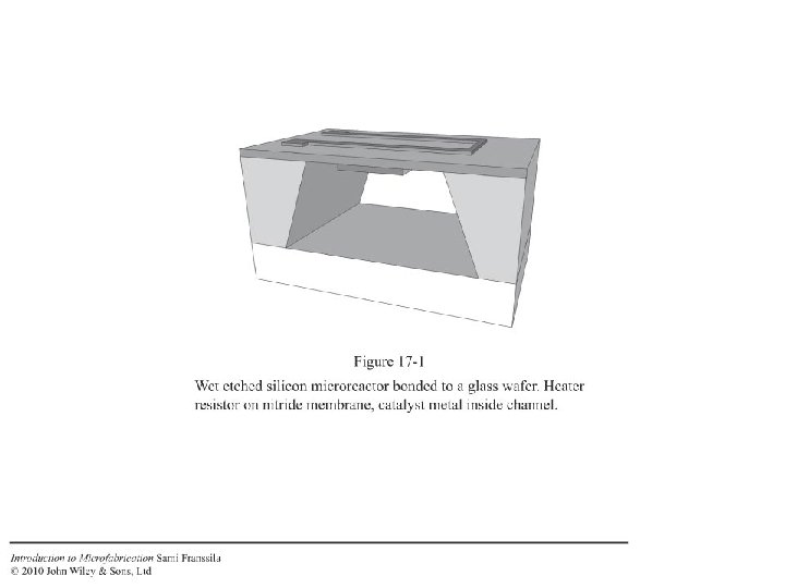
SOI wafer fabrication: bonding an oxidized wafer to a bare silicon wafer device Si BOX Handle Si a) surface preparation b) room temperature joining c) annealing for bond improvement d) top wafer thinning BOX= buried oxide

Bond strength Tong & Gösele: Semiconductor wafer bonding

Silicon bonding At low temperature: At high temperature: weak hydrogen bonds strong Si-O-Si bonds Tong & Gösele: Semiconductor wafer bonding

Why SOI wafers ? CMOS MEMS -easy isolation of transistors -fewer process steps -elimination of substrate effects faster transistors -easy etch stop -single crystal material superior -device and handle silicon optimized separately Why not SOI ? Expensive
 SOI wafer Processed bulk wafer")
Silicon fusion bonding: c. MUT (capacitive micromachined ultrasonic transducer) SOI wafer Processed bulk wafer Etching away SOI handle and BOX Processing electrodes on the device SOI membrane Yongli Huang, JMEMS 2003, p. 128
 – Same cleaning, particle, surface chemistry problems as")
Glass-to-glass fusion bonding (Ville Saarela, unpublished) – Same cleaning, particle, surface chemistry problems as in Si-Si fusion bonding – Wafer stack is heated close to glass “softening temperature” (e. g. 650 °C for Pyrex 7740) – Deformation due to glass flux Isotropically wet etched channel in glass with fusion bonded glass channel. 12

Polymer fusion bonding Wafers are heated above glass transition temperature Tg and pressed together. Tg usually 100 -200 o. C Works best for two identical wafers. Also called thermal bonding

Anodic bonding: Si-glass At elevated temperature Na+ ions in glass become mobile Electric field drives Na+ towards cathode Oxygen O- ions in glass migrate towards silicon anode Depletion region High electric field Attraction of wafers

Anodic bonding: Si-glass Double Sided Heating: e. g. 350°C High Voltage: e. g. 500 V Bonding Atmosphere: e. g. 1 mbar nitrogen

Thermal matching Si-glass • Coefficients of thermal expansion of silicon and glass must be matching, otherwise cracking upon cooling only certain glasses suitable for anodic bonding: Pyrex, Borofloat

Anodic bonding: capacitor Silicon DRIE etched Al capacitor electrode Al counter electrode on a glass wafer • Materials must tolerate ca. 400 o. C • Accurate gap control because no intermediate materials

Glass-silicon-glass anodic bonding Fig. 1. 10: Oxyhydrogen burner of a flame ionization detector by Pyrexglass/silicon/Pyrex-glass bonding, from ref. Zimmermann 2002.
 • glues (e. g. silk screen printing)")
Adhesive bonding • photoresists (spin coated, photopatterned) • glues (e. g. silk screen printing) • Applicable to almost any material • If thick photoresist used, not sensitive to particles • Temperatures 100 -200 o. C (resists are polymers !)
 Because of low temperature, CMOS electronics not affected Spin coating determined")
Adhesive bonding (2) Because of low temperature, CMOS electronics not affected Spin coating determined thickness (and actuation voltage)

Bond alignment None Perfect Misaligned Simple equipment enough Requires advanced tools Some devices more sensitive to misalignment than others.
 Critical alignment Non-critical alignment")
Bond alignment (2) Critical alignment Non-critical alignment

Glass frit bonding for MEMS packaging • Glass frit is a particle slurry of low melting point glass and organic binders. • It is spread by silk screen printing (thickness e. g. 10 µm). • Cured at ca. 400 o. C (solvent evaporates and glass particles fuse together)

Comparing bonding methods
 combines chemical action with mechanical abrasion")
CMP: Chemical-Mechanical Polishing • Chemical Mechanical Polishing (CMP) combines chemical action with mechanical abrasion to achieve selective material removal through polishing Microfabrication 25

Applications of polishing Smoothing Planarization Si. O 2 Damascene Al Cu

Applications of polishing Smoothing Planarization Si. O 2 Al Damascene Cu

Applications of polishing Smoothing Planarization Si. O 2 Al Damascene Cu

Results of CMP of Si. O 2 Si. C wafer before and after CMP Microfabrication 29

Rotary CMP tool 60 -90 s per wafer

Polishing in action Polishing pad

Grinding vs. polishing 500 µm 10 µm Both use abrasive particles, but: Grinding removes 10 µm/min in large chunks because large particles Grinding results in very rough surface because very large chunks Grinding leaves mechanical damage due to large chunks being torn off Polishing uses nanoparticles to achieve smooth surfaces Polishing removes 0. 1 µm/min because small particles, small forces Mechanism is removal is chemical and mechanical (CMP !)

After grinding, need polishing Planarization Si. O 2 Damascene Al Cu

Erosion and dishing in CMP Size dependent Pattern density dependent

Photonic crystal by CMP

Log pile photonic crystal fabrication Poly-Si Si wafer CVD of oxide CMP of oxide CVD of poly-Si

Poly-Si litho & etching CVD of poly-Si CVD of oxide CMP of oxide

Etch all CVD oxide away with HF
- Slides: 38