Voltage Reference Design Considerations for a High Performance


- Slides: 17

Voltage Reference Design Considerations for a High Performance System Shailesh Khole USPAS 2017 (LLRF Class) 20 th January 2017

Introduction Selection of Voltage Reference Improvement in the performance! Component Selection & Layout How to test? 2 Shailesh Khole | Voltage Reference Design Considerations 3/11/2021

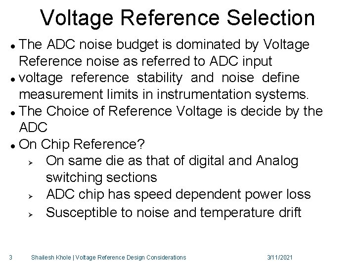
Voltage Reference Selection The ADC noise budget is dominated by Voltage Reference noise as referred to ADC input voltage reference stability and noise define measurement limits in instrumentation systems. The Choice of Reference Voltage is decide by the ADC On Chip Reference? Ø On same die as that of digital and Analog switching sections Ø ADC chip has speed dependent power loss Ø Susceptible to noise and temperature drift 3 Shailesh Khole | Voltage Reference Design Considerations 3/11/2021

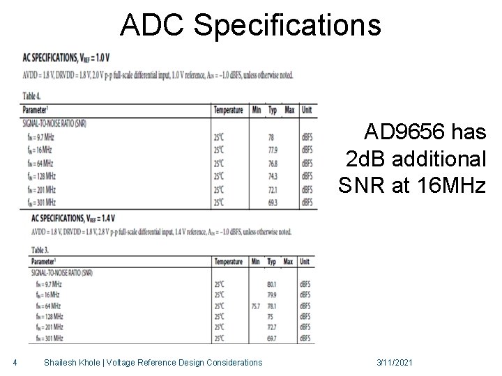
ADC Specifications AD 9656 has 2 d. B additional SNR at 16 MHz 4 Shailesh Khole | Voltage Reference Design Considerations 3/11/2021

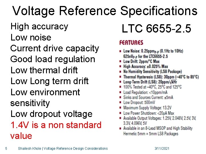
Voltage Reference Specifications High accuracy Low noise Current drive capacity Good load regulation Low thermal drift Low Long term drift Low environment sensitivity Low dropout voltage 1. 4 V is a non standard value 5 Shailesh Khole | Voltage Reference Design Considerations LTC 6655 -2. 5 3/11/2021

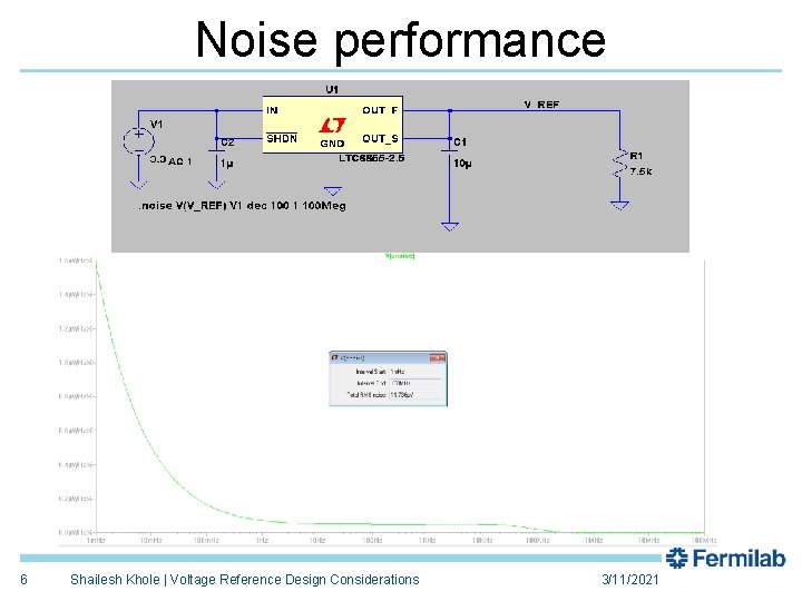
Noise performance 6 Shailesh Khole | Voltage Reference Design Considerations 3/11/2021

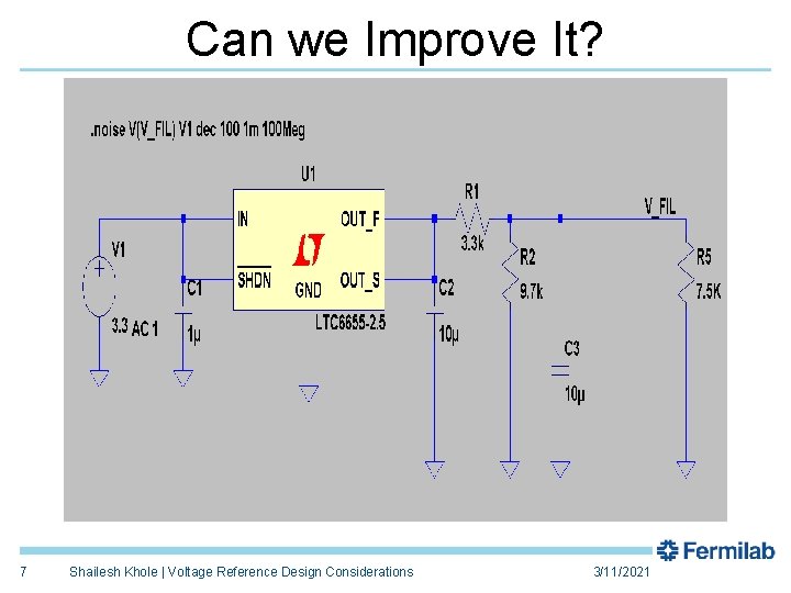
Can we Improve It? 7 Shailesh Khole | Voltage Reference Design Considerations 3/11/2021

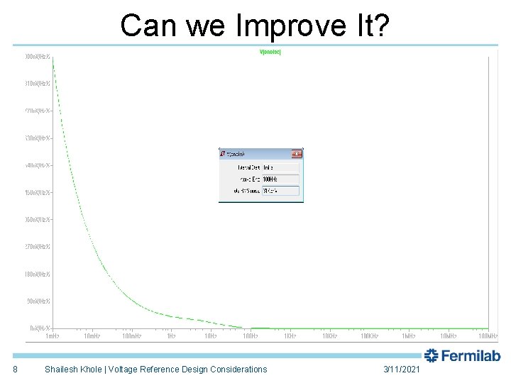
Can we Improve It? 8 Shailesh Khole | Voltage Reference Design Considerations 3/11/2021

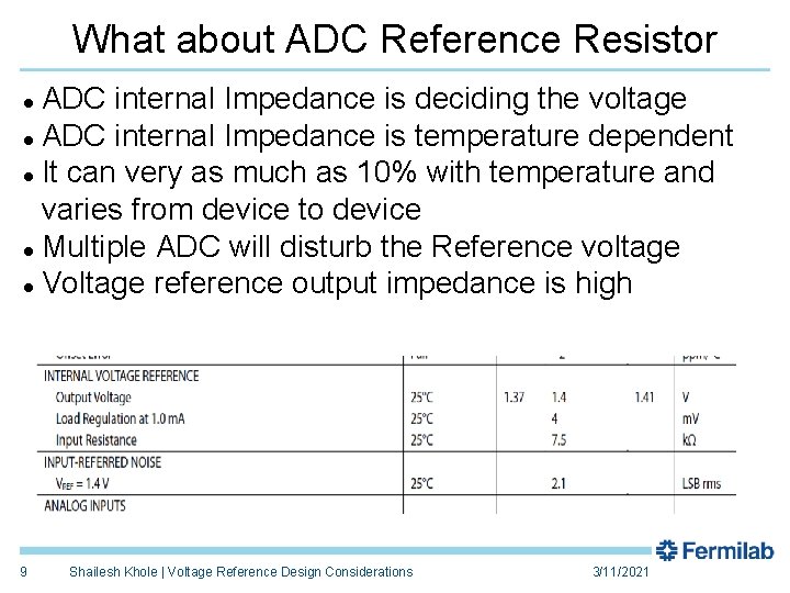
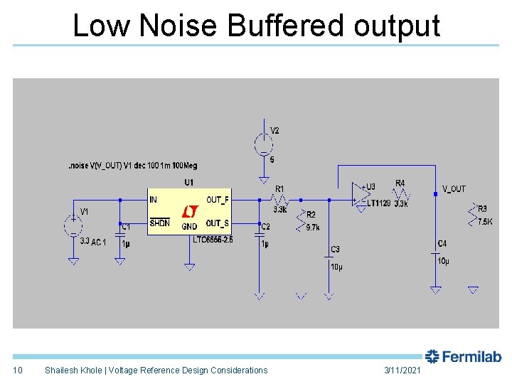
What about ADC Reference Resistor ADC internal Impedance is deciding the voltage ADC internal Impedance is temperature dependent It can very as much as 10% with temperature and varies from device to device Multiple ADC will disturb the Reference voltage Voltage reference output impedance is high 9 Shailesh Khole | Voltage Reference Design Considerations 3/11/2021

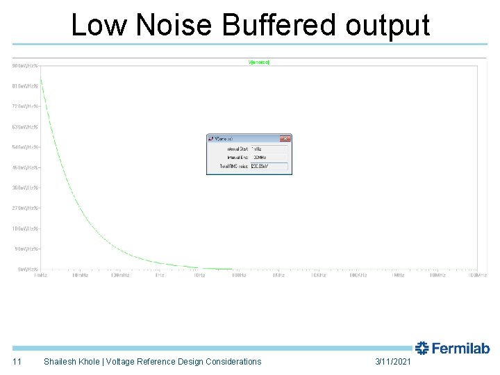
Low Noise Buffered output 10 Shailesh Khole | Voltage Reference Design Considerations 3/11/2021

Low Noise Buffered output 11 Shailesh Khole | Voltage Reference Design Considerations 3/11/2021

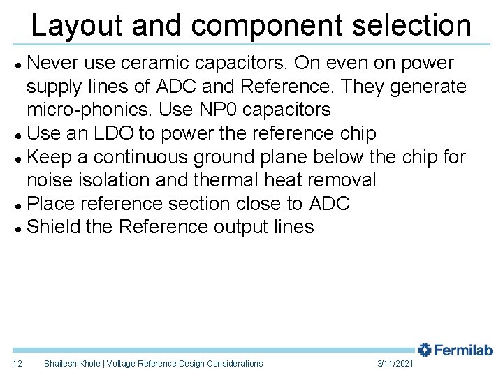
Layout and component selection Never use ceramic capacitors. On even on power supply lines of ADC and Reference. They generate micro-phonics. Use NP 0 capacitors Use an LDO to power the reference chip Keep a continuous ground plane below the chip for noise isolation and thermal heat removal Place reference section close to ADC Shield the Reference output lines 12 Shailesh Khole | Voltage Reference Design Considerations 3/11/2021

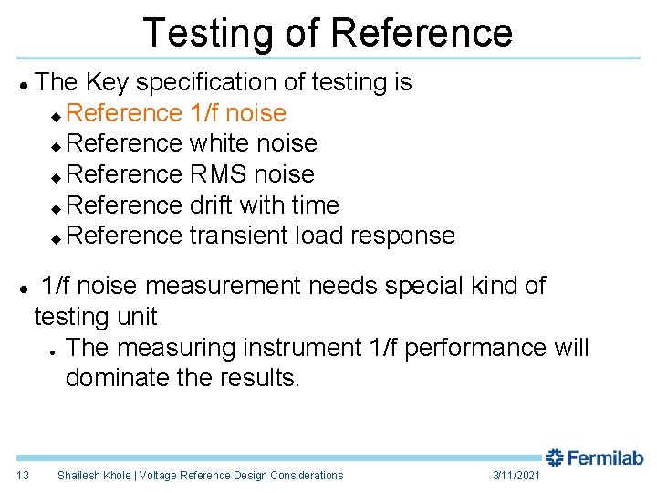
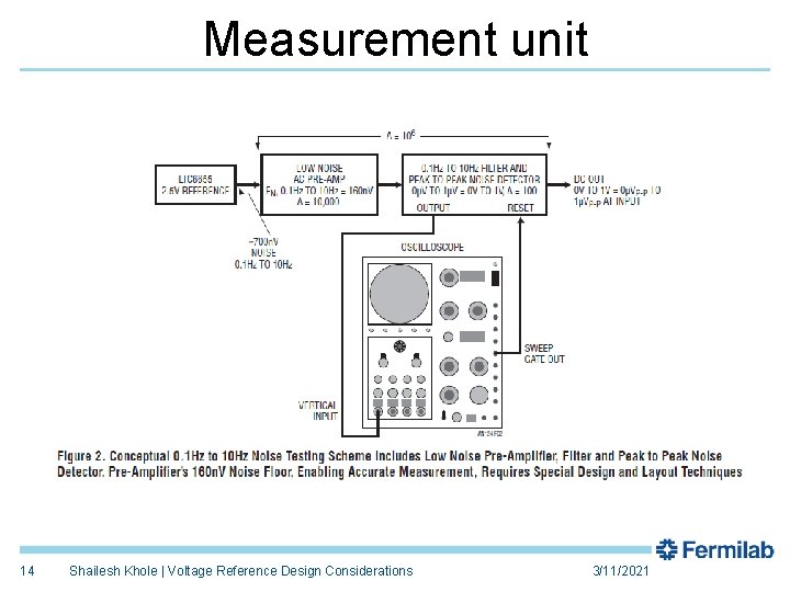
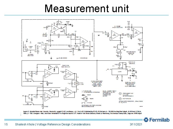
Testing of Reference 13 The Key specification of testing is Reference 1/f noise Reference white noise Reference RMS noise Reference drift with time Reference transient load response 1/f noise measurement needs special kind of testing unit The measuring instrument 1/f performance will dominate the results. Shailesh Khole | Voltage Reference Design Considerations 3/11/2021

Measurement unit 14 Shailesh Khole | Voltage Reference Design Considerations 3/11/2021

Measurement unit 15 Shailesh Khole | Voltage Reference Design Considerations 3/11/2021

References Linear Technology LT 6655 Data sheet LT 1128 Data sheet Application Note AN 124 Analog devices AD 9656 Data sheet Application Note AN 835 for ADC specification testing and performance evaluation 16 Shailesh Khole | Voltage Reference Design Considerations 3/11/2021

Thanks 17 Presenter | Presentation Title 3/11/2021