
Voltage multipliers and charge pump devices Romano Torres


- Slides: 11
Voltage multipliers and charge pump devices Romano Torres 6 th March 2013
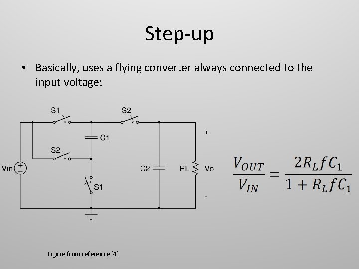
Step-up • Basically, uses a flying converter always connected to the input voltage: Figure from reference [4]
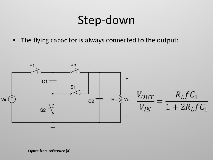
Step-down • The flying capacitor is always connected to the output: Figure from reference [4]
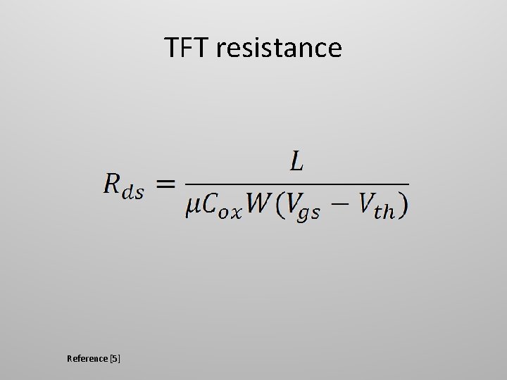
TFT resistance Reference [5]
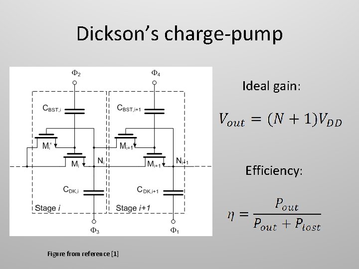
Dickson’s charge-pump Ideal gain: Efficiency: Figure from reference [1]
Voltage doubler design • Low parasitic capacitance • Low threshold voltage • Low output resistance Figure from reference [1]
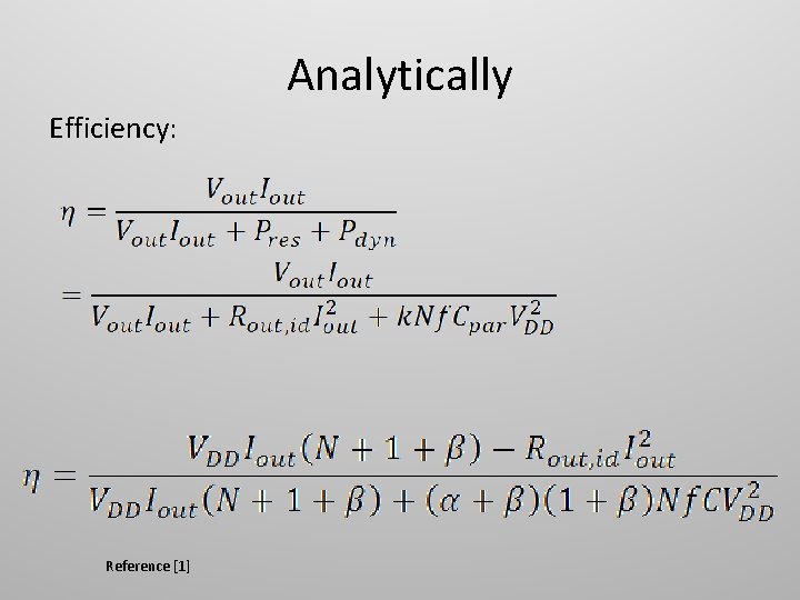
Analytically Efficiency: Reference [1]
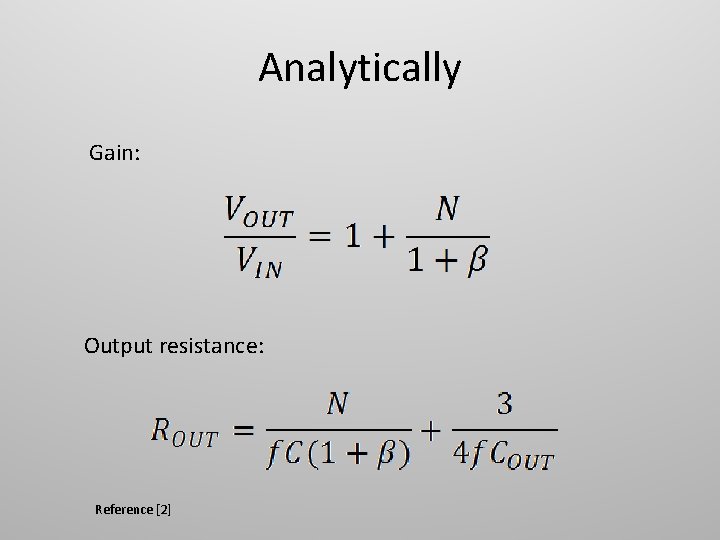
Analytically Gain: Output resistance: Reference [2]
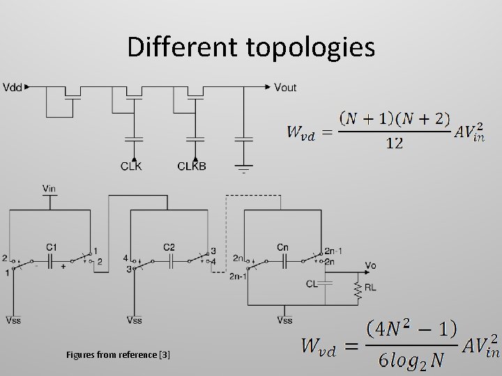
Different topologies Figures from reference [3]
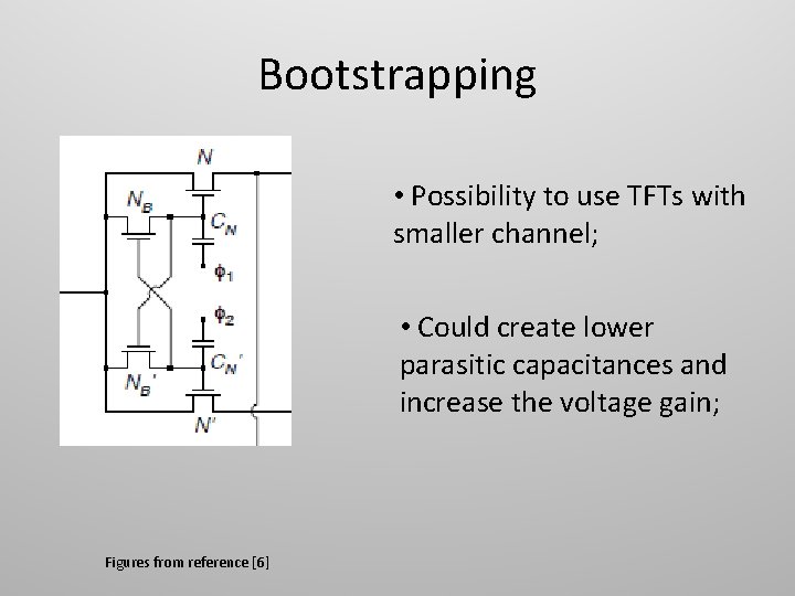
Bootstrapping • Possibility to use TFTs with smaller channel; • Could create lower parasitic capacitances and increase the voltage gain; Figures from reference [6]
References • • • [1] D. Baberna, A. Cabrini, G. Torelli and M. Pasotti, “Efficiency Comparison between Doubler and Dickson Charge Pumps, ” in Circuits and Systems IEEE International Symposium vol. 2, 2005, pp. 1891 -1894. [2] A. Cabrini, L. Gobbi and G. Torelli, “Theoretical and Experimental Analysis of Dickson Charge Pump Output Resistance, ” in Circuits and Systems IEEE International Symposium, 2006, pp. 2749 -2752. [3] J. Starzyk. “A DC-DC Charge Pump Design based on Voltage Doublers, ” in IEEE Transactions on Circuits and Systems-I: Fundamental Theory and Applications, 48: 350– 358, 2001. [4] M. Wens and M. Steyaert. Design and Implementation of Fully-Integrated Inductive DC-DC Converters in Standard CMOS. Springer, 2011. ISBN 978 -94 -007 -1435 [5] A. Saiz-Vela, P. Miribel-Català, J. Colomer, M. Puig-Vidal and J. Samitier. ”Accurate Design of Two-Phase Voltage Doublers based on a Compact Mathematical Model, ” in Circuits and Systems 5 th Midwest Symposium, 2007, pp. 213 -216. [6] Y. Allasasmeh and S. Gregori, “Switch Bootstrapping Technique for Voltage Doublers and Double Charge Pumps, ” in Circuits and Systems IEEE International Symposium, 2011, pp. 494 -497.