VLSI Testing and DFT Course Design For Testability
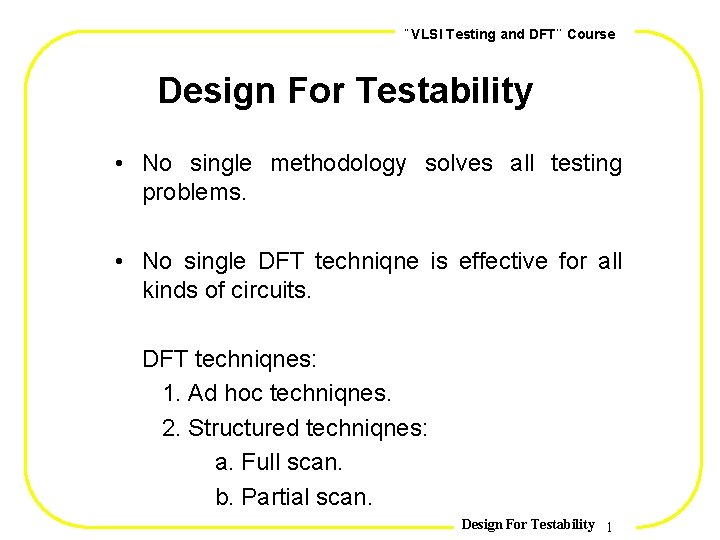
, , VLSI Testing and DFT Course Design For Testability • No single methodology solves all testing problems. • No single DFT techniqne is effective for all kinds of circuits. DFT techniqnes: 1. Ad hoc techniqnes. 2. Structured techniqnes: a. Full scan. b. Partial scan. Design For Testability 1
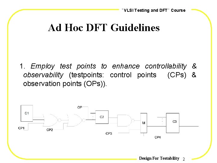
, , VLSI Testing and DFT Course Ad Hoc DFT Guidelines 1. Employ test points to enhance controllability & observability (testpoints: control points (CPs) & observation points (OPs)). Design For Testability 2
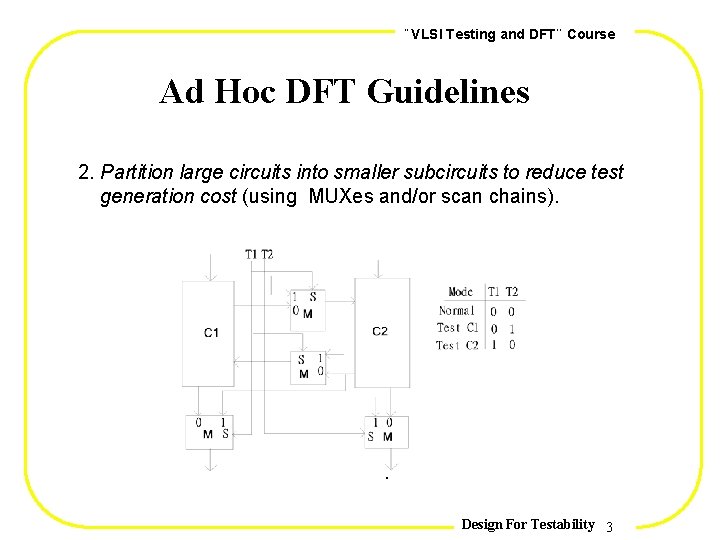
, , VLSI Testing and DFT Course Ad Hoc DFT Guidelines 2. Partition large circuits into smaller subcircuits to reduce test generation cost (using MUXes and/or scan chains). . Design For Testability 3
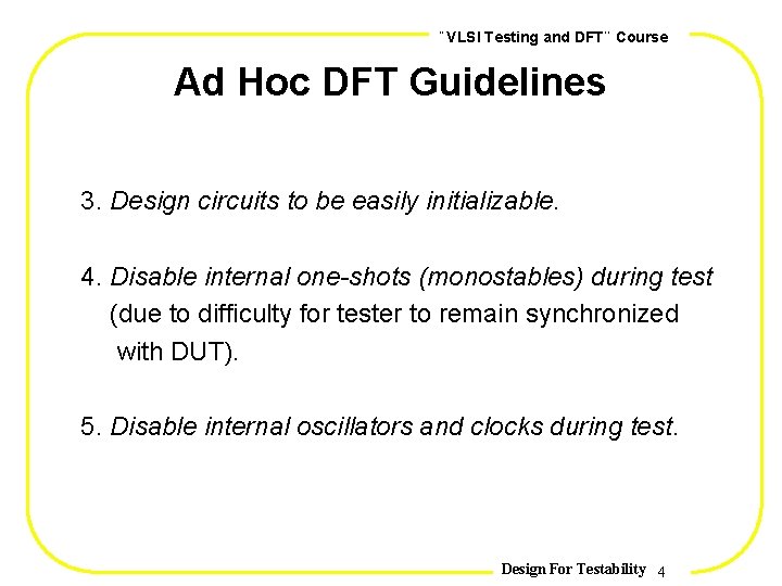
, , VLSI Testing and DFT Course Ad Hoc DFT Guidelines 3. Design circuits to be easily initializable. 4. Disable internal one-shots (monostables) during test (due to difficulty for tester to remain synchronized with DUT). 5. Disable internal oscillators and clocks during test. Design For Testability 4
, , VLSI Testing and DFT Course Ad Hoc DFT Guidelines 6. Partition large counters into smaller ones. 7. Avoid the use of redundant logic. 8. Provide logic to break global feedback paths. Design For Testability 5
, , VLSI Testing and DFT Course Ad Hoc DFT Guidelines 9. Keep analog and digital circuits physically apart. 10. Avoid the use of asynchronous logic. Design For Testability 6
, , VLSI Testing and DFT Course Ad Hoc DFT Guidelines 11. Avoid diagnostic ambiguity groups such as wired. OR/wired-AND junctions and highfanout nodes. 12. Consider tester requirements (pin limitation, tristating, etc. ) Design For Testability 7
, , VLSI Testing and DFT Course Ad Hoc DFT Guidelines • High fault coverage not guaranteed. • Manual test generation still required. • Design iterations also required. Design For Testability 8
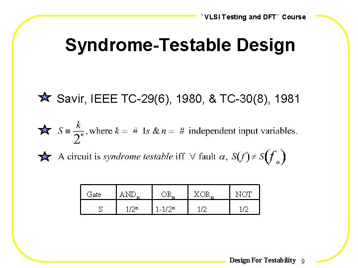
, , VLSI Testing and DFT Course Syndrome-Testable Design Savir, IEEE TC-29(6), 1980, & TC-30(8), 1981 Gate ANDn ORn S 1/2 n 1 -1/2 n XORn NOT 1/2 Design For Testability 9
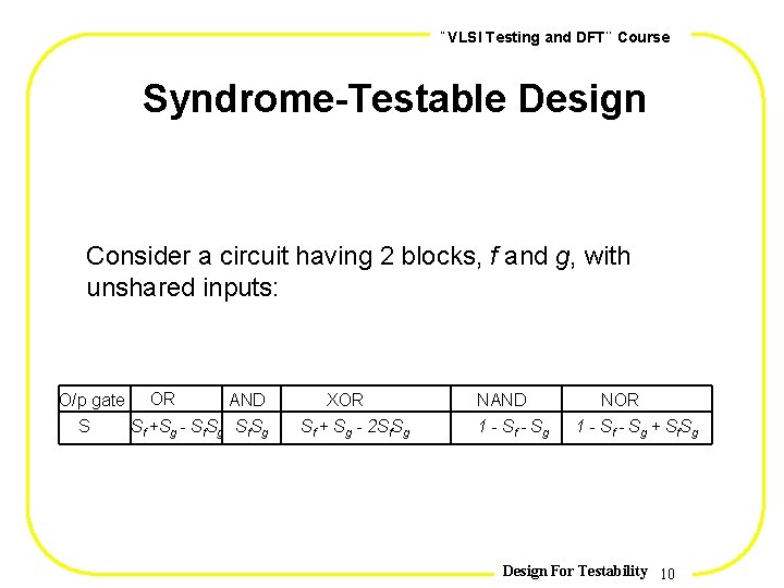
, , VLSI Testing and DFT Course Syndrome-Testable Design Consider a circuit having 2 blocks, f and g, with unshared inputs: O/p gate S OR AND Sf +Sg - Sf. Sg XOR Sf + Sg - 2 Sf. Sg NAND 1 - Sf - Sg NOR 1 - Sf - Sg + Sf. Sg Design For Testability 10
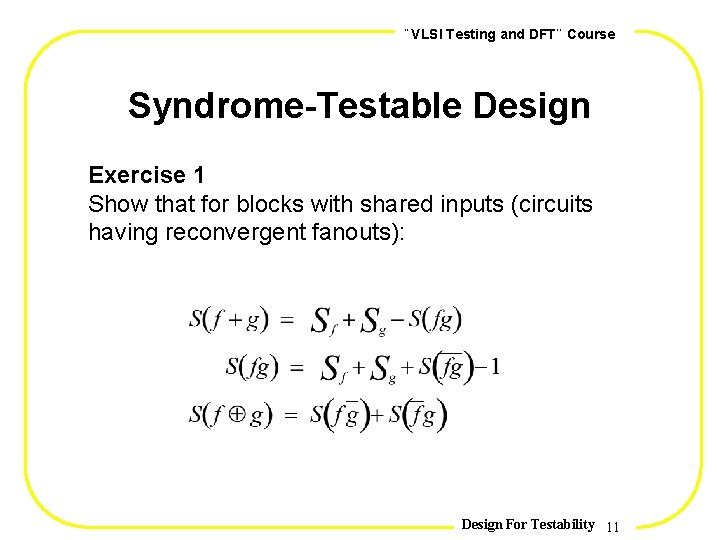
, , VLSI Testing and DFT Course Syndrome-Testable Design Exercise 1 Show that for blocks with shared inputs (circuits having reconvergent fanouts): Design For Testability 11
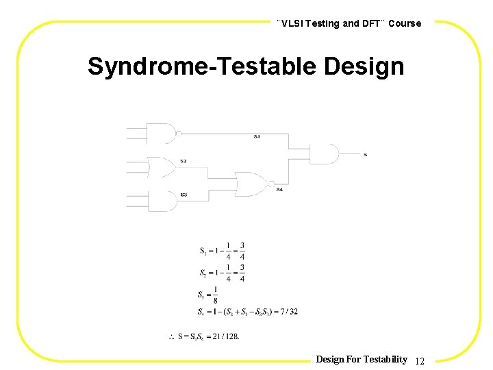
, , VLSI Testing and DFT Course Syndrome-Testable Design For Testability 12
, , VLSI Testing and DFT Course Syndrome-Testable Design Definition 1 A logic function is unate in a variable xi if it can be represented as an sop or pos expression in which the variable xi appears either only in an uncomplemented form or only in a complemented form. Theorem 1 A 2 -level irredundant circuit realizing a unate function in all its variables is syndrometestable. Theorem 2 Any 2 -level irredundant circuit can be made syndrome-testable by adding control inputs to the AND gates. Design For Testability 13
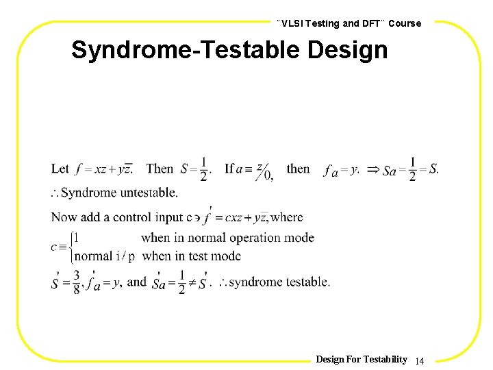
, , VLSI Testing and DFT Course Syndrome-Testable Design For Testability 14
, , VLSI Testing and DFT Course Syndrome-Testable Design Drawbacks: Only for combinational logic. Exhaustive: all patterns applied, and # of 1 s recorded. Only applicable to small circuits (larger circuits partition). Modification doubles test set size. Design For Testability 15
, , VLSI Testing and DFT Course Scan -Type Design • To provide controllability and observability of internal state variables for testing. • To turn the sequential test problem into a combinational one. Four Major Approaches: 1. Shift-register modification [M. Williams & Angell, IEEE TC-22(1), 1973]. 2. Scan path [Funatsu et al. , DA Symp. , 1975, & ITC, 1978]. 3. LSSD [Eichelberger & T. Williams, DAC, 1977, & JDAVTC-2(2), 1978]. 4. Random access [Ando, COMPCON, 1980]. Design For Testability 16
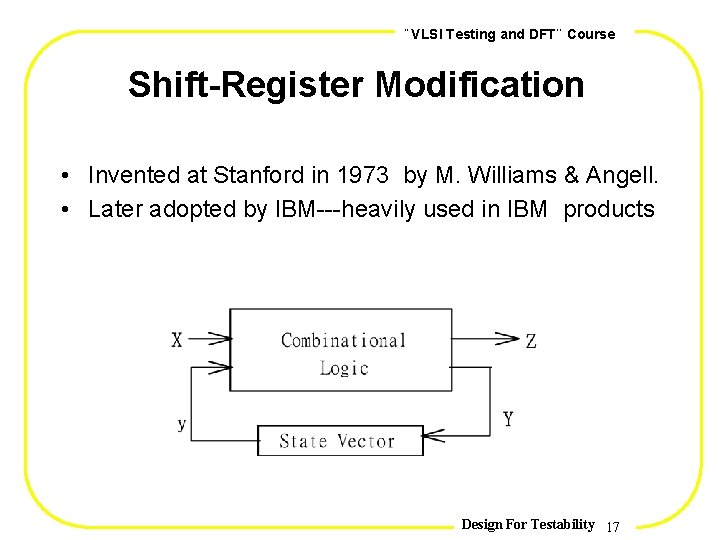
, , VLSI Testing and DFT Course Shift-Register Modification • Invented at Stanford in 1973 by M. Williams & Angell. • Later adopted by IBM---heavily used in IBM products Design For Testability 17
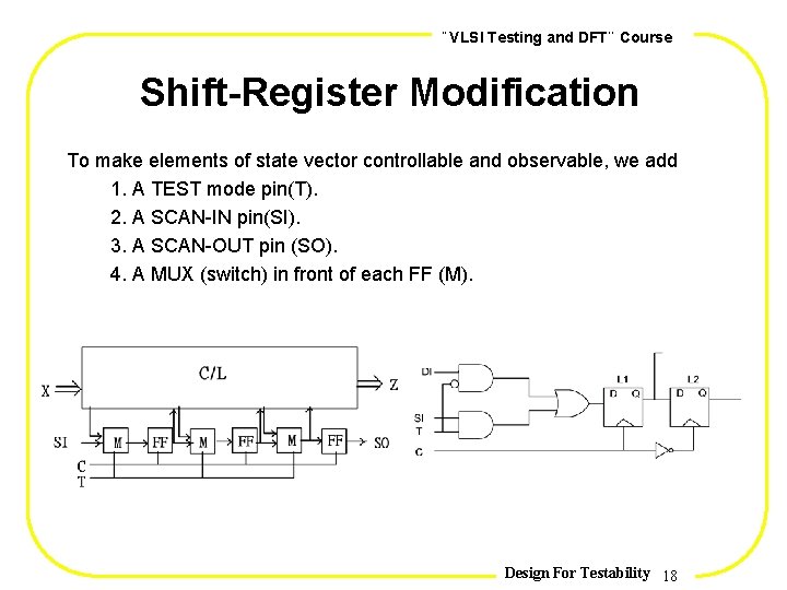
, , VLSI Testing and DFT Course Shift-Register Modification To make elements of state vector controllable and observable, we add 1. A TEST mode pin(T). 2. A SCAN-IN pin(SI). 3. A SCAN-OUT pin (SO). 4. A MUX (switch) in front of each FF (M). Design For Testability 18
, , VLSI Testing and DFT Course Shift-Register Modification Test procedure: 1. Switch to the shift-register mode and check the SR operation by shifting in an alternating sequence of 1 s and 0 s, e. g. , 00110 (functional test) 2. Initialize the SR---load the first pattern. 3. Return to the normal mode and apply the test pattern. 4. Switch to the SR mode and shift out the final state while setting the starting state for the next test. Go to 3. • The SI pin may be a redefined input pin (using a MUX ) in test mode. • The SO pin may be a redefined output pin (using a MUX ) in test mode. Design For Testability 19
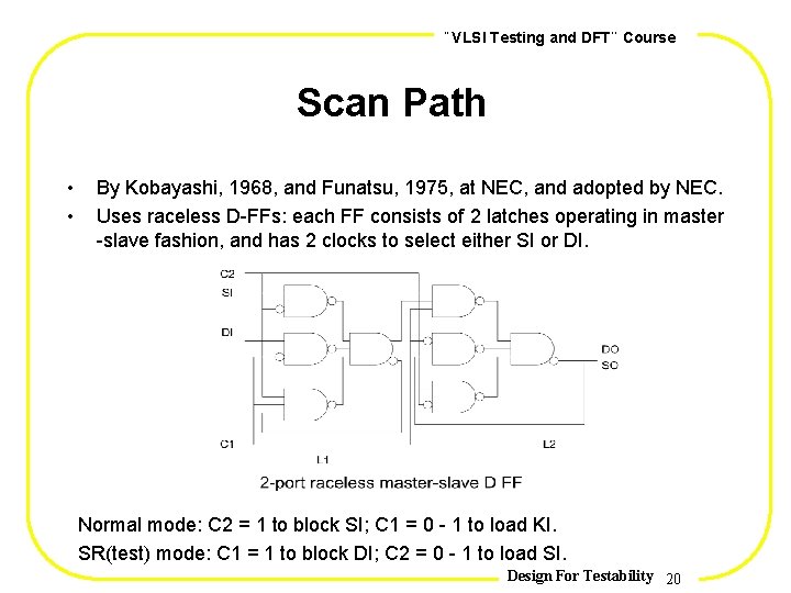
, , VLSI Testing and DFT Course Scan Path • • By Kobayashi, 1968, and Funatsu, 1975, at NEC, and adopted by NEC. Uses raceless D-FFs: each FF consists of 2 latches operating in master -slave fashion, and has 2 clocks to select either SI or DI. Normal mode: C 2 = 1 to block SI; C 1 = 0 - 1 to load KI. SR(test) mode: C 1 = 1 to block DI; C 2 = 0 - 1 to load SI. Design For Testability 20
, , VLSI Testing and DFT Course Level-Sensitive Scan Design (LSSD) • By Eichelberger and T. Williams, 1977, 1978 • Latch-based design used at IBM. • Race-& hazard-free operation and testing: insensitive to rise time, fall time, delay, etc. • Faster than SR modification; lower hardware complexity. • More complicated design rules. • Uses 2 latches: one for normal operation and one for scan. A logic circuit is level sensitive iff the steady state response to any allowed input change is independent of the delays within the circuit. Also, the response is independent of the order in which the inputs change. Design For Testability 21
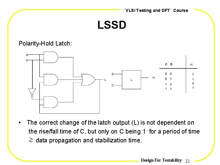
, , VLSI Testing and DFT Course LSSD Polarity-Hold Latch: • The correct change of the latch output (L) is not dependent on the rise/fall time of C, but only on C being , 1, for a period of time data propagation and stabilization time. Design For Testability 22
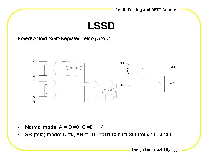
, , VLSI Testing and DFT Course LSSD Polarity-Hold Shift-Register Latch (SRL): • • Normal mode: A = B =0, C =0 SR (test) mode: C =0, AB = 10 1. 01 to shift SI through L 1 and L 2. Design For Testability 23
, , VLSI Testing and DFT Course LSSD • Polarity-Hold, hazard-free, and level-sensitive. • To be race-free, clocks C & B as well as A & B must be nonoverlapping. • Avoids performance degradation introduced by the MUX in shift-register modification. • Can replace B with A+B, i. e. , NOR(A, C). Design For Testability 24
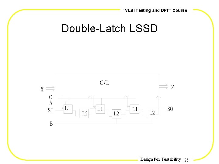
, , VLSI Testing and DFT Course Double-Latch LSSD Design For Testability 25
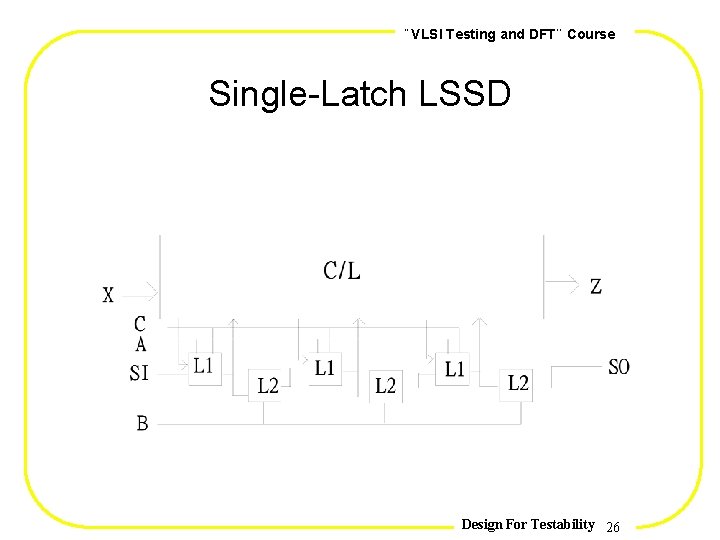
, , VLSI Testing and DFT Course Single-Latch LSSD Design For Testability 26
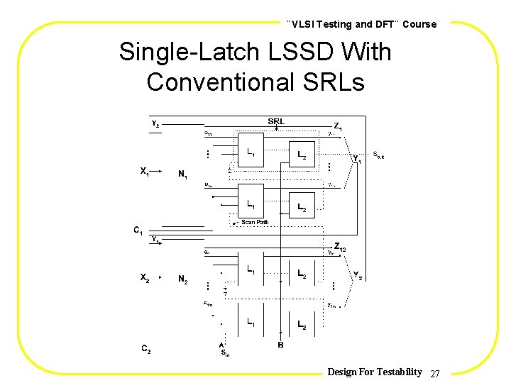
, , VLSI Testing and DFT Course Single-Latch LSSD With Conventional SRLs Design For Testability 27
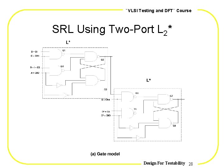
, , VLSI Testing and DFT Course SRL Using Two-Port L 2* Design For Testability 28
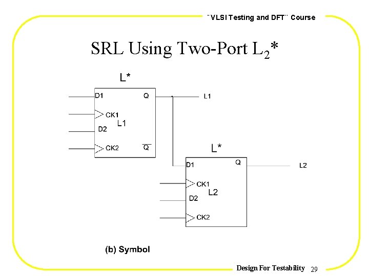
, , VLSI Testing and DFT Course SRL Using Two-Port L 2* Design For Testability 29
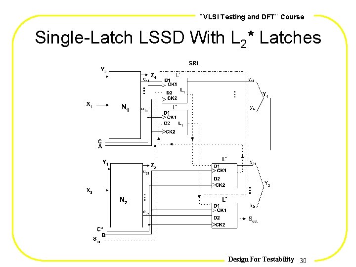
, , VLSI Testing and DFT Course Single-Latch LSSD With L 2* Latches Design For Testability 30
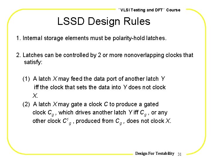
, , VLSI Testing and DFT Course LSSD Design Rules 1. Internal storage elements must be polarity-hold latches. 2. Latches can be controlled by 2 or more nonoverlapping clocks that satisfy: (1) A latch X may feed the data port of another latch Y iff the clock that sets the data into Y does not clock X. (2) A latch X may gate a clock C to produce a gated clock Cg , which drives another latch Y iff Cg , or any other clock C 1 g , produced from Cg , does not clock X. Design For Testability 31
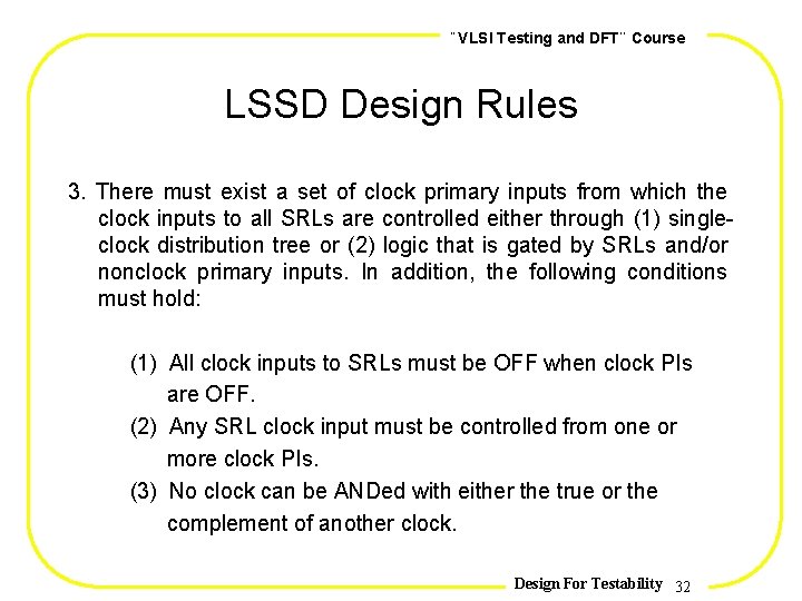
, , VLSI Testing and DFT Course LSSD Design Rules 3. There must exist a set of clock primary inputs from which the clock inputs to all SRLs are controlled either through (1) singleclock distribution tree or (2) logic that is gated by SRLs and/or nonclock primary inputs. In addition, the following conditions must hold: (1) All clock inputs to SRLs must be OFF when clock PIs are OFF. (2) Any SRL clock input must be controlled from one or more clock PIs. (3) No clock can be ANDed with either the true or the complement of another clock. Design For Testability 32
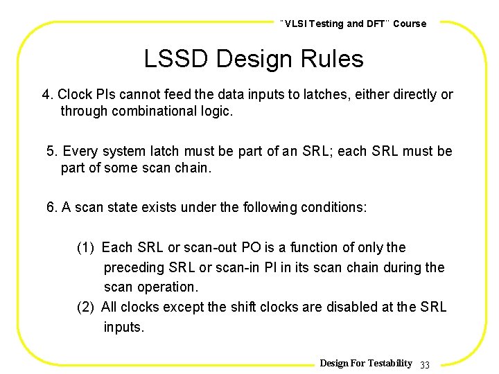
, , VLSI Testing and DFT Course LSSD Design Rules 4. Clock PIs cannot feed the data inputs to latches, either directly or through combinational logic. 5. Every system latch must be part of an SRL; each SRL must be part of some scan chain. 6. A scan state exists under the following conditions: (1) Each SRL or scan-out PO is a function of only the preceding SRL or scan-in PI in its scan chain during the scan operation. (2) All clocks except the shift clocks are disabled at the SRL inputs. Design For Testability 33
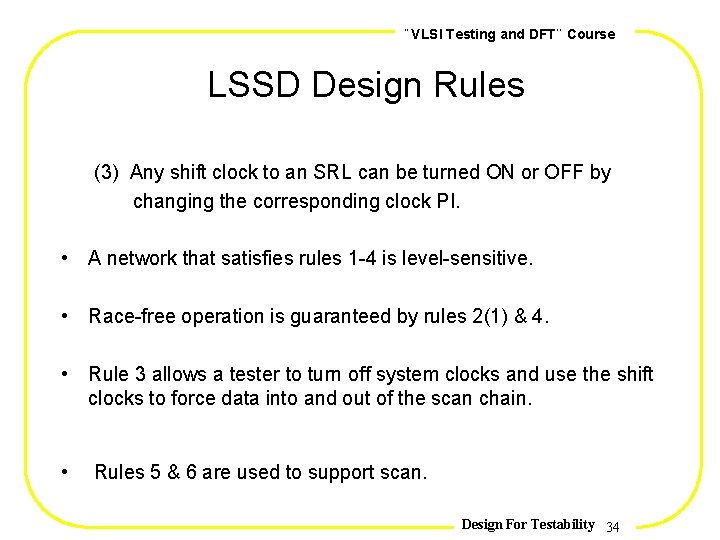
, , VLSI Testing and DFT Course LSSD Design Rules (3) Any shift clock to an SRL can be turned ON or OFF by changing the corresponding clock PI. • A network that satisfies rules 1 -4 is level-sensitive. • Race-free operation is guaranteed by rules 2(1) & 4. • Rule 3 allows a tester to turn off system clocks and use the shift clocks to force data into and out of the scan chain. • Rules 5 & 6 are used to support scan. Design For Testability 34
, , VLSI Testing and DFT Course Advantages With LSSD • Correct operation characteristics. independent of AC • Reducing FSM to C/L as far as testing is concerned. • Eliminating hazards & races; simplifying test generation and fault simulation. Design For Testability 35
, , VLSI Testing and DFT Course Problems With LSSD • Design rules imposed on designers --- no freedom to vary from the overall schemes, and higher design and hardware costs (420% more h/w & 4 extra pins). • No asynchronous designs. • Sequential routing of latches can introduce irregular structures. • Faults Changing combinational function to sequential may cause trouble, e. g. , bridging and CMOS stuck-open. • Function to be tested has been changed into a quite different combinational one, so specification language won, t be of any help. • Slow test application; normal-speed testing is impossible. • Not good for memory intensive designs. Design For Testability 36
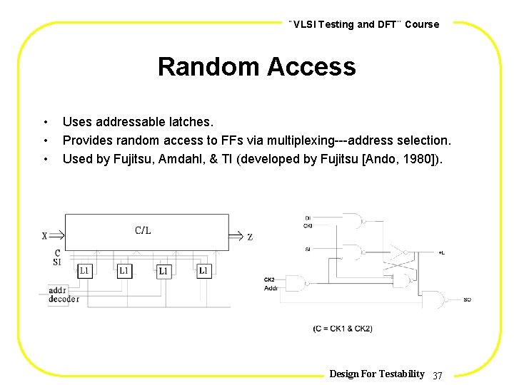
, , VLSI Testing and DFT Course Random Access • • • Uses addressable latches. Provides random access to FFs via multiplexing---address selection. Used by Fujitsu, Amdahl, & TI (developed by Fujitsu [Ando, 1980]). Design For Testability 37
, , VLSI Testing and DFT Course Random Access Advantages: Fast; minimal impact on normal path. Fast for testing---random access. Ability to , watch, a node in normal operation mode (impossible with LSSD). Disadvantages: Address decode---and thus h/w overhead---is large. More pins added (. . . parallel address). No asynchronous circuits. Design For Testability 38
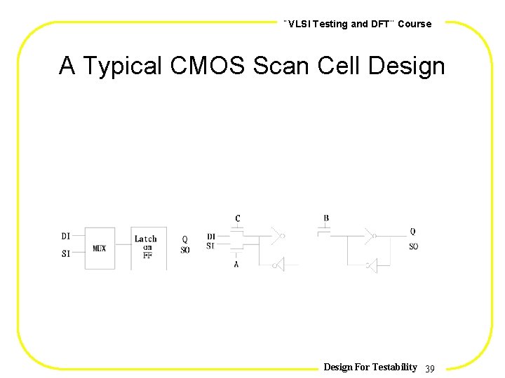
, , VLSI Testing and DFT Course A Typical CMOS Scan Cell Design For Testability 39
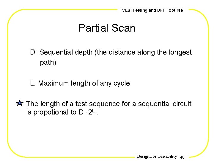
, , VLSI Testing and DFT Course Partial Scan D: Sequential depth (the distance along the longest path) L: Maximum length of any cycle The length of a test sequence for a sequential circuit is propotional to D. 2 L. Design For Testability 40
, , VLSI Testing and DFT Course Partial Scan BASIC IDEA Select a subset of flip-flops for scan Lower overhead (area and speed) Relaxed design rules METHOD 1 (Trischler et al, ITC-80) Use testability measure for flip-flop selection Use sequential ATPG METHOD 2 (Agrawal et al, D&T, April 1988) Use functional vectors for initial fault coverage Use comb. ATPG to select flip-flops for scan Overhead about 50% of full-scan METHOD 3 (Cheng and Agrawal, FTCS-19) Select scan flip-flops to simplify sequential ATPG Overhead about 25% of full scan Design For Testability 41
, , VLSI Testing and DFT Course Partial Scan (Cheng and Agrawal) • SELECT MINIMAL SET OF FLIP-FLOPS TO ELIMINATE SOME OR ALL CYCLES • SELF-LOOPS (CYCLES OF UNIT LENGTH) ARE NOT BROKEN TO KEEP THE SCAN OVERHEAD LOW – THE NUMBER OF SELF-LOOPS IN REAL DESIGN CAN BE QUITE LARGE Design For Testability 42
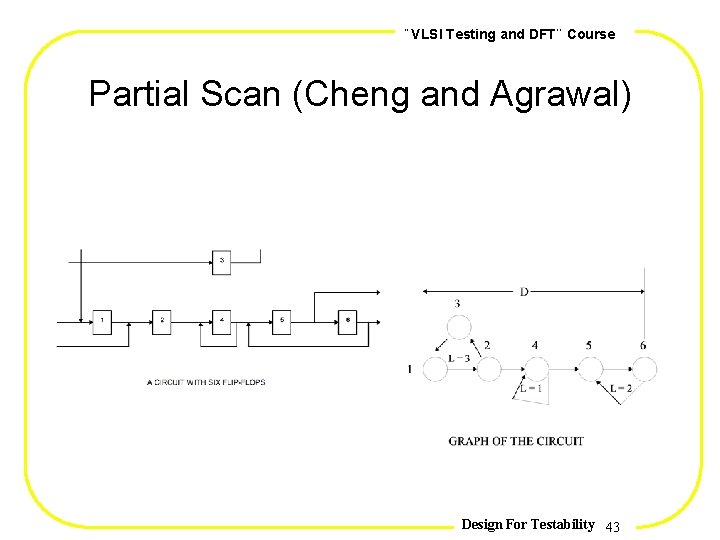
, , VLSI Testing and DFT Course Partial Scan (Cheng and Agrawal) Design For Testability 43
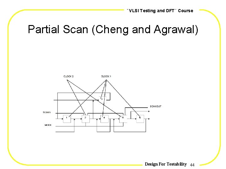
, , VLSI Testing and DFT Course Partial Scan (Cheng and Agrawal) Design For Testability 44
, , VLSI Testing and DFT Course Partial Scan (Cheng and Agrawal) • SEPARATE SCAN CLOCK IS USED • SCAN FLIP-FLOPS ARE REMOVED AND THEIR INPUT AND OUTPUT SIGNALS ARE ADDED TO THE PO/PI LISTS • A SEQUENTIAL CIRCUIT TEST GENERATOR IS USED FOR TEST GENERATION • THE VECTOR SEQUENCES ARE THEN CONVERTED INTO SCAN SEQUENCES: • EACH VECTOR IS PRECEDED BY A SCAN-IN SEQUENCE TO SET THE STATES OF SCANNED FLIP -FLOPS • A SCAN-OUT SEQUENCE IS ADDED AT THE END OF EACH VECTOR SEQUENCE Design For Testability 45
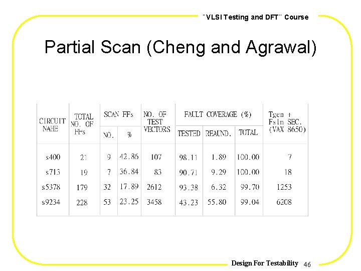
, , VLSI Testing and DFT Course Partial Scan (Cheng and Agrawal) Design For Testability 46
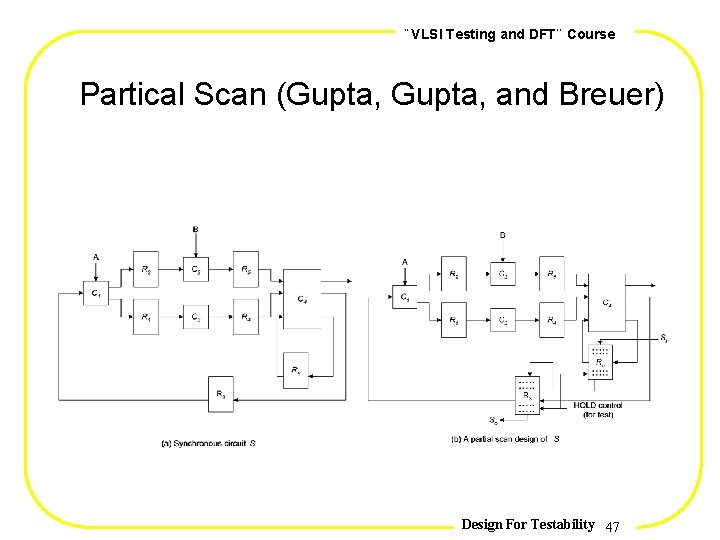
, , VLSI Testing and DFT Course Partical Scan (Gupta, and Breuer) Design For Testability 47
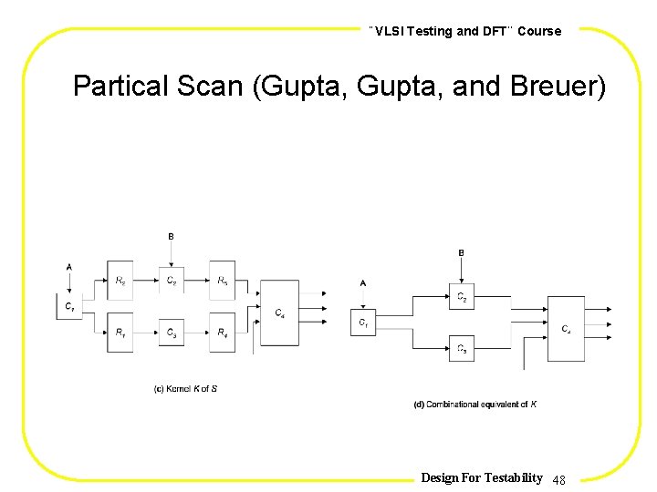
, , VLSI Testing and DFT Course Partical Scan (Gupta, and Breuer) Design For Testability 48
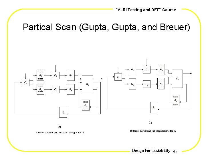
, , VLSI Testing and DFT Course Partical Scan (Gupta, and Breuer) Design For Testability 49
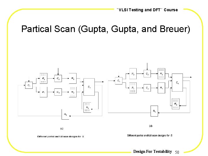
, , VLSI Testing and DFT Course Partical Scan (Gupta, and Breuer) Design For Testability 50
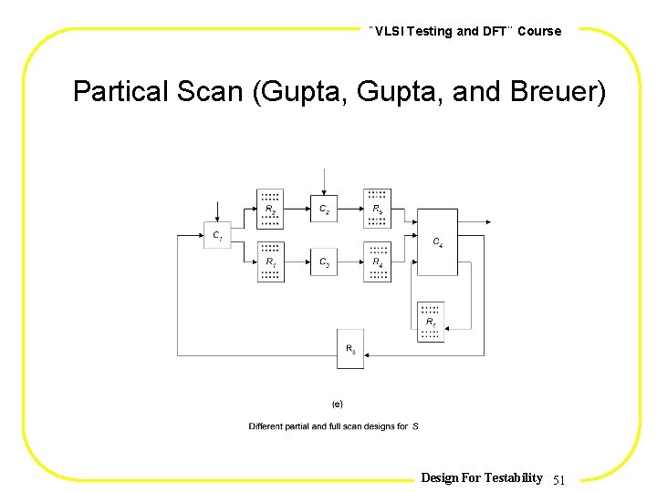
, , VLSI Testing and DFT Course Partical Scan (Gupta, and Breuer) Design For Testability 51
- Slides: 51