VLSI Systems Design Lecture 1 Introduction Engr Anees


- Slides: 24

VLSI Systems Design Lecture: 1 Introduction Engr. Anees ul Husnain ( anees. buzdar@gmail. com ) Department of Computer Systems Engineering, College of Engineering & Technology, IUB

Lecture’s Goals o General Introduction to VLSI Systems o Introduction to MOS o Why you should be able to understand such systems. o How much these systems are in our lives.

Books on VLSI Text Books: 1. CMOS VLSI, A circuit & Systems Prospective By David Haris & Neil Weste 2. Design through verilog HDL By T. R. Padmanabhan. B. Bala Tripura Sundari Softwares: Micro-wind, Xilinx ISE

Introduction Lecturer: Office : Engr. Anees ul Husnain Email: URL: anees. buzdar@gmail. com http: //www. iub. edu. pk Dept. of Computer Systems Engineering, UCET - IUB

Grade Breakdown Homework: Quiz 1: Quiz 2: Quiz 3: 30 20 20 30 % % *Every student is expected to attend all of the lectures to get full marks

Online Collaboration… o www. groups. yahoo. com/group/UCET_VLSI o o o Lecture slides Homework Results Reading materials Practical / Lab work o Important announcements o Course Discussions, etc.

Course Breakup… o Course breakup file

Laboratory o Micro-wind layout and simulation package o Dedicated to training in sub-micron design rules for CMOS VLSI design o Layout editor, electrical circuit extractor. o Designing through HDLs & Burning on IC (FPGA)

Learning Outcomes o Understand the principles of the design and implementation of standard MOS integrated circuits and be able to assess their performance taking into account the effects of real circuit parameters.

Why VLSI? o Integration improves the design n Lower parasitics = higher speed Lower power consumption Physically smaller o Integration reduces manufacturing cost - (almost) no manual assembly

Introduction to VLSI Technology • • Introduction • Typical Applications • Moore’s Law • The cost of fabrication Technology Background

VLSI Applications o VLSI is an implementation technology for electronic circuitry - analogue or digital o It is concerned with forming a pattern of interconnected switches and gates on the surface of a crystal of semiconductor o Microprocessors n personal computers n microcontrollers o o Memory - DRAM / SRAM Special Purpose Processors - ASICS (CD players, DSP applications) Optical Switches Has made highly sophisticated control systems mass-producable and therefore cheap

Moore’s Law o Gordon Moore: co-founder of Intel o Predicted that the number of transistors per chip would grow exponentially (double every 18 months) o Exponential improvement in technology is a natural trend: n e. g. Steam Engines - Dynamo - Automobile

The Cost of Fabrication o Current cost $2 - 3 billion o Typical fab line occupies 1 city block, employees a few hundred employees o Most profitable period is first 18 months to 2 years o For large volume IC’s packaging and testing is largest cost o For low volume IC’s, design costs may swamp manufacturing costs

Technology Background… • What is a chip • Switches • Doping • IC Technology • Basic MOS Transistor • Fabrication Technology • CMOS Technology • Bi-CMOS

What is a Silicon Chip? o A pattern of interconnected switches and gates on the surface of a crystal of semiconductor (typically Si) o These switches and gates are made of n n areas of n-type silicon areas of p-type silicon areas of insulator lines of conductor (interconnects) joining areas together o Aluminium, Copper, Titanium, Molybdenum, polysilicon, tungsten o The geometry of these areas is known as the layout of the chip o Connections from the chip to the outside world are made around the edge of the chip to facilitate connections to other devices

Switches o Digital equipment is largely composed of switches o Switches can be built from many technologies n relays (from which the earliest computers were built) n thermionic valves n transistors o The perfect digital switch would have the following: n n n switch instantly use no power have an infinite resistance when off and zero resistance when on o Real switches are not like this!

Semiconductors and Doping o Adding trace amounts of certain materials to semiconductors alters the crystal structure and can change their electrical properties n o N-Type n n o semiconductor has free electrons dopant is (typically) phosphorus, arsenic, antimony P-Type n n o in particular it can change the number of free electrons or holes semiconductor has free holes dopant is (typically) boron, indium, gallium Dopants are usually implanted into the semiconductor using Implant Technology, followed by thermal process to diffuse the dopants

IC Technology o Speed / Power performance of available technologies o The microelectronics evolution o SIA Roadmap (Semiconductor Industry Association) o Semiconductor Manufacturers 2010 Ranking ? ? ?

Metal-oxide-semiconductor (MOS) and related VLSI technology o o o p. MOS n. MOS CMOS Bi. CMOS Ga. As

Basic MOS Transistors o Minimum line width o Transistor cross section o Charge inversion channel o Source connected to substrate o p. MOS are 2. 5 time slower than n. MOS due to electron and hole mobilities

Fabrication Technology o Silicon of extremely high purity n chemically purified then grown into large crystals o Wafers n n crystals are sliced into wafers wafer diameter is currently 150 mm, 200 mm, 300 mm wafer thickness <1 mm surface is polished to optical smoothness o Wafer is then ready for processing o Each wafer will yield many chips n n chip die size varies from about 5 mmx 5 mm to 15 mmx 15 mm A whole wafer is processed at a time n Fabrication technology will be covered in detail with video sessions in chapter 3

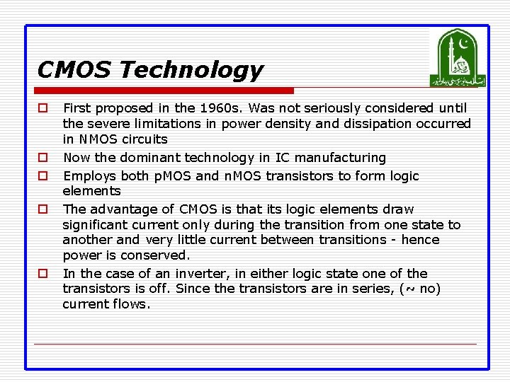
CMOS Technology o o o First proposed in the 1960 s. Was not seriously considered until the severe limitations in power density and dissipation occurred in NMOS circuits Now the dominant technology in IC manufacturing Employs both p. MOS and n. MOS transistors to form logic elements The advantage of CMOS is that its logic elements draw significant current only during the transition from one state to another and very little current between transitions - hence power is conserved. In the case of an inverter, in either logic state one of the transistors is off. Since the transistors are in series, (~ no) current flows.

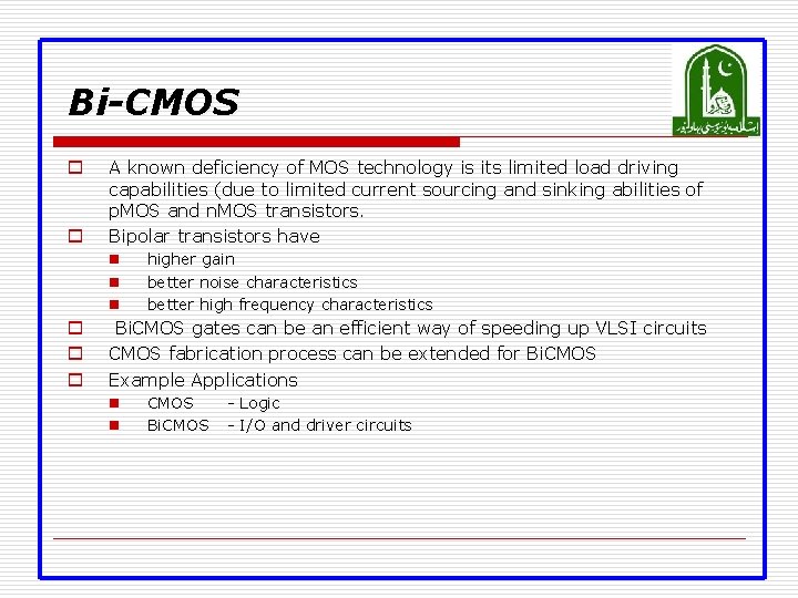
Bi-CMOS o o A known deficiency of MOS technology is its limited load driving capabilities (due to limited current sourcing and sinking abilities of p. MOS and n. MOS transistors. Bipolar transistors have n n n o o o higher gain better noise characteristics better high frequency characteristics Bi. CMOS gates can be an efficient way of speeding up VLSI circuits CMOS fabrication process can be extended for Bi. CMOS Example Applications n n CMOS Bi. CMOS - Logic - I/O and driver circuits