
VLSI Prof Vojin G Oklobdzija References used for
VLSI Prof. Vojin G. Oklobdzija References (used for creation of the presentation material): [1] Mead, Conway, “Introduction to VLSI Systems”, Addison Wesley Publishing. [2] Glasser, Dobberpuhl, “The Design and Analysis of VLSI Circuits”, Addison Wesley Publishing. [3] Weste, Eshraghian, “Principles of CMOS VLSI Design”, Addison Wesley Publishing. [4] Shoji, “CMOS Digital Circuits Technology”, Prentice Hall. Fall 2004 Prof. V. G. Oklobdzija: High. Performance System Design
Historical Overview • • n. MOS era: 1970 -85 Pass-transistor design CMOS existed early but took off 1985 on Domino CMOS, 1982 – NORA – DCVSL • CPL, DPL – DCVS-PG – SRPL – LEAP • SOI-CMOS Fall 2004 Prof. V. G. Oklobdzija: High-Performance System Design 2
n-MOS Design Era 1970 -85 LSI started with n. MOS: • pass-transistor design experience: - Flourished at the beginning of the n. MOS era (popularized by Mead-Conway book) - Allows high density layout and compact design style - Fast: outperforming gate based design - Low in power • Drawbacks: – Not compatible with existing design tools – Exhibiting testability and reliability problems Fall 2004 Prof. V. G. Oklobdzija: High-Performance System Design 3
Review of CMOS Prof. Vojin G. Oklobdzija Fall 2004 Prof. V. G. Oklobdzija: High. Performance System Design
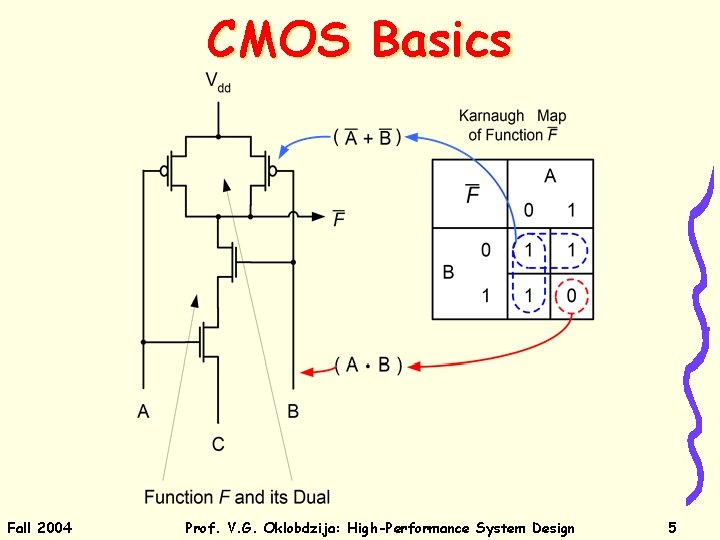
CMOS Basics Fall 2004 Prof. V. G. Oklobdzija: High-Performance System Design 5
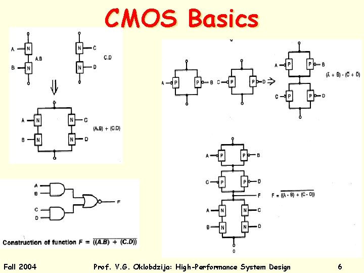
CMOS Basics Fall 2004 Prof. V. G. Oklobdzija: High-Performance System Design 6
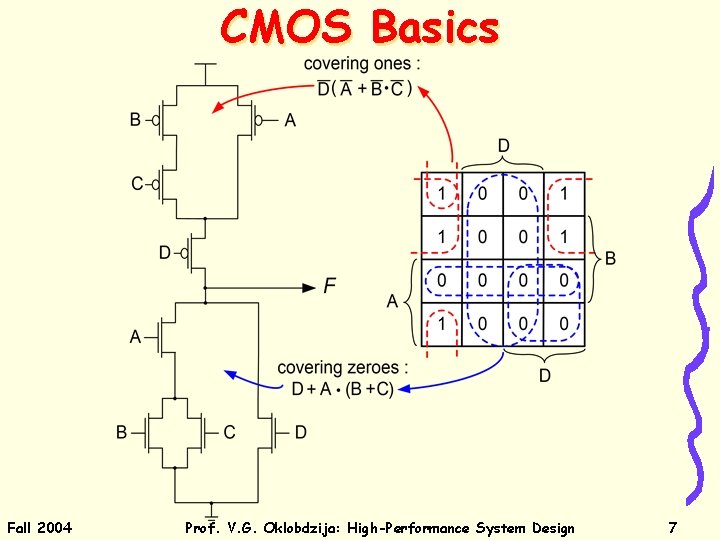
CMOS Basics Fall 2004 Prof. V. G. Oklobdzija: High-Performance System Design 7
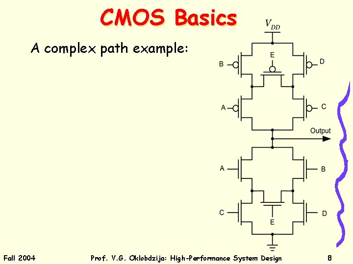
CMOS Basics A complex path example: Fall 2004 Prof. V. G. Oklobdzija: High-Performance System Design 8
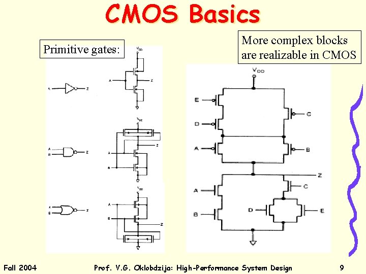
CMOS Basics Primitive gates: Fall 2004 More complex blocks are realizable in CMOS Prof. V. G. Oklobdzija: High-Performance System Design 9
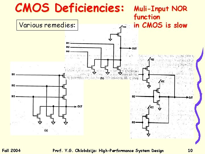
CMOS Deficiencies: Various remedies: Fall 2004 Muli-Input NOR function in CMOS is slow Prof. V. G. Oklobdzija: High-Performance System Design 10
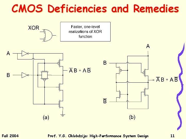
CMOS Deficiencies and Remedies Fall 2004 Prof. V. G. Oklobdzija: High-Performance System Design 11
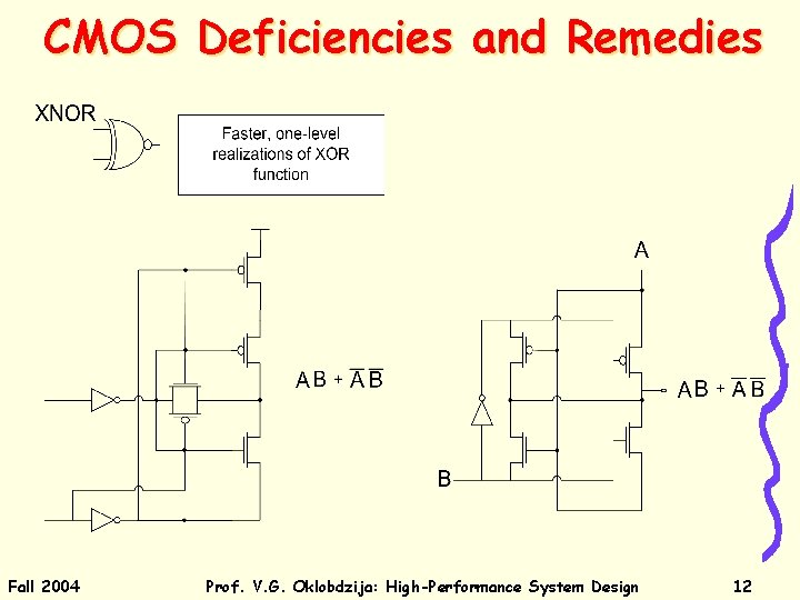
CMOS Deficiencies and Remedies Fall 2004 Prof. V. G. Oklobdzija: High-Performance System Design 12
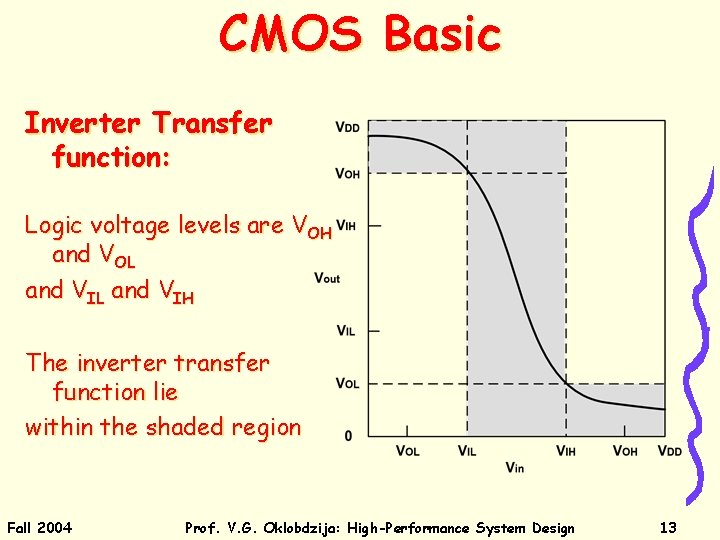
CMOS Basic Inverter Transfer function: Logic voltage levels are VOH and VOL and VIH The inverter transfer function lie within the shaded region Fall 2004 Prof. V. G. Oklobdzija: High-Performance System Design 13
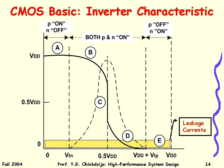
CMOS Basic: Inverter Characteristic Leakage Currents Fall 2004 Prof. V. G. Oklobdzija: High-Performance System Design 14
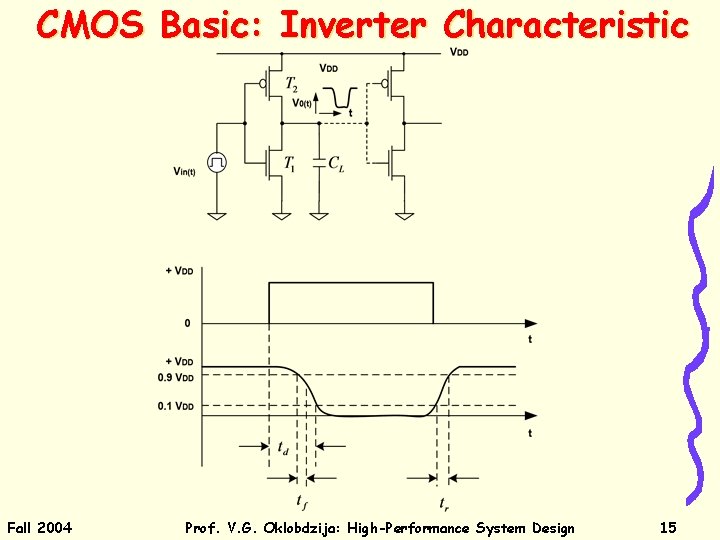
CMOS Basic: Inverter Characteristic Fall 2004 Prof. V. G. Oklobdzija: High-Performance System Design 15
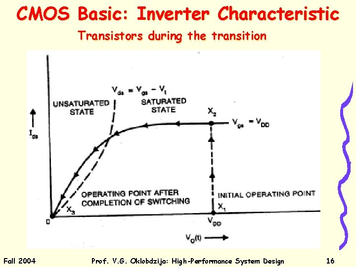
CMOS Basic: Inverter Characteristic Transistors during the transition Fall 2004 Prof. V. G. Oklobdzija: High-Performance System Design 16
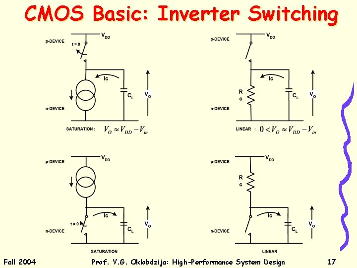
CMOS Basic: Inverter Switching Fall 2004 Prof. V. G. Oklobdzija: High-Performance System Design 17
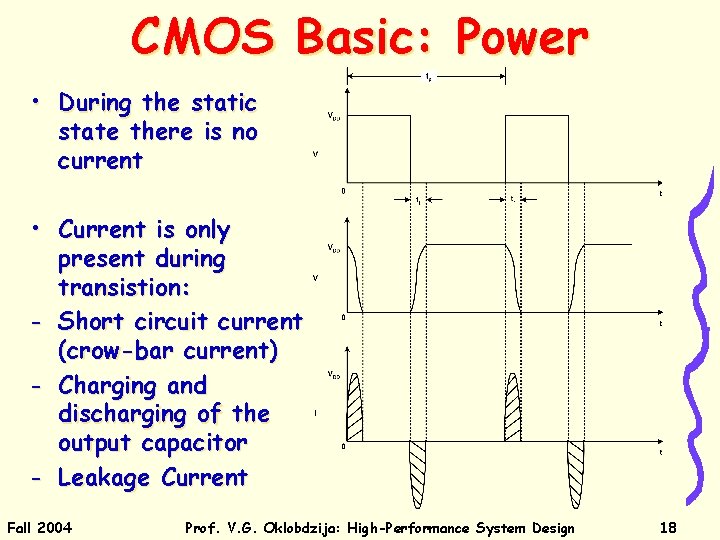
CMOS Basic: Power • During the static state there is no current • Current is only present during transistion: - Short circuit current (crow-bar current) - Charging and discharging of the output capacitor - Leakage Current Fall 2004 Prof. V. G. Oklobdzija: High-Performance System Design 18
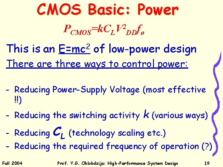
CMOS Basic: Power PCMOS=k. CLV 2 DDfo This is an E=mc 2 of low-power design There are three ways to control power: - Reducing Power-Supply Voltage (most effective !!) - Reducing the switching activity k (various ways) - Reducing CL (technology scaling etc. ) - Reducing the required frequency of operation (? ) Fall 2004 Prof. V. G. Oklobdzija: High-Performance System Design 19
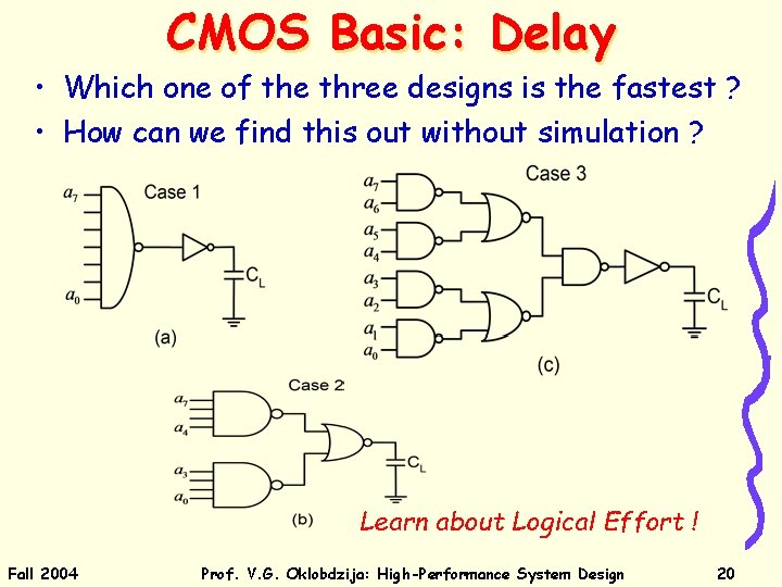
CMOS Basic: Delay • Which one of the three designs is the fastest ? • How can we find this out without simulation ? Learn about Logical Effort ! Fall 2004 Prof. V. G. Oklobdzija: High-Performance System Design 20
CMOS Basic: Delay Fall 2004 Prof. V. G. Oklobdzija: High-Performance System Design 21
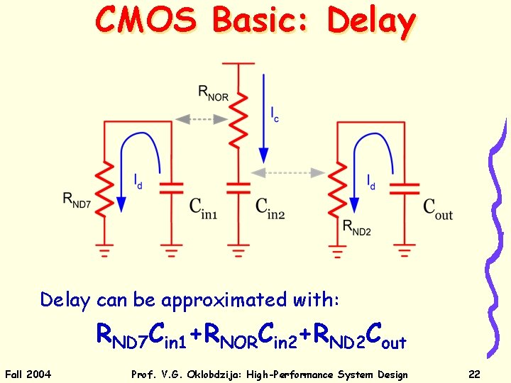
CMOS Basic: Delay can be approximated with: RND 7 Cin 1+RNORCin 2+RND 2 Cout Fall 2004 Prof. V. G. Oklobdzija: High-Performance System Design 22
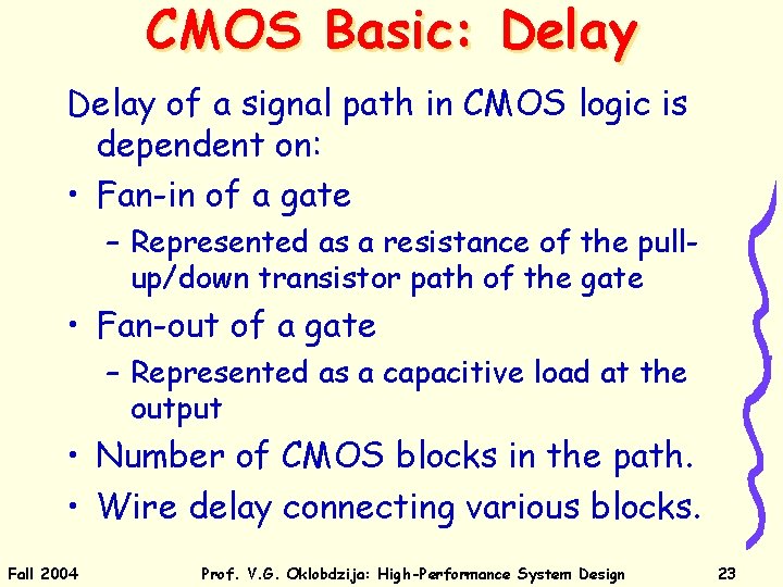
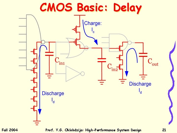
CMOS Basic: Delay of a signal path in CMOS logic is dependent on: • Fan-in of a gate – Represented as a resistance of the pullup/down transistor path of the gate • Fan-out of a gate – Represented as a capacitive load at the output • Number of CMOS blocks in the path. • Wire delay connecting various blocks. Fall 2004 Prof. V. G. Oklobdzija: High-Performance System Design 23
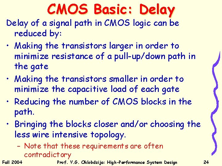
CMOS Basic: Delay of a signal path in CMOS logic can be reduced by: • Making the transistors larger in order to minimize resistance of a pull-up/down path in the gate • Making the transistors smaller in order to minimize the capacitive load of each gate • Reducing the number of CMOS blocks in the path. • Bringing the blocks closer and/or choosing the less wire intensive topology. – Note that these requirements are often contradictory Fall 2004 Prof. V. G. Oklobdzija: High-Performance System Design 24
CMOS Basic: Delay • How to estimate delay and critical timing in CMOS circuits ? • How to determine the proper transistor sizing in order to make a compromise with contradicting requirements ? • How to choose the right circuit topology ? The Answer: “Logical Effort” Fall 2004 Prof. V. G. Oklobdzija: High-Performance System Design 25
Pass-Transistor Design Fall 2004 Prof. V. G. Oklobdzija: High-Performance System Design 26
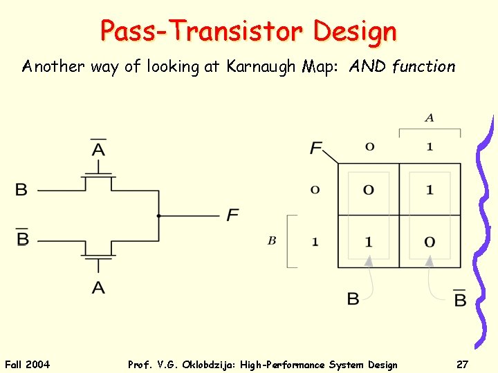
Pass-Transistor Design Another way of looking at Karnaugh Map: AND function Fall 2004 Prof. V. G. Oklobdzija: High-Performance System Design 27
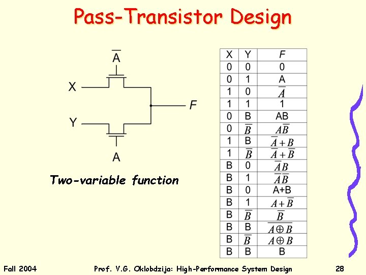
Pass-Transistor Design Two-variable function Fall 2004 Prof. V. G. Oklobdzija: High-Performance System Design 28
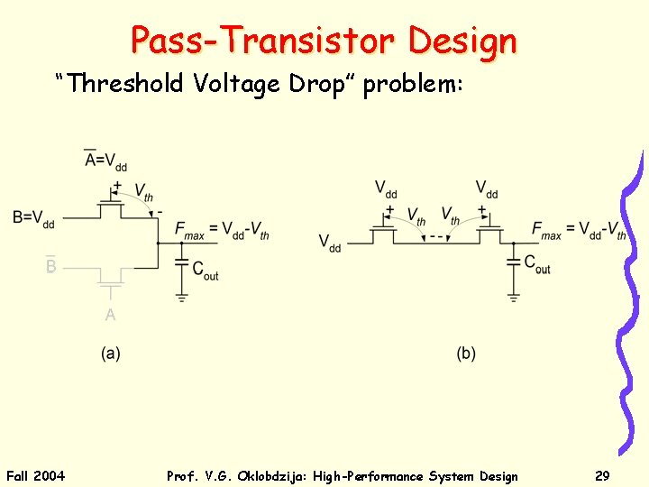
Pass-Transistor Design “Threshold Voltage Drop” problem: Fall 2004 Prof. V. G. Oklobdzija: High-Performance System Design 29
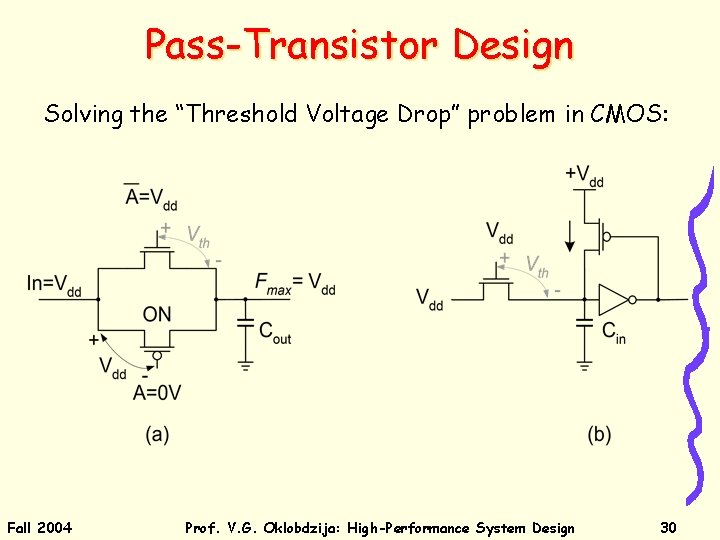
Pass-Transistor Design Solving the “Threshold Voltage Drop” problem in CMOS: Fall 2004 Prof. V. G. Oklobdzija: High-Performance System Design 30
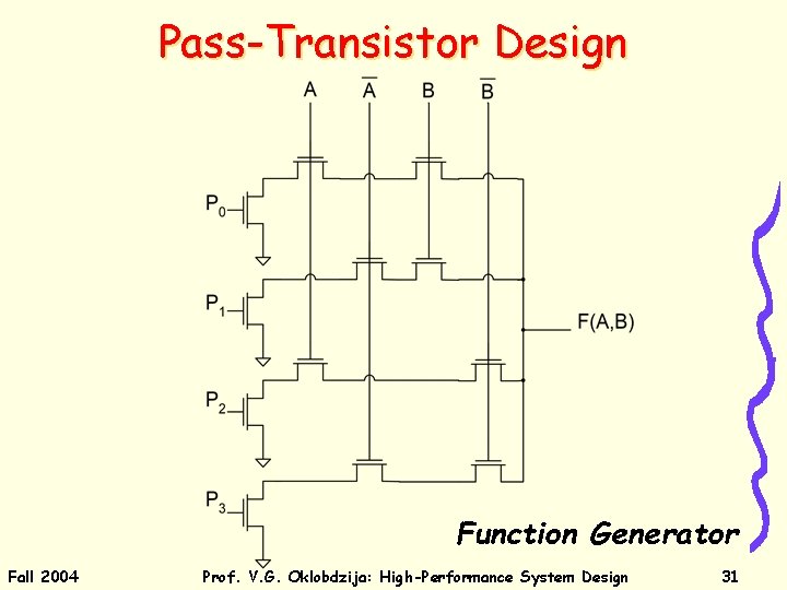
Pass-Transistor Design Function Generator Fall 2004 Prof. V. G. Oklobdzija: High-Performance System Design 31
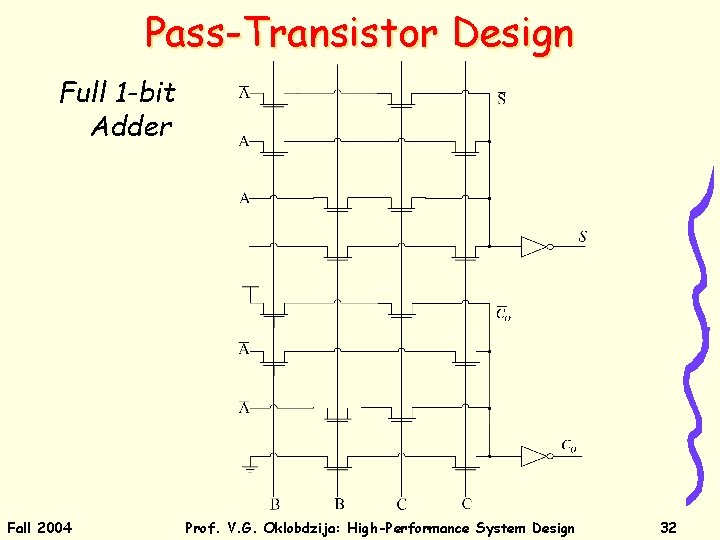
Pass-Transistor Design Full 1 -bit Adder Fall 2004 Prof. V. G. Oklobdzija: High-Performance System Design 32
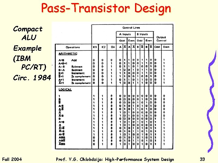
Pass-Transistor Design Compact ALU Example (IBM PC/RT) Circ. 1984 Fall 2004 Prof. V. G. Oklobdzija: High-Performance System Design 33
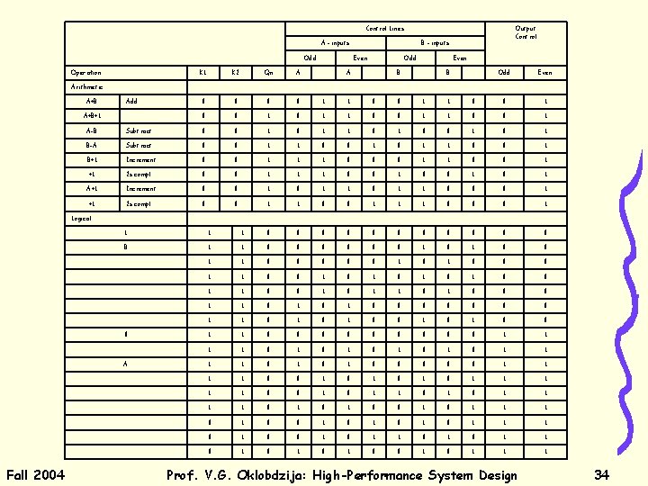
Control Lines A - inputs Odd Operation Output Control B - inputs Even Odd A Even K 1 K 2 Qn A B B Odd Even 0 0 1 1 0 0 1 Arithmetic A+B Add A+B+1 A-B Subtract 0 0 1 1 0 0 1 B-A Subtract 0 0 1 1 0 0 1 B+1 Increment 0 0 1 1 1 0 0 0 1 1 0 0 1 2 s compl 0 0 1 1 1 0 0 1 0 1 Increment 0 0 1 1 0 0 0 1 2 s compl 0 0 1 1 1 0 0 0 1 +1 A+1 +1 Logical 1 1 1 0 0 0 B 1 1 0 0 0 1 0 0 0 1 1 0 0 1 0 1 0 0 1 1 0 0 0 1 1 0 1 0 0 1 0 0 1 1 0 0 0 0 0 1 1 0 1 0 1 0 1 0 0 0 1 1 0 0 1 0 1 1 1 1 0 1 0 0 1 0 1 1 0 1 0 1 1 1 0 A Fall 2004 Prof. V. G. Oklobdzija: High-Performance System Design 34
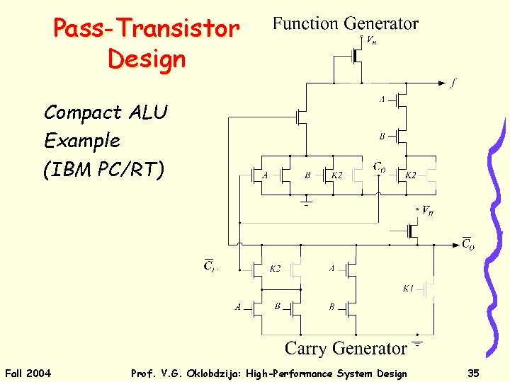
Pass-Transistor Design Compact ALU Example (IBM PC/RT) Fall 2004 Prof. V. G. Oklobdzija: High-Performance System Design 35
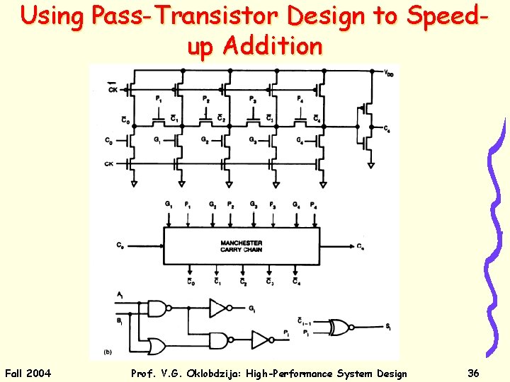
Using Pass-Transistor Design to Speedup Addition Fall 2004 Prof. V. G. Oklobdzija: High-Performance System Design 36
- Slides: 36