VLSI Physical Design Automation Lecture 2 Review of

![Example: Selection Sort • Input: An array of n numbers D[1]…D[n]. • Output: An Example: Selection Sort • Input: An array of n numbers D[1]…D[n]. • Output: An](https://slidetodoc.com/presentation_image/49d63b39714a60bf670700ebf26cf7ce/image-31.jpg)
- Slides: 42

VLSI Physical Design Automation Lecture 2. Review of Device/VLSI/Algorithm Prof. David Pan dpan@ece. utexas. edu Office: ACES 5. 434 11/3/2020 1

Objective of this Lecture a. To review the materials used in fabrication of VLSI devices. a. To review the structure of devices and process involved in fabricating different types of VLSI circuits a. To review the basic algorithm concepts a. To level-set everyone so that we can get into serious Physical Design topics in the next lecture 11/3/2020 2

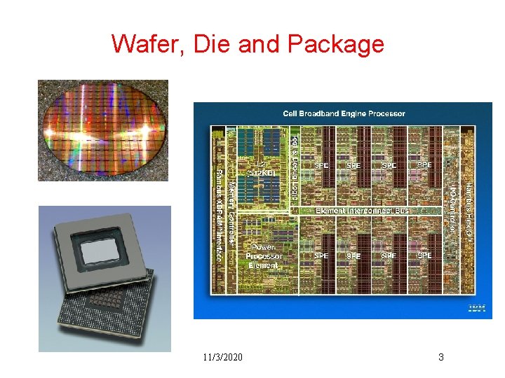
Wafer, Die and Package 11/3/2020 3

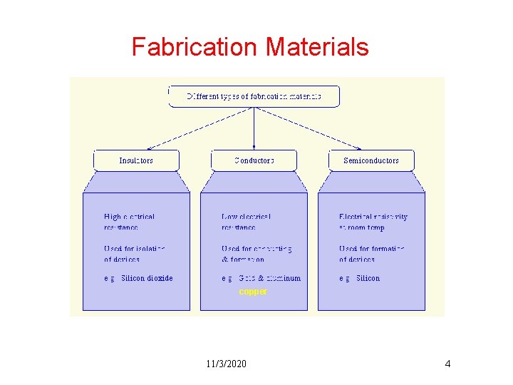
Fabrication Materials copper 11/3/2020 4

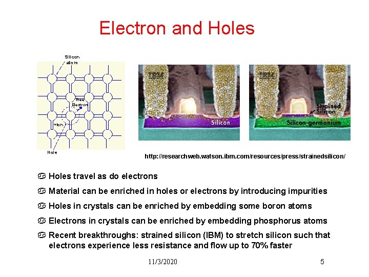
Electron and Holes Silicon atom Free Electron +Ion Hole http: //researchweb. watson. ibm. com/resources/press/strainedsilicon/ a Holes travel as do electrons a Material can be enriched in holes or electrons by introducing impurities a Holes in crystals can be enriched by embedding some boron atoms a Electrons in crystals can be enriched by embedding phosphorus atoms a Recent breakthroughs: strained silicon (IBM) to stretch silicon such that electrons experience less resistance and flow up to 70% faster 11/3/2020 5

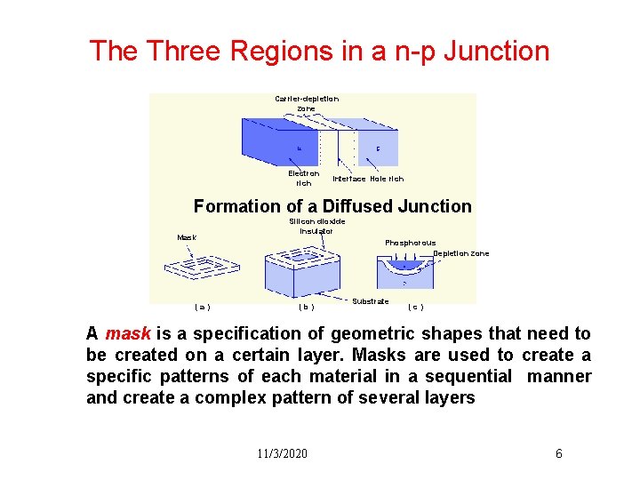
The Three Regions in a n-p Junction Carrier-depletion zone Electron rich Interface Hole rich Formation of a Diffused Junction Mask (a) Silicon dioxide insulator Phosphorous Depletion zone (b) Substrate (c) A mask is a specification of geometric shapes that need to be created on a certain layer. Masks are used to create a specific patterns of each material in a sequential manner and create a complex pattern of several layers 11/3/2020 6

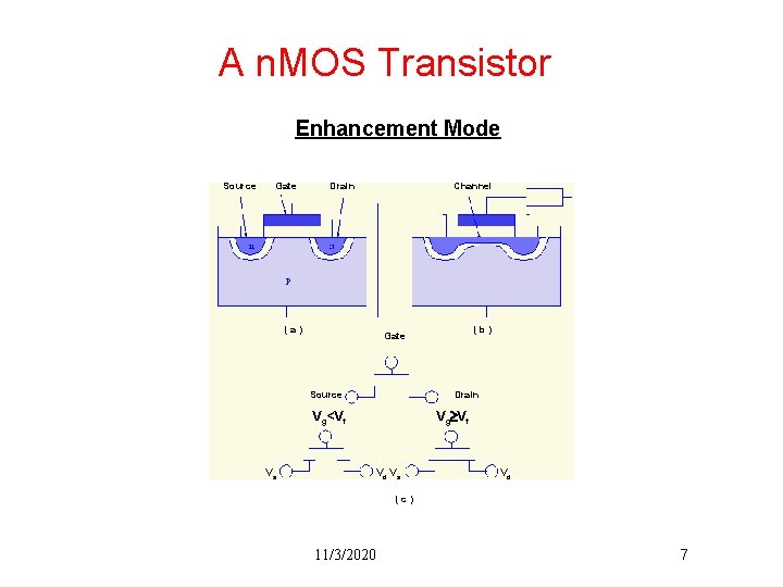
A n. MOS Transistor Enhancement Mode Source Gate Drain Channel (a) Source Drain Vg Vt Vg<Vt Vs (b) Gate Vd Vs Vd (c) 11/3/2020 7

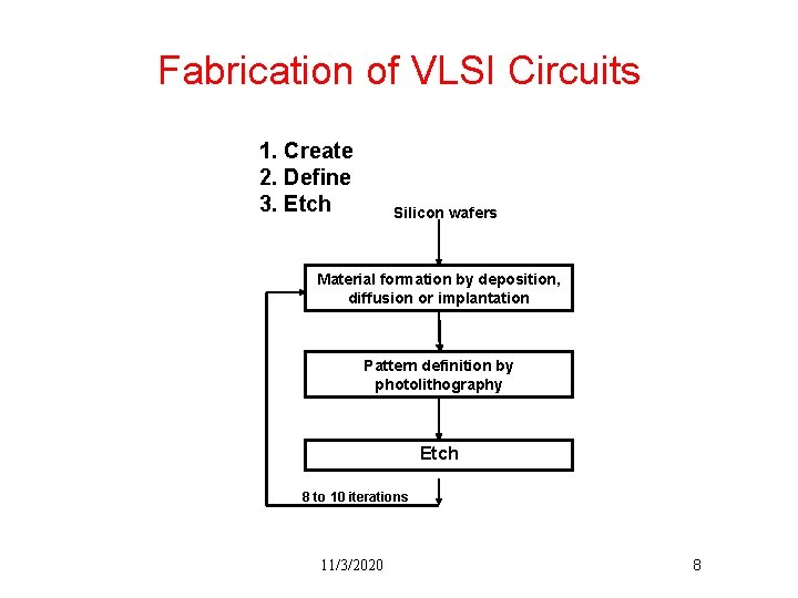
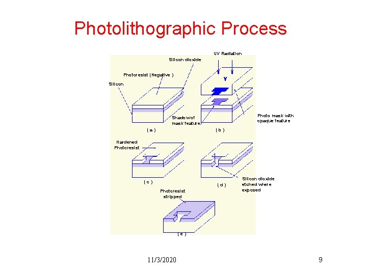
Fabrication of VLSI Circuits 1. Create 2. Define 3. Etch Silicon wafers Material formation by deposition, diffusion or implantation Pattern definition by photolithography Etch 8 to 10 iterations 11/3/2020 8

Photolithographic Process UV Radiation Silicon dioxide Photoresist (Negative ) Silicon Photo mask with opaque feature Shadow of mask feature (a) (b) Hardened Photoresist (c) (d) Photoresist stripped Silicon dioxide etched where exposed (e) 11/3/2020 9

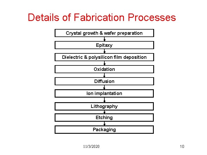
Details of Fabrication Processes Crystal growth & wafer preparation Epitaxy Dielectric & polysilicon film deposition Oxidation Diffusion Ion implantation Lithography Etching Packaging 11/3/2020 10

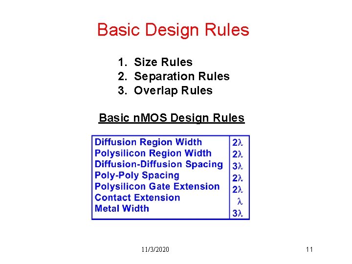
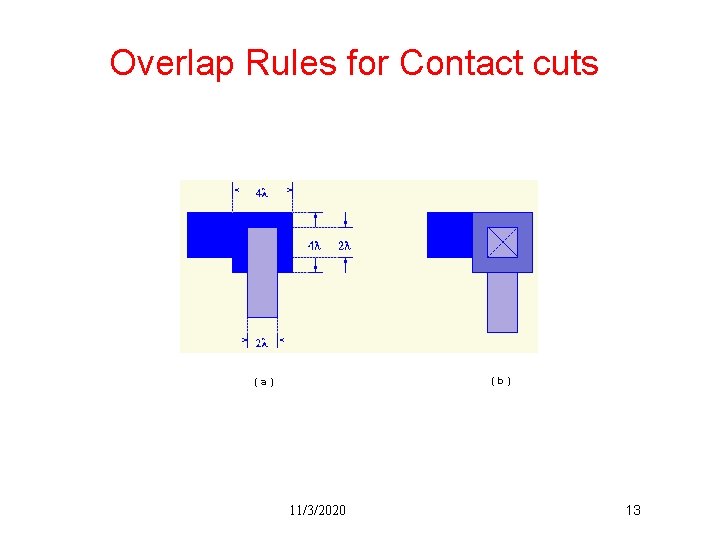
Basic Design Rules 1. Size Rules 2. Separation Rules 3. Overlap Rules Basic n. MOS Design Rules 11/3/2020 11

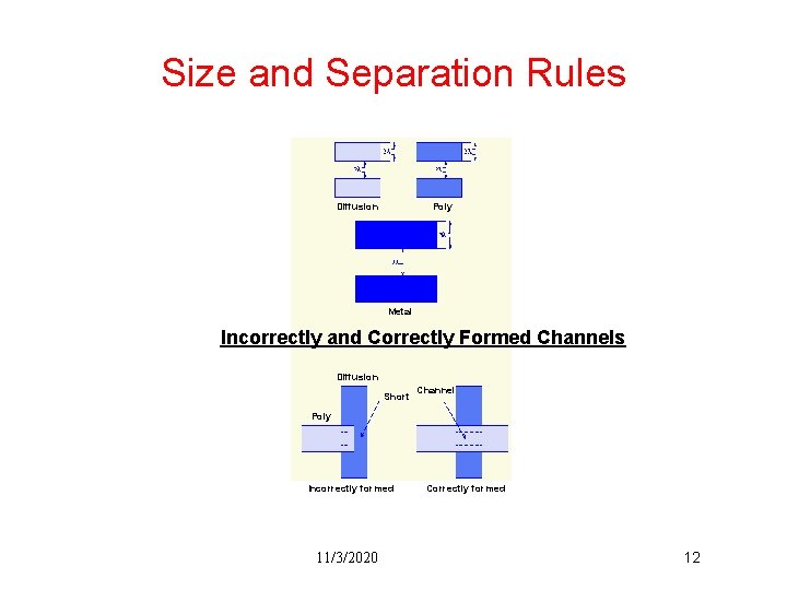
Size and Separation Rules Diffusion Poly Metal Incorrectly and Correctly Formed Channels Diffusion Short Channel Poly Incorrectly formed 11/3/2020 Correctly formed 12

Overlap Rules for Contact cuts (b) (a) 11/3/2020 13

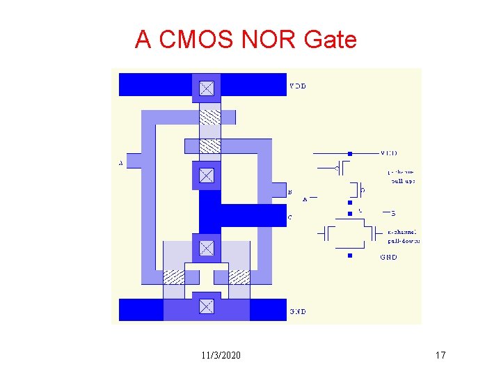
Layout of Basic Devices a n. MOS Inverter a CMOS Inverter a n. MOS NAND Gate a CMOS NAND Gate a n. MOS NOR Gate a CMOS NOR Gate Complicated devices are constructed by using basic devices 11/3/2020 14

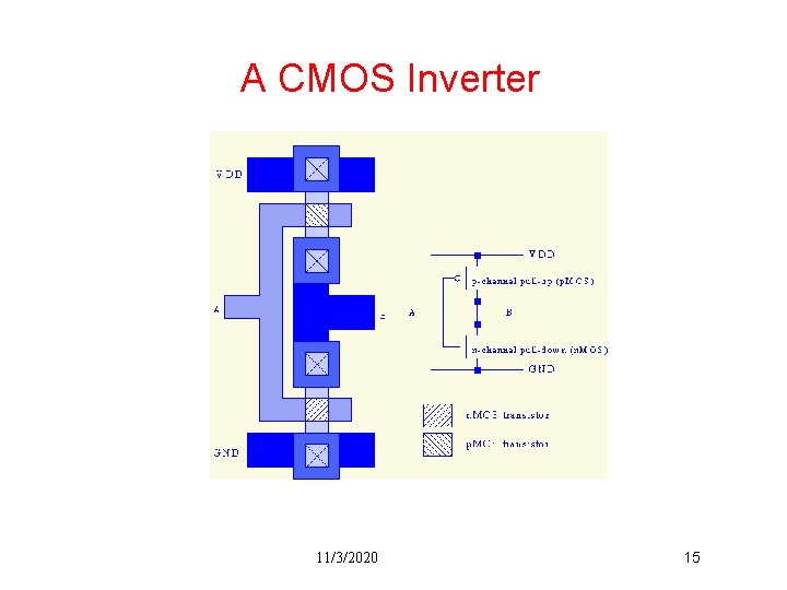
A CMOS Inverter 11/3/2020 15

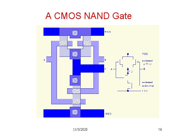
A CMOS NAND Gate 11/3/2020 16

A CMOS NOR Gate 11/3/2020 17

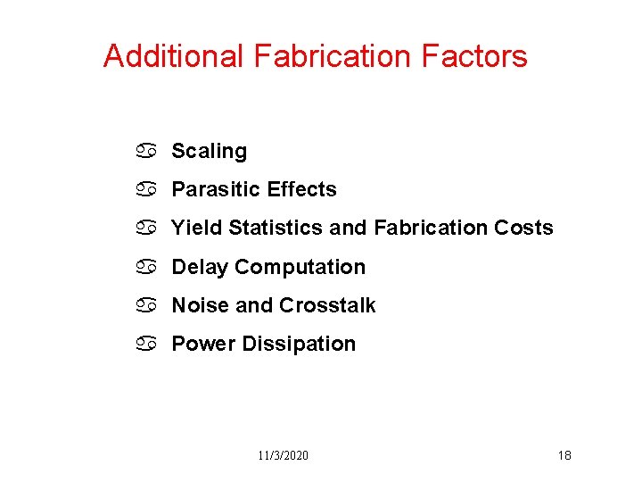
Additional Fabrication Factors a Scaling a Parasitic Effects a Yield Statistics and Fabrication Costs a Delay Computation a Noise and Crosstalk a Power Dissipation 11/3/2020 18

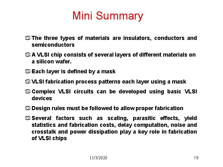
Mini Summary a The three types of materials are insulators, conductors and semiconductors a A VLSI chip consists of several layers of different materials on a silicon wafer. a Each layer is defined by a mask a VLSI fabrication process patterns each layer using a mask a Complex VLSI circuits can be developed using basic VLSI devices a Design rules must be followed to allow proper fabrication a Several factors such as scaling, parasitic effects, yield statistics and fabrication costs, delay computation, noise and crosstalk and power dissipation play a key role in fabrication of VLSI chips 11/3/2020 19

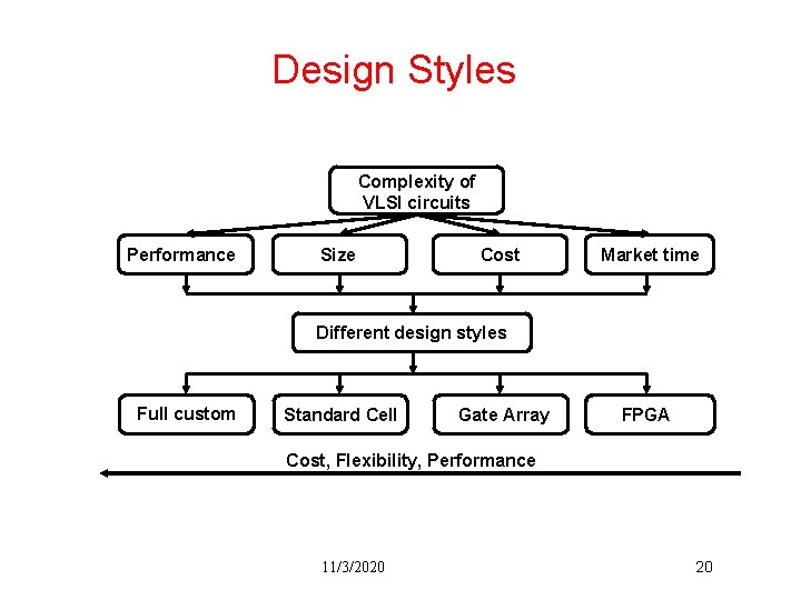
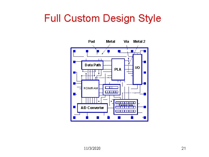
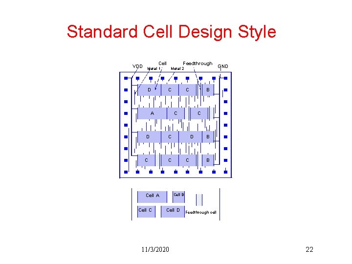
Design Styles Complexity of VLSI circuits Performance Size Cost Market time Different design styles Full custom Standard Cell Gate Array FPGA Cost, Flexibility, Performance 11/3/2020 20

Full Custom Design Style Pad Metal Via Data Path PLA Metal 2 I/O ROM/RAM A/D Converter 11/3/2020 Random logic 21

Standard Cell Design Style VDD Cell Feedthrough Metal 1 D Metal 2 C A B C D C B B Cell A Cell C C GND Cell D 11/3/2020 Feedthrough cell 22

Gate Array Design Style A C B VDD Metal 1 Metal 2 C A B 11/3/2020 23

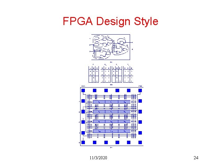
FPGA Design Style 11/3/2020 24

Field-Programmable Gate-Arrays (FPGAs) a Programmable logic a Programmable interconnects a Programmable inputs/outputs 11/3/2020 25

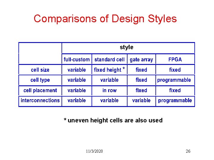
Comparisons of Design Styles style * uneven height cells are also used 11/3/2020 26

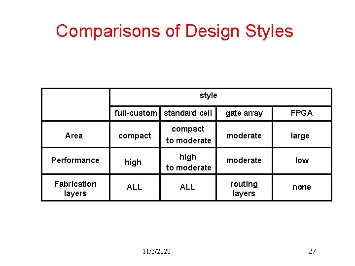
Comparisons of Design Styles style full-custom standard cell compact gate array FPGA moderate large Area compact Performance high to moderate low Fabrication layers ALL routing layers none to moderate 11/3/2020 27

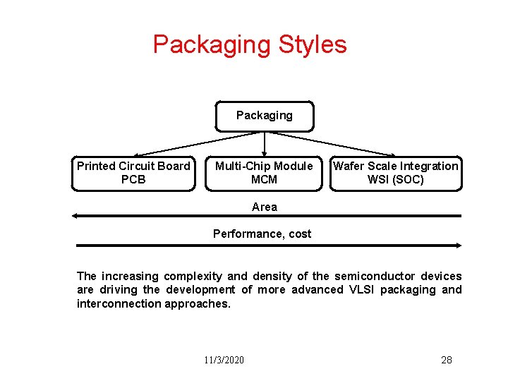
Packaging Styles Packaging Printed Circuit Board PCB Multi-Chip Module MCM Wafer Scale Integration WSI (SOC) Area Performance, cost The increasing complexity and density of the semiconductor devices are driving the development of more advanced VLSI packaging and interconnection approaches. 11/3/2020 28

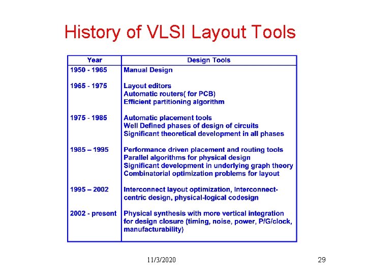
History of VLSI Layout Tools 11/3/2020 29

Now You Need Algorithms • To put devices/interconnects together into VLSI chips • Fundamental questions: How do you do it smartly? • Definition of algorithm in a board sense: A step-by-step procedure for solving a problem. Examples: – Cooking a dish – Making a phone call – Sorting a hand of cards • Definition for computational problem: A well-defined computational procedure that takes some value as input and produces some value as output 11/3/2020 30
![Example Selection Sort Input An array of n numbers D1Dn Output An Example: Selection Sort • Input: An array of n numbers D[1]…D[n]. • Output: An](https://slidetodoc.com/presentation_image/49d63b39714a60bf670700ebf26cf7ce/image-31.jpg)
Example: Selection Sort • Input: An array of n numbers D[1]…D[n]. • Output: An array of n numbers E[1]…E[n] such that E[1] E[2] … E[n]. • Algorithm: 1. For i from 1 to n do 2. Select the largest remaining no. from D[1. . n]. 3. Put that number into E[i]. 11/3/2020 31

Some Algorithm Design Techniques • • • Greedy Divide and Conquer Dynamic Programming Network Flow Mathematical Programming (e. g. , linear programming, integer linear programming) 11/3/2020 32

Reduction • Idea: If I can solve problem A, and if problem B can be transformed into an instance of problem A, then I can solve problem B by reducing problem B to problem A and then solve the corresponding problem A. • Example: – Problem A: Sorting – Problem B: Given n numbers, find the i-th largest numbers. 11/3/2020 33

Analysis of Algorithm • There can be many different algorithms to solve the same problem. • Need some way to compare 2 algorithms. • Usually run time is the most important criterion used – Space (memory) usage is of less concern now • However, difficult to compare since algorithms may be implemented in different machines, use different languages, etc. • Also, run time is input-dependent. Which input to use? • Big-O notation is widely used for asymptotic analysis 11/3/2020 34

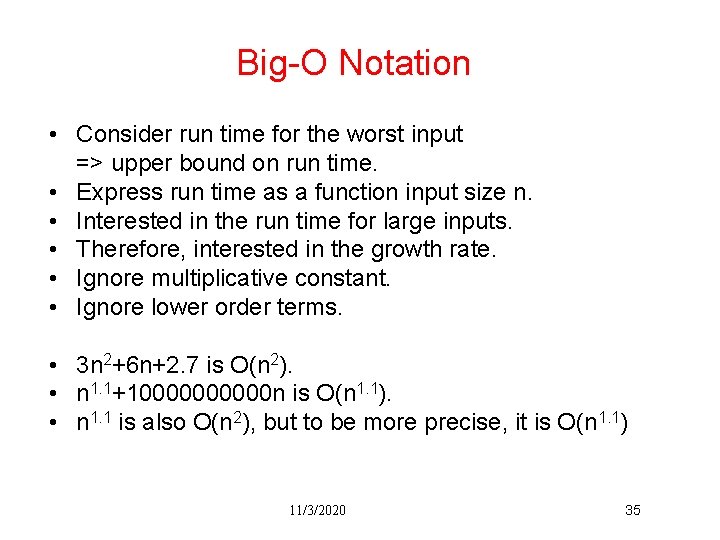
Big-O Notation • Consider run time for the worst input => upper bound on run time. • Express run time as a function input size n. • Interested in the run time for large inputs. • Therefore, interested in the growth rate. • Ignore multiplicative constant. • Ignore lower order terms. • 3 n 2+6 n+2. 7 is O(n 2). • n 1. 1+100000 n is O(n 1. 1). • n 1. 1 is also O(n 2), but to be more precise, it is O(n 1. 1) 11/3/2020 35

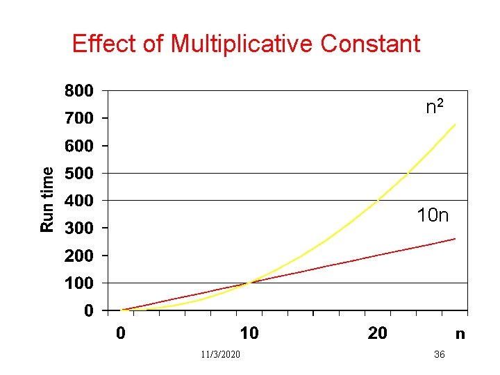
Effect of Multiplicative Constant n 2 10 n 11/3/2020 36

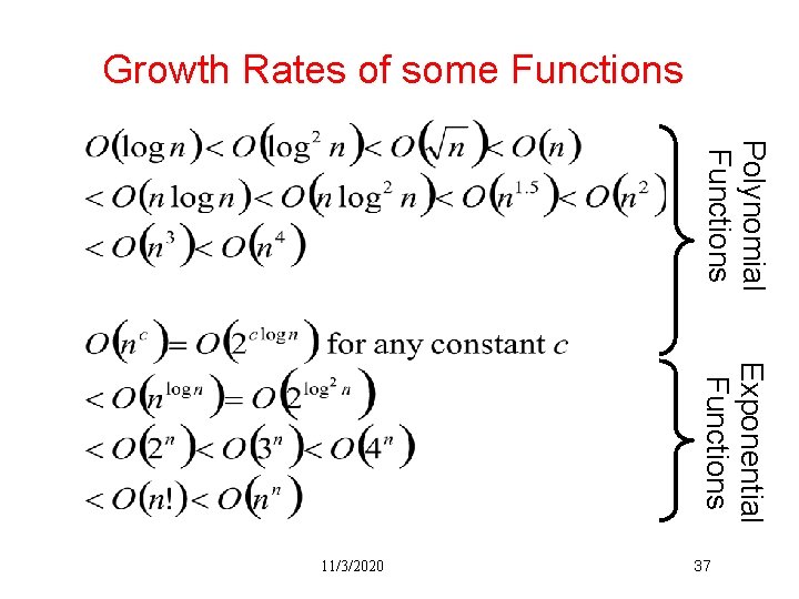
Growth Rates of some Functions Polynomial Functions Exponential Functions 11/3/2020 37

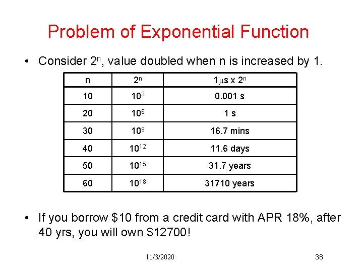
Problem of Exponential Function • Consider 2 n, value doubled when n is increased by 1. n 2 n 1 ms x 2 n 10 103 0. 001 s 20 106 1 s 30 109 16. 7 mins 40 1012 11. 6 days 50 1015 31. 7 years 60 1018 31710 years • If you borrow $10 from a credit card with APR 18%, after 40 yrs, you will own $12700! 11/3/2020 38

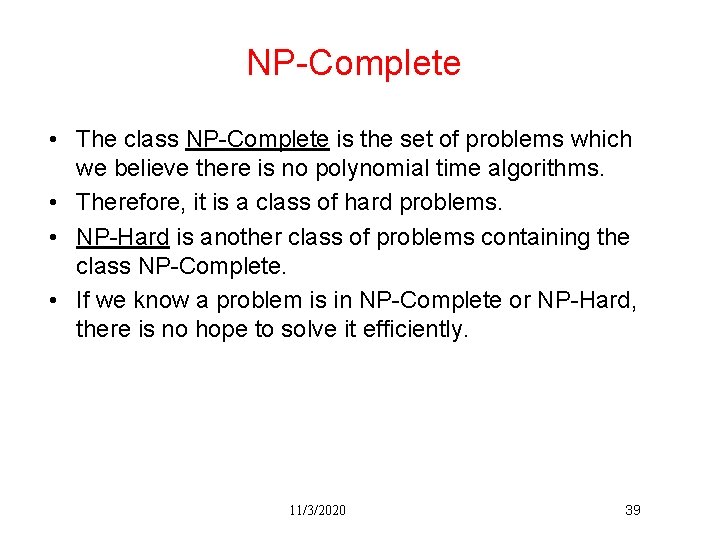
NP-Complete • The class NP-Complete is the set of problems which we believe there is no polynomial time algorithms. • Therefore, it is a class of hard problems. • NP-Hard is another class of problems containing the class NP-Complete. • If we know a problem is in NP-Complete or NP-Hard, there is no hope to solve it efficiently. 11/3/2020 39

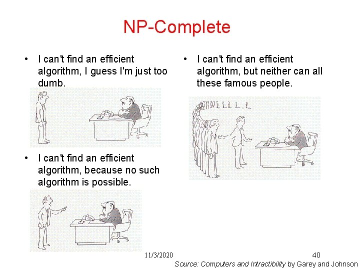
NP-Complete • I can't find an efficient algorithm, I guess I'm just too dumb. • I can't find an efficient algorithm, but neither can all these famous people. • I can't find an efficient algorithm, because no such algorithm is possible. 11/3/2020 40 Source: Computers and Intractibility by Garey and Johnson

Solution Type of Algorithms • • • Polynomial time algorithms Exponential time algorithms Special case algorithms Approximate algorithms Heuristic algorithms 11/3/2020 41

Before Next Class • Refresh your Algorithms: – C. J. Alpert, D. P. Mehta, S. S. Sapatnekar, Handbook of Algorithms for Physical Design Automation, Auerbach Publications, 2008 – T. H. Cormen, C. E. Leiserson, R. L. Rivest, C. Stein Introduction to Algorithms, MIT Press, 2009 (3 rd edition) • Circuit partitioning in the next class 11/3/2020 42