VLSI Design Lecture 3 Parasitics of CMOS Wires





- Slides: 34

VLSI Design Lecture 3: Parasitics of CMOS Wires Mohammad Arjomand CE Department Sharif Univ. of Tech. Adapted with modifications from Harris’s lecture notes

Topics Wire and via structures. n Wire parasitics. n Transistor parasitics. n Fabrication theory and practice. n Modern VLSI Design 4 e: Chapter 2 Copyright 2009 Prentice Hall PTR

Wires and vias metal 3 metal 2 vias metal 1 poly n+ p-tub Modern VLSI Design 4 e: Chapter 2 poly n+ Copyright 2009 Prentice Hall PTR

Metal interconnect n Many layers of metal interconnect are possible. – 12 layers of metal are common. Lower layers have smaller features, higher layers have larger features. n Can’t directly go from a layer to any other layer. n Modern VLSI Design 4 e: Chapter 2 Copyright 2009 Prentice Hall PTR

Copper interconnect Much better electrical characteristics. n Copper is poisonous to semiconductors--must be isolated from silicon. n – Bottom layer of interconnect is aluminum. Modern VLSI Design 4 e: Chapter 2 Copyright 2009 Prentice Hall PTR

Metal migration Current-carrying capacity of metal wire depends on cross-section. Height is fixed, so width determines current limit. n Metal migration: when current is too high, electron flow pushes around metal grains. Higher resistance increases metal migration, leading to destruction of wire. n Modern VLSI Design 4 e: Chapter 2 Copyright 2009 Prentice Hall PTR

Metal migration problems and solutions Marginal wires will fail after a small operating period—infant mortality. n Normal wires must be sized to accomodate maximum current flow: n Imax = 1. 5 m. A/ m of metal width. n Mainly applies to VDD/VSS lines. Modern VLSI Design 4 e: Chapter 2 Copyright 2009 Prentice Hall PTR

Diffusion wire capacitance n Capacitances formed by p-n junctions: sidewall capacitances depletion region n+ (ND) substrate (NA) Modern VLSI Design 4 e: Chapter 2 bottomwall capacitance Copyright 2009 Prentice Hall PTR

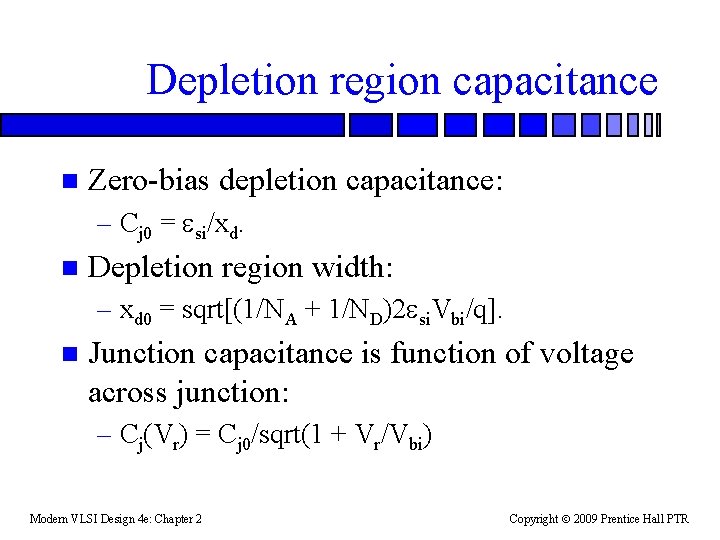
Depletion region capacitance n Zero-bias depletion capacitance: – Cj 0 = si/xd. n Depletion region width: – xd 0 = sqrt[(1/NA + 1/ND)2 si. Vbi/q]. n Junction capacitance is function of voltage across junction: – Cj(Vr) = Cj 0/sqrt(1 + Vr/Vbi) Modern VLSI Design 4 e: Chapter 2 Copyright 2009 Prentice Hall PTR

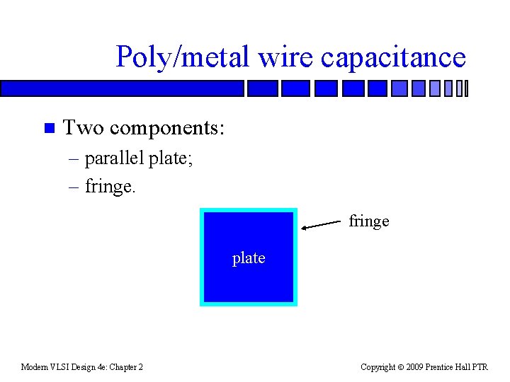
Poly/metal wire capacitance n Two components: – parallel plate; – fringe plate Modern VLSI Design 4 e: Chapter 2 Copyright 2009 Prentice Hall PTR

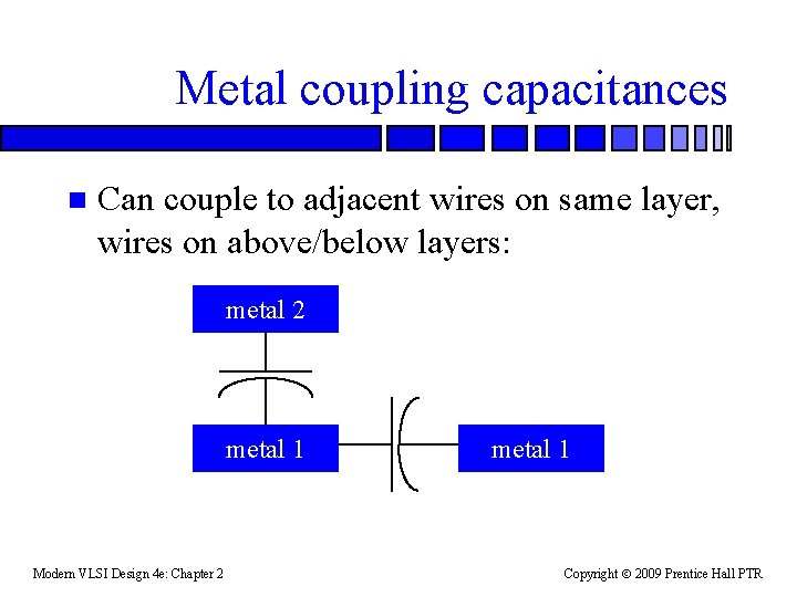
Metal coupling capacitances n Can couple to adjacent wires on same layer, wires on above/below layers: metal 2 metal 1 Modern VLSI Design 4 e: Chapter 2 metal 1 Copyright 2009 Prentice Hall PTR

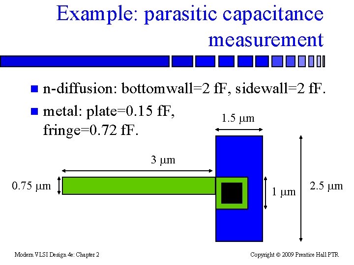
Example: parasitic capacitance measurement n-diffusion: bottomwall=2 f. F, sidewall=2 f. F. n metal: plate=0. 15 f. F, 1. 5 m fringe=0. 72 f. F. n 3 m 0. 75 m Modern VLSI Design 4 e: Chapter 2 1 m 2. 5 m Copyright 2009 Prentice Hall PTR

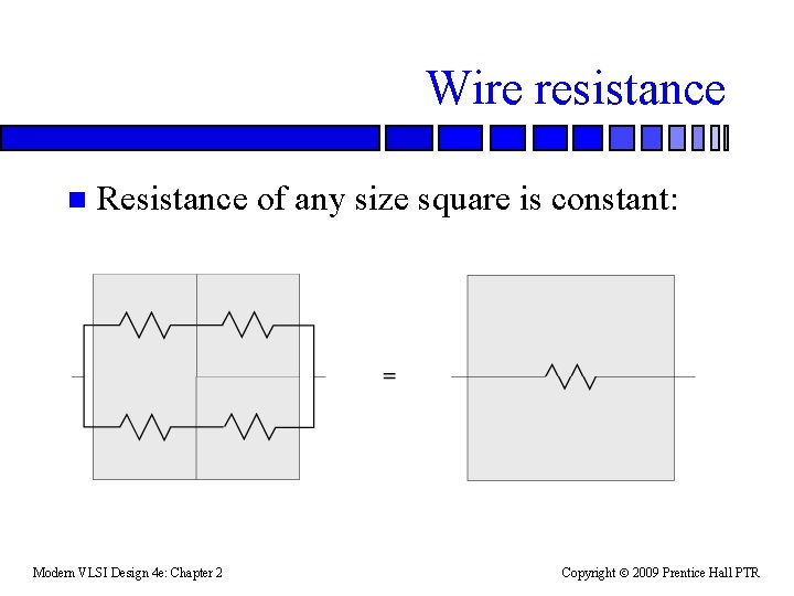
Wire resistance n Resistance of any size square is constant: Modern VLSI Design 4 e: Chapter 2 Copyright 2009 Prentice Hall PTR

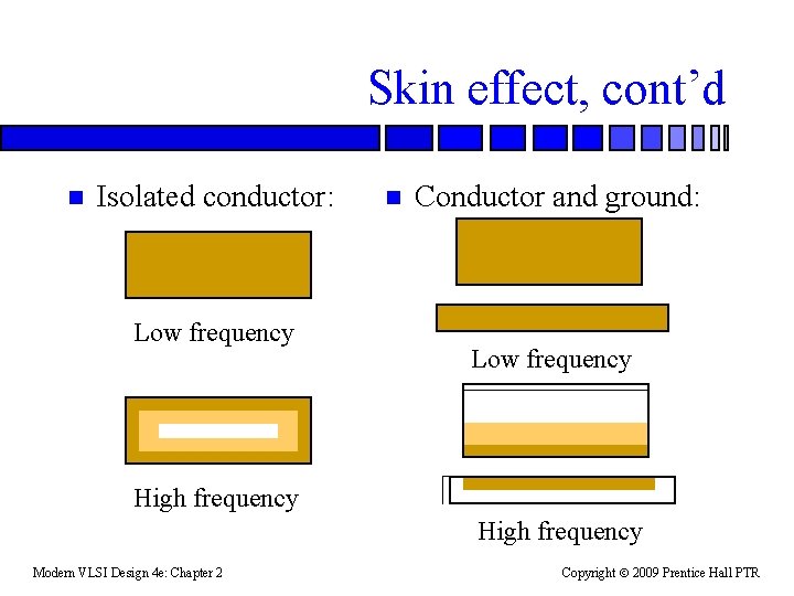
Skin effect At low frequencies, most of copper conductor’s cross section carries current. n As frequency increases, current moves to skin of conductor. n – Back EMF induces counter-current in body of conductor. n Skin effect most important at gigahertz frequencies. Modern VLSI Design 4 e: Chapter 2 Copyright 2009 Prentice Hall PTR

Skin effect, cont’d n Isolated conductor: Low frequency n Conductor and ground: Low frequency High frequency Modern VLSI Design 4 e: Chapter 2 Copyright 2009 Prentice Hall PTR

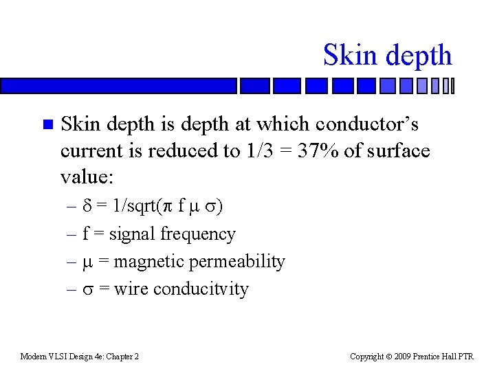
Skin depth n Skin depth is depth at which conductor’s current is reduced to 1/3 = 37% of surface value: – d = 1/sqrt(p f s) – f = signal frequency – = magnetic permeability – s = wire conducitvity Modern VLSI Design 4 e: Chapter 2 Copyright 2009 Prentice Hall PTR

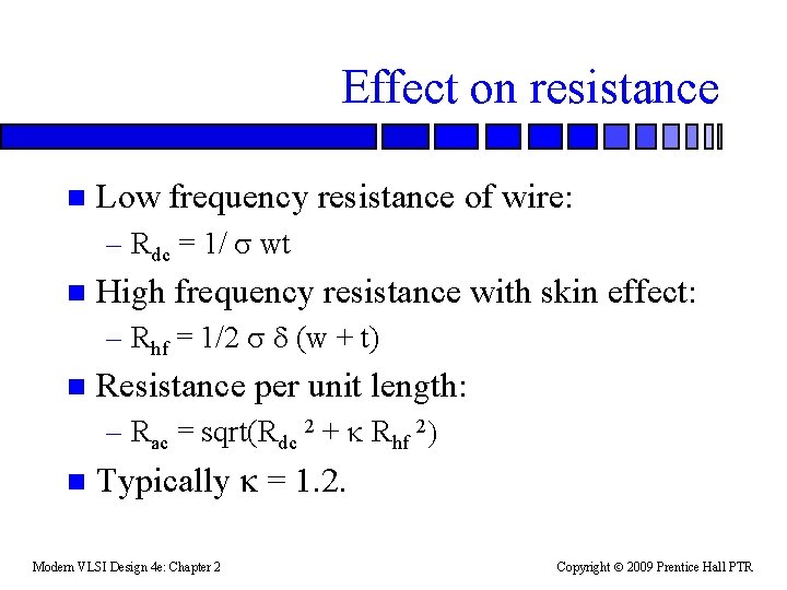
Effect on resistance n Low frequency resistance of wire: – Rdc = 1/ s wt n High frequency resistance with skin effect: – Rhf = 1/2 s d (w + t) n Resistance per unit length: – Rac = sqrt(Rdc 2 + k Rhf 2) n Typically k = 1. 2. Modern VLSI Design 4 e: Chapter 2 Copyright 2009 Prentice Hall PTR

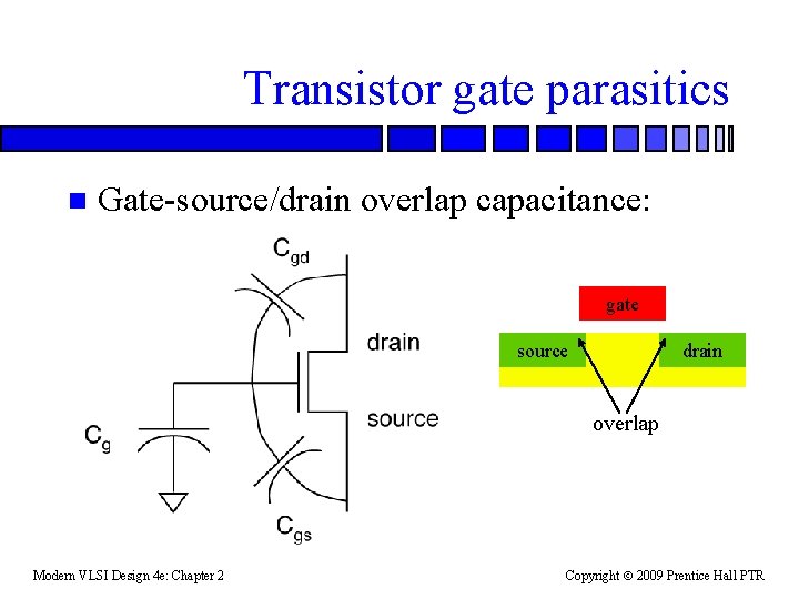
Transistor gate parasitics n Gate-source/drain overlap capacitance: gate source drain overlap Modern VLSI Design 4 e: Chapter 2 Copyright 2009 Prentice Hall PTR

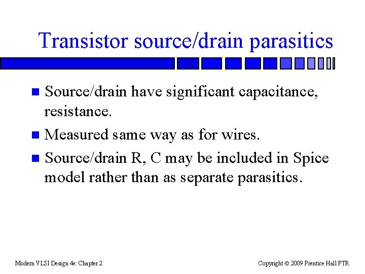
Transistor source/drain parasitics Source/drain have significant capacitance, resistance. n Measured same way as for wires. n Source/drain R, C may be included in Spice model rather than as separate parasitics. n Modern VLSI Design 4 e: Chapter 2 Copyright 2009 Prentice Hall PTR

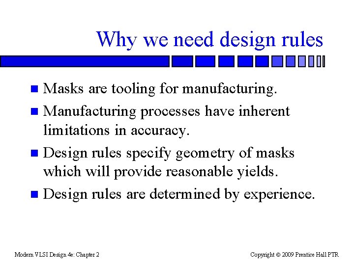
Why we need design rules Masks are tooling for manufacturing. n Manufacturing processes have inherent limitations in accuracy. n Design rules specify geometry of masks which will provide reasonable yields. n Design rules are determined by experience. n Modern VLSI Design 4 e: Chapter 2 Copyright 2009 Prentice Hall PTR

Design rules and yield Design rules are determined by manufacturing process characteristics. n Design rules should provide adequate yield if followed. n Types of design rules: n – Spacing. – Separation. – Composition. Modern VLSI Design 4 e: Chapter 2 Copyright 2009 Prentice Hall PTR

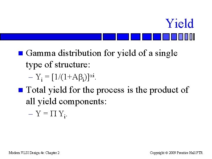
Yield n Gamma distribution for yield of a single type of structure: – Yi = [1/(1+Abi)]ai. n Total yield for the process is the product of all yield components: – Y = P Yi. Modern VLSI Design 4 e: Chapter 2 Copyright 2009 Prentice Hall PTR

Manufacturing problems Photoresist shrinkage, tearing. n Variations in material deposition. n Variations in temperature. n Variations in oxide thickness. n Impurities. n Variations between lots. n Variations across a wafer. n Modern VLSI Design 4 e: Chapter 2 Copyright 2009 Prentice Hall PTR

Transistor problems n Varaiations in threshold voltage: – oxide thickness; – ion implanatation; – poly variations. Changes in source/drain diffusion overlap. n Variations in substrate. n Modern VLSI Design 4 e: Chapter 2 Copyright 2009 Prentice Hall PTR

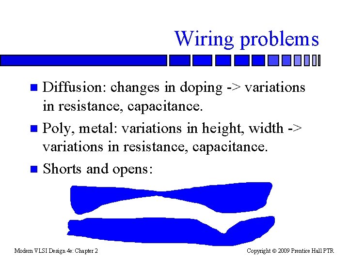
Wiring problems Diffusion: changes in doping -> variations in resistance, capacitance. n Poly, metal: variations in height, width -> variations in resistance, capacitance. n Shorts and opens: n Modern VLSI Design 4 e: Chapter 2 Copyright 2009 Prentice Hall PTR

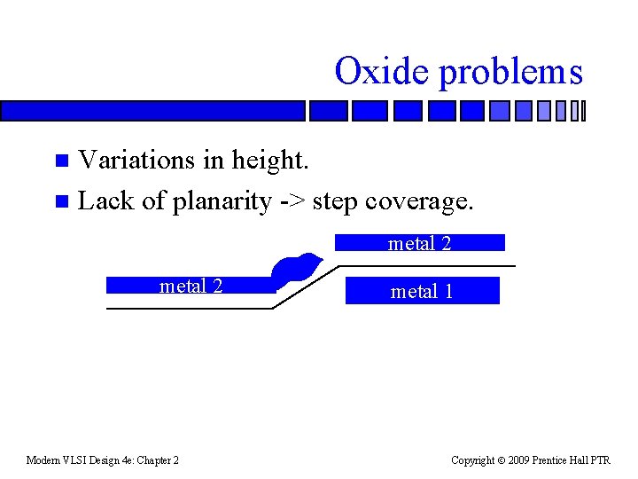
Oxide problems Variations in height. n Lack of planarity -> step coverage. n metal 2 Modern VLSI Design 4 e: Chapter 2 metal 1 Copyright 2009 Prentice Hall PTR

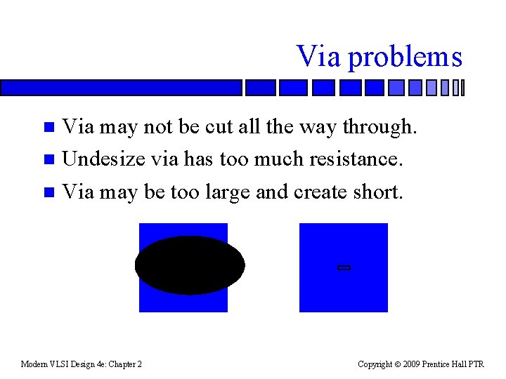
Via problems Via may not be cut all the way through. n Undesize via has too much resistance. n Via may be too large and create short. n Modern VLSI Design 4 e: Chapter 2 Copyright 2009 Prentice Hall PTR

Scaling theory n Chips get better as features shrink in classical scaling theory: – Capacitive load goes down faster than current. n Classical scaling theory runs into complications at nanometer features. – Leakage. – Smaller supply voltage. Modern VLSI Design 4 e: Chapter 2 Copyright 2009 Prentice Hall PTR

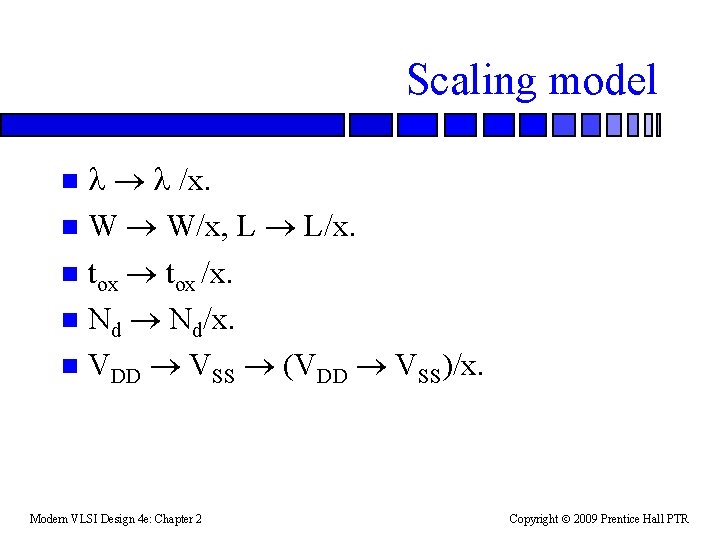
Scaling model l ® l /x. n W ® W/x, L ® L/x. n tox ® tox /x. n Nd ® Nd/x. n VDD ® VSS ® (VDD ® VSS)/x. n Modern VLSI Design 4 e: Chapter 2 Copyright 2009 Prentice Hall PTR

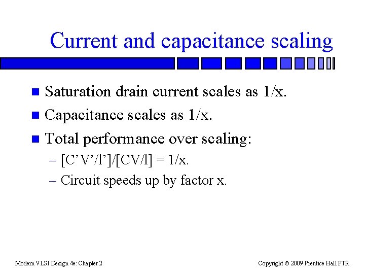
Current and capacitance scaling Saturation drain current scales as 1/x. n Capacitance scales as 1/x. n Total performance over scaling: n – [C’V’/l’]/[CV/l] = 1/x. – Circuit speeds up by factor x. Modern VLSI Design 4 e: Chapter 2 Copyright 2009 Prentice Hall PTR

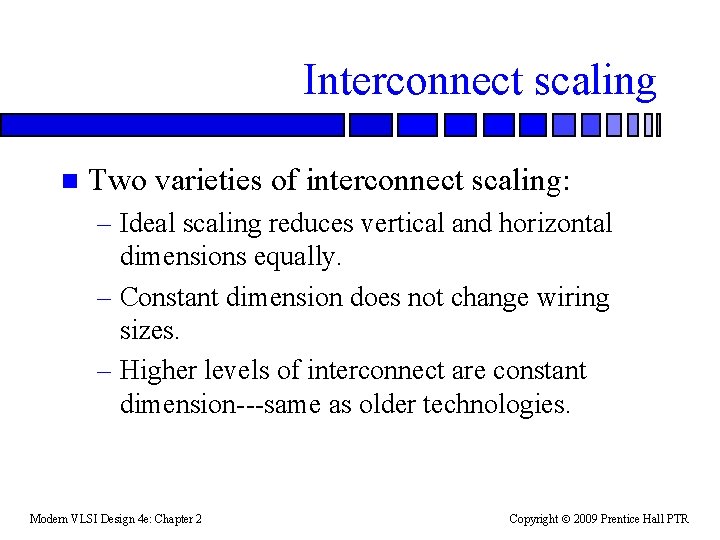
Interconnect scaling n Two varieties of interconnect scaling: – Ideal scaling reduces vertical and horizontal dimensions equally. – Constant dimension does not change wiring sizes. – Higher levels of interconnect are constant dimension---same as older technologies. Modern VLSI Design 4 e: Chapter 2 Copyright 2009 Prentice Hall PTR

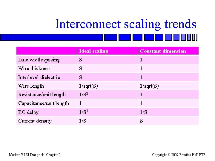
Interconnect scaling trends Ideal scaling Constant dimension Line width/spacing S 1 Wire thickness S 1 Interlevel dielectric S 1 Wire length 1/sqrt(S) Resistance/unit length 1/S 2 1 Capacitance/unit length 1 1 RC delay 1/S 3 1/S Current density 1/S S Modern VLSI Design 4 e: Chapter 2 Copyright 2009 Prentice Hall PTR

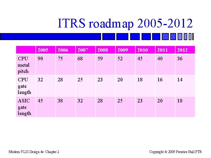
ITRS roadmap n Semiconductor industry projects fabrication trends. – Helps plan future technologies. n Roadmap describes features, technology required to get to those goals. Modern VLSI Design 4 e: Chapter 2 Copyright 2009 Prentice Hall PTR

ITRS roadmap 2005 -2012 2005 2006 2007 2008 2009 2010 2011 2012 CPU metal pitch 90 75 68 59 52 45 40 36 CPU gate length 32 28 25 23 20 18 16 14 ASIC gate length 45 38 32 28 25 23 20 18 Modern VLSI Design 4 e: Chapter 2 Copyright 2009 Prentice Hall PTR