VLSI DESIGN FLOW Introduction What is VLSI VLSI

- Slides: 21

VLSI DESIGN FLOW

Introduction What is VLSI? VLSI (very large-scale integration) is the current level of computer microchip miniaturization and refers to microchips containing in the hundreds of thousands of transistor s. LSI (large-scale integration) meant microchips containing thousands of transistors. What is the Use of VLSI? VLSI APPLICATION. VLSI stands for Very Large Scale Integration. It's used in creating so many chips and circuits on a single mini chip of silicon.

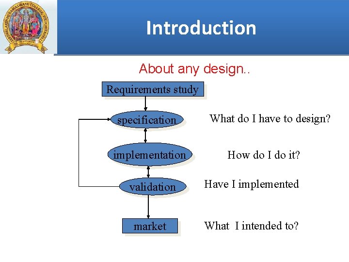
Introduction About any design. . Requirements study specification implementation What do I have to design? How do I do it? validation Have I implemented market What I intended to?

VLSI Design cycle: VLSI design cycle start with a formal specification of a VLSI chip, follows a series of steps, and eventually produces a packaged chip. VLSI SYSTEM DESIGN FLOW V. ANURADHA

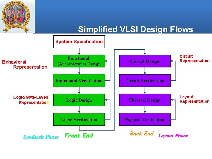
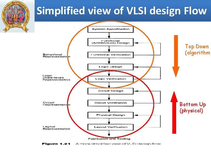
Simplified VLSI Design Flows System Specification Behavioral Representation Functional (Architecture) Design Circuit Design Functional Verification Circuit Verification Logic Design Physical Design Logic Verification Physical Verification Logic(Gate-Level) Representation Synthesis Phase Front End Circuit Representation Layout Representation Back End Layout Phase

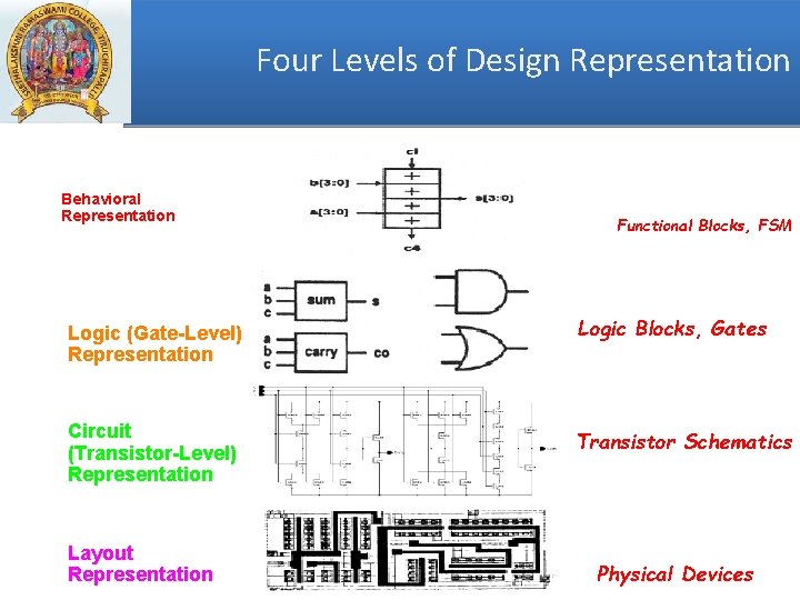
Four Levels of Design Representation Behavioral Representation Functional Blocks, FSM Logic (Gate-Level) Representation Logic Blocks, Gates Circuit (Transistor-Level) Representation Transistor Schematics Layout Representation VLSI SYSTEM DESIGN FLOW V. ANURADHA Physical Devices

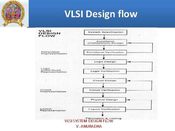
VLSI Design flow VLSI SYSTEM DESIGN FLOW V. ANURADHA

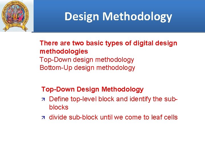
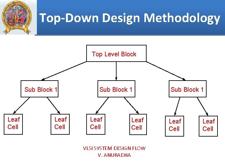
Design Methodology There are two basic types of digital design methodologies Top-Down design methodology Bottom-Up design methodology Top-Down Design Methodology ä Define top-level block and identify the subblocks ä divide sub-block until we come to leaf cells

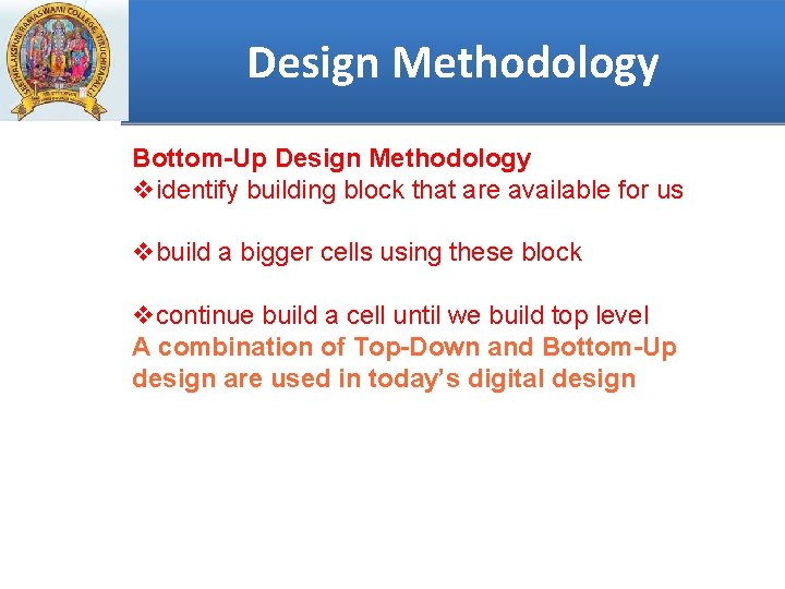
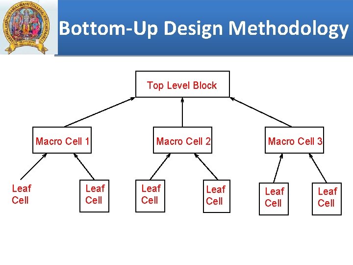
Design Methodology Bottom-Up Design Methodology videntify building block that are available for us vbuild a bigger cells using these block vcontinue build a cell until we build top level the A combination of Top-Down and Bottom-Up design are used in today’s digital design top-level

Top-Down Design Methodology Top Level Block Sub Block 1 Leaf Cell VLSI SYSTEM DESIGN FLOW V. ANURADHA Sub Block 1 Leaf Cell

Bottom-Up Design Methodology Top Level Block Macro Cell 1 Leaf Cell Macro Cell 2 Leaf Cell Macro Cell 3 Leaf Cell

Simplified view of VLSI design Flow Top Down (algorithm Bottom Up (physical)

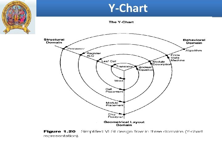
Y-Chart

System Specification v First step of design process is to lay down the specification of the system. v High level representation of the system. v Factors considered: v Performance, Functionality, Physical dimension, Design technique, Fabrication technology v It is a compromise between market requirements, technological and economical viability.

System Specification The end results are specifications of v Size, Speed, Power and Functionality of the VLSI system v Basic architecture

Functional Design v Main functional units, Interconnect requirements of the system are identified v The area, power and other parameters of each unit are estimated v The key idea is to specify behavior, in terms of Input, Output, Timing of each unit v The outcome of functional design is usually a timing diagram v This information leads to improvement of the overall design process and reduction of complexity of the subsequent phases

Logic Design the logic, that is, Boolean expressions, word width, register allocation, etc. The outcome is called an RTL (Register Transfer Level) description. RTL is expressed in a HDL (Hardware Description Language), such as VHDL and Verilog.

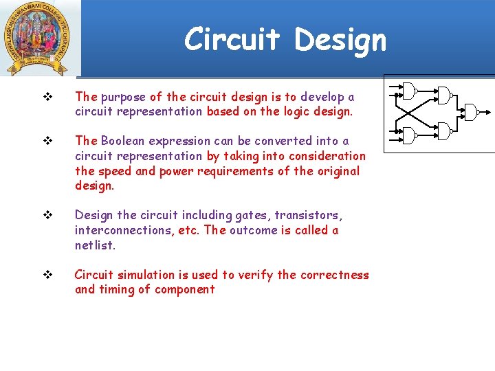
Circuit Design v The purpose of the circuit design is to develop a circuit representation based on the logic design. v The Boolean expression can be converted into a circuit representation by taking into consideration the speed and power requirements of the original design. v Design the circuit including gates, transistors, interconnections, etc. The outcome is called a netlist. v Circuit simulation is used to verify the correctness and timing of component

Physical Design Given a circuit after logic synthesis, to convert it into a layout

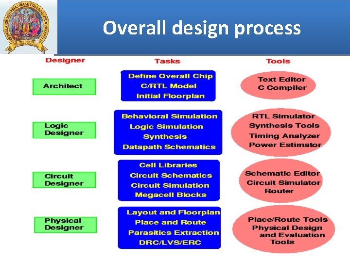
Overall design process

Thank you