VLSI CAD Overview Design Flows Algorithms and Tools
- Slides: 58

VLSI CAD Overview: Design, Flows, Algorithms and Tools Konstantin Moiseev – Intel Corp. & Technion Shmuel Wimer – Bar Ilan Univ. & Technion Compiled from various presentation from the web. Credits: David Pan – Univ. of Texas Austin Maciej Ciesielski - UMASS Andrew Kahng – UCSD Hai Zhou – Northwestern Univ. Kia Bazargan – Univ. of Minnesota Avinoam Kolodny - Technion March 2013 1

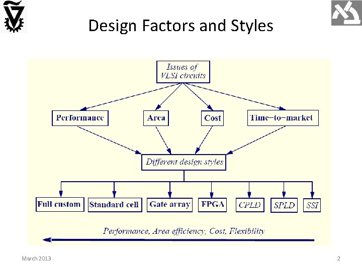
Design Factors and Styles March 2013 2

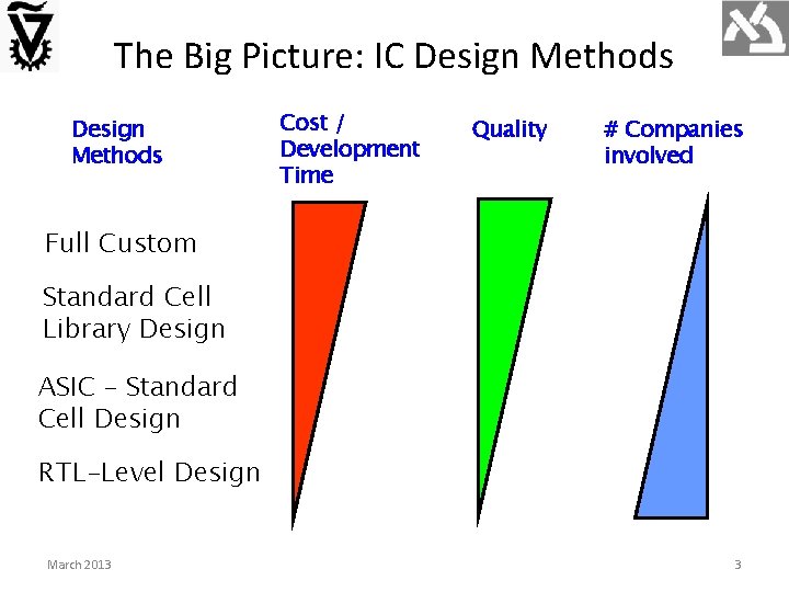
The Big Picture: IC Design Methods Cost / Development Time Quality # Companies involved Full Custom Standard Cell Library Design ASIC – Standard Cell Design RTL-Level Design March 2013 3

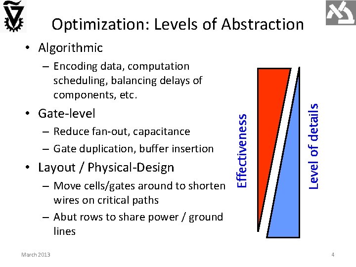
Optimization: Levels of Abstraction • Algorithmic – Reduce fan-out, capacitance – Gate duplication, buffer insertion • Layout / Physical-Design – Move cells/gates around to shorten wires on critical paths – Abut rows to share power / ground lines March 2013 Level of details • Gate-level Effectiveness – Encoding data, computation scheduling, balancing delays of components, etc. 4

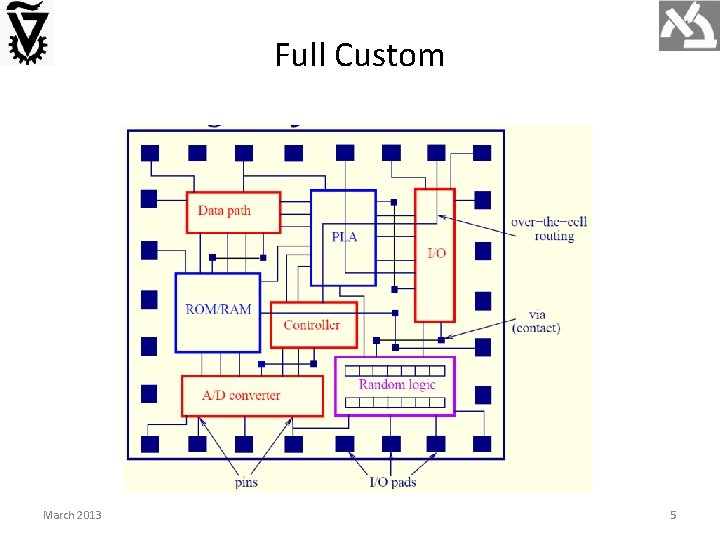
Full Custom March 2013 5

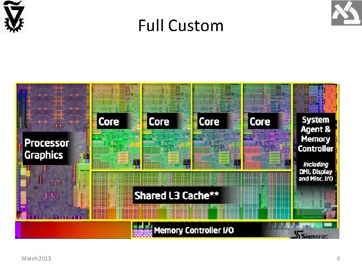
Full Custom March 2013 6

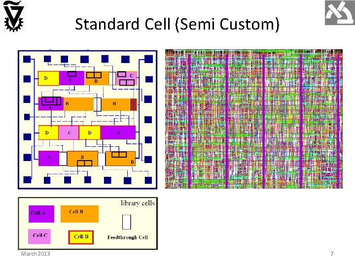
Standard Cell (Semi Custom) March 2013 7

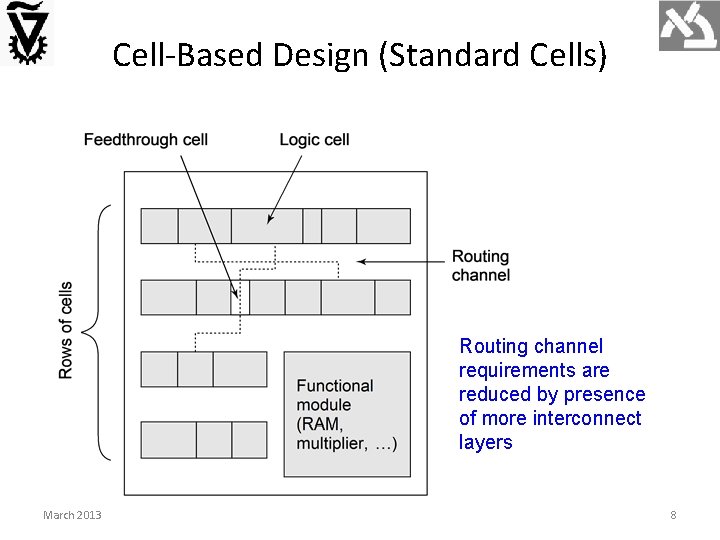
Cell-Based Design (Standard Cells) Routing channel requirements are reduced by presence of more interconnect layers March 2013 8

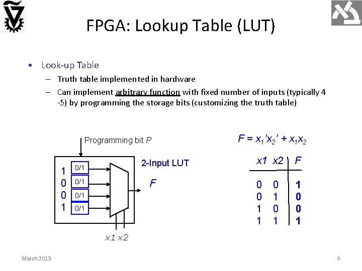
FPGA: Lookup Table (LUT) • Look-up Table – Truth table implemented in hardware – Can implement arbitrary function with fixed number of inputs (typically 4 -5) by programming the storage bits (customizing the truth table) Programming bit P 1 0 0 1 2 -Input LUT 0/1 F 0/1 0/1 F = x 1’x 2’ + x 1 x 2 x 1 x 2 F 0 0 1 1 1 0 0 1 0 1 x 2 March 2013 9

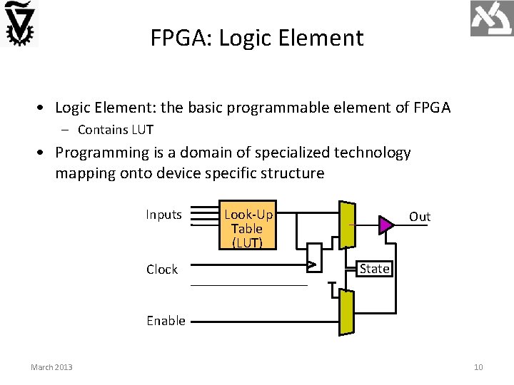
FPGA: Logic Element • Logic Element: the basic programmable element of FPGA – Contains LUT • Programming is a domain of specialized technology mapping onto device specific structure Inputs Clock Look-Up Table (LUT) Out State Enable March 2013 10

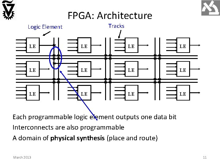
FPGA: Architecture Tracks Logic Element LE LE LE Each programmable logic element outputs one data bit Interconnects are also programmable A domain of physical synthesis (place and route) March 2013 11

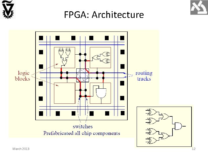
FPGA: Architecture March 2013 12

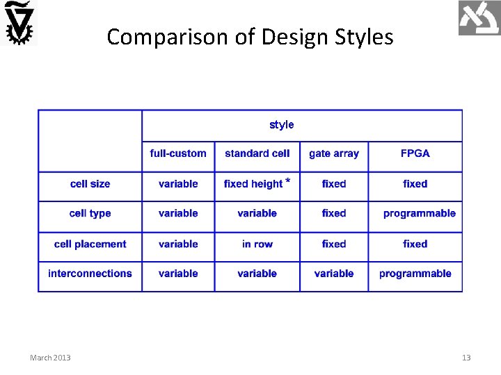
Comparison of Design Styles style March 2013 13

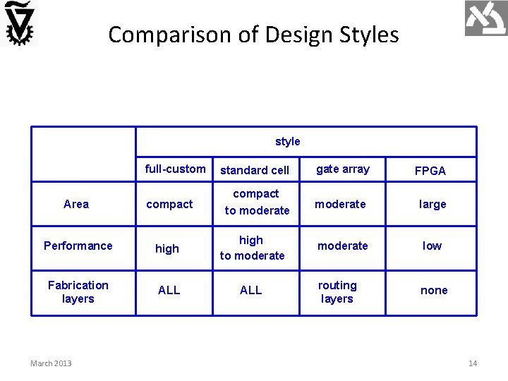
Comparison of Design Styles style full-custom standard cell compact Area compact Performance high to moderate Fabrication layers ALL March 2013 to moderate gate array FPGA moderate large moderate low routing layers none 14

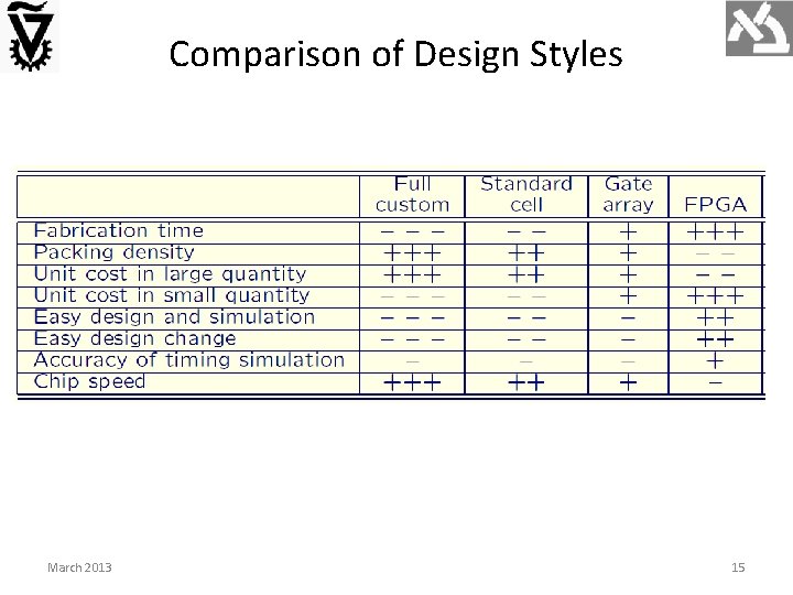
Comparison of Design Styles March 2013 15

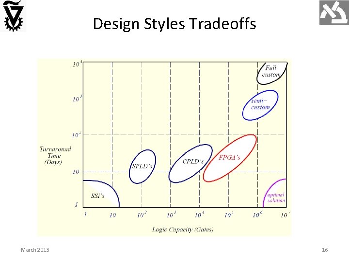
Design Styles Tradeoffs March 2013 16

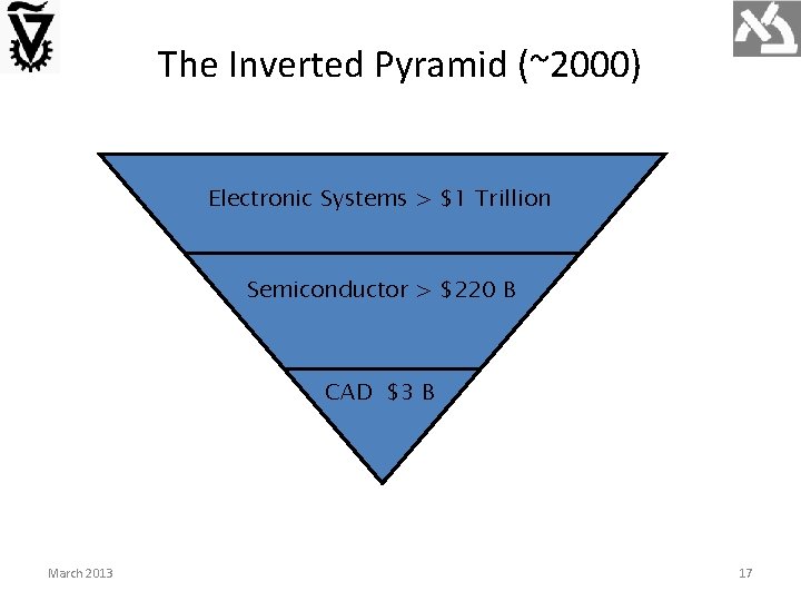
The Inverted Pyramid (~2000) Electronic Systems > $1 Trillion Semiconductor > $220 B CAD $3 B March 2013 17

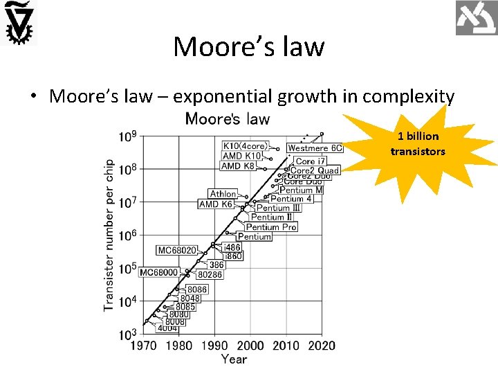
Moore’s law • Moore’s law – exponential growth in complexity 1 billion transistors

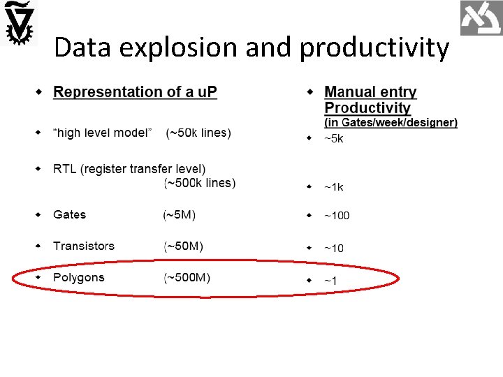
Data explosion and productivity

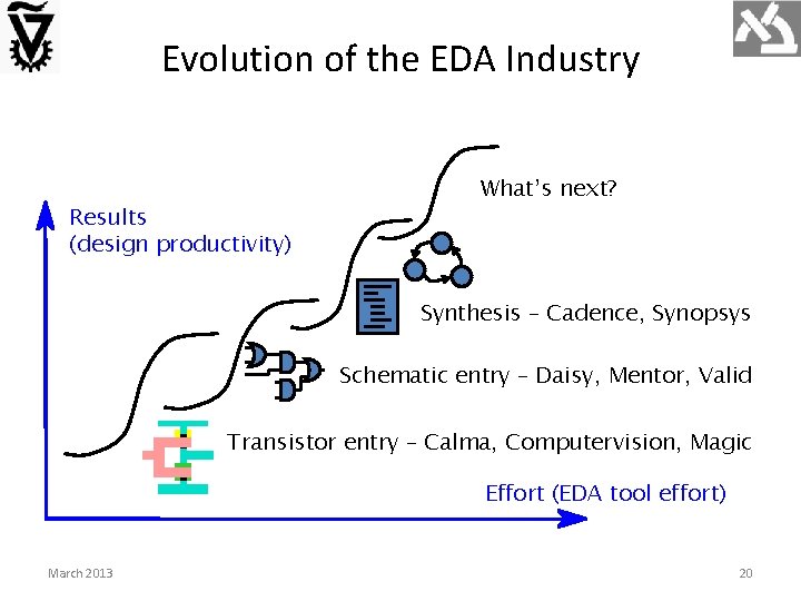
Evolution of the EDA Industry Results (design productivity) What’s next? Synthesis – Cadence, Synopsys Schematic entry – Daisy, Mentor, Valid Transistor entry – Calma, Computervision, Magic Effort (EDA tool effort) March 2013 20

History of VLSI Layout Tools March 2013 21

Synthesis and Design Process (High Level) • Application (graphics, DSP, general processor) • Algorithm (Z-buffer, FFT) • Architecture (pipeline, cash sharing, parallelism) • High level synthesis • Logic and physical synthesis March 2013 22

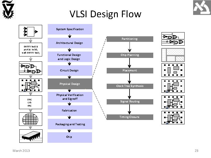
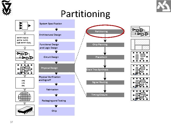
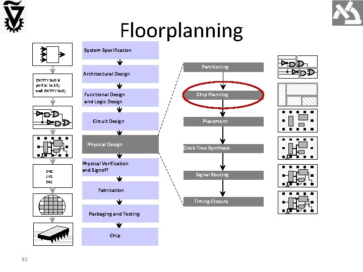
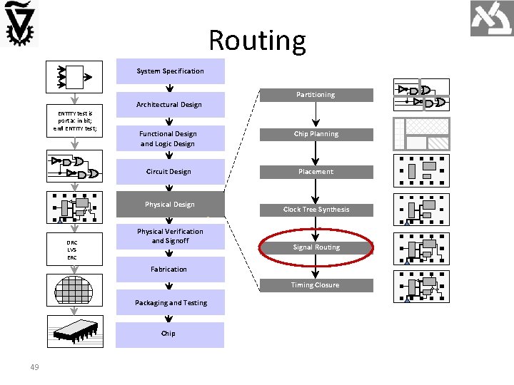
VLSI Design Flow System Specification Partitioning Architectural Design ENTITY test is port a: in bit; end ENTITY test; Functional Design and Logic Design Chip Planning Circuit Design Placement Physical Design DRC LVS ERC Physical Verification and Signoff Clock Tree Synthesis Signal Routing Fabrication Timing Closure Packaging and Testing Chip March 2013 23

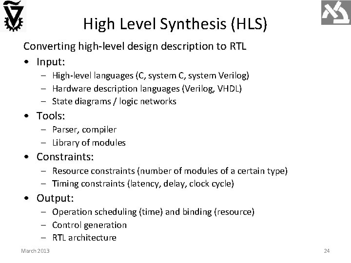
High Level Synthesis (HLS) Converting high-level design description to RTL • Input: – – – High-level languages (C, system Verilog) Hardware description languages (Verilog, VHDL) State diagrams / logic networks • Tools: – Parser, compiler – Library of modules • Constraints: – Resource constraints (number of modules of a certain type) – Timing constraints (latency, delay, clock cycle) • Output: – – – March 2013 Operation scheduling (time) and binding (resource) Control generation RTL architecture 24

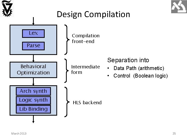
Design Compilation Lex Parse Behavioral Optimization Compilation front-end Intermediate form Separation into • Data Path (arithmetic) • Control (Boolean logic) Arch synth Logic synth Lib Binding March 2013 HLS backend 25

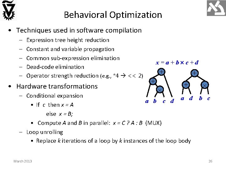
Behavioral Optimization • Techniques used in software compilation – – – Expression tree height reduction Constant and variable propagation Common sub-expression elimination Dead-code elimination Operator strength reduction (e. g. , *4 << 2) • Hardware transformations x=a+b c+d + + – Conditional expansion a b c d a d • If c then x = A else x = B; • Compute A and B in parallel: x = C ? A : B (MUX) – Loop unrolling • Replace k iterations of a loop by k instances of the loop body March 2013 b c 26

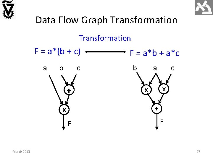
Data Flow Graph Transformation F = a*(b + c) a b c + b a c x x + x F March 2013 F = a*b + a*c F 27

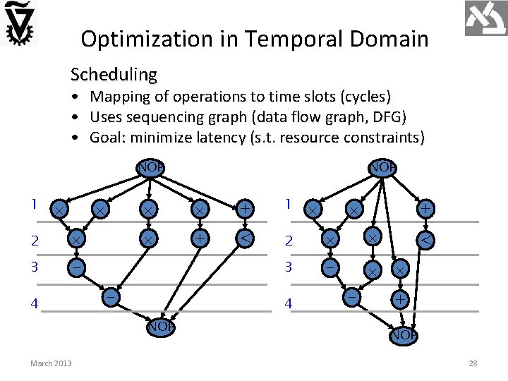
Optimization in Temporal Domain Scheduling • • • Mapping of operations to time slots (cycles) Uses sequencing graph (data flow graph, DFG) Goal: minimize latency (s. t. resource constraints) NOP 1 2 3 - 4 + 1 + < 2 3 - - 4 NOP March 2013 NOP + - < + NOP 28

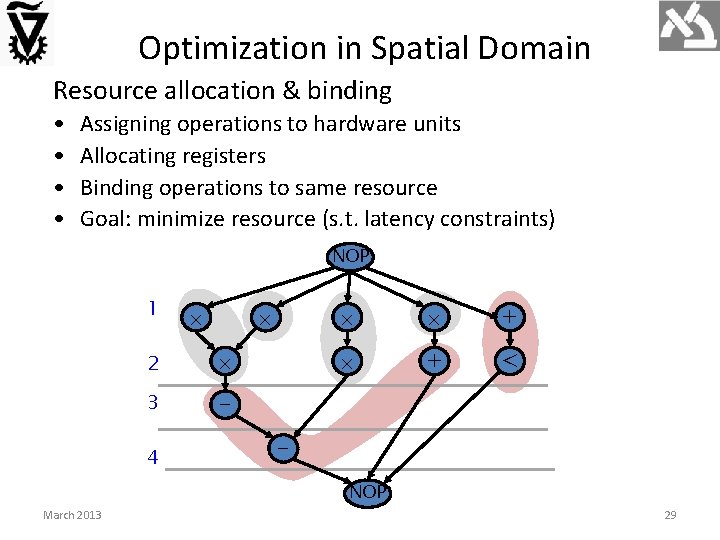
Optimization in Spatial Domain Resource allocation & binding • • Assigning operations to hardware units Allocating registers Binding operations to same resource Goal: minimize resource (s. t. latency constraints) NOP 1 2 3 - 4 + + < NOP March 2013 29

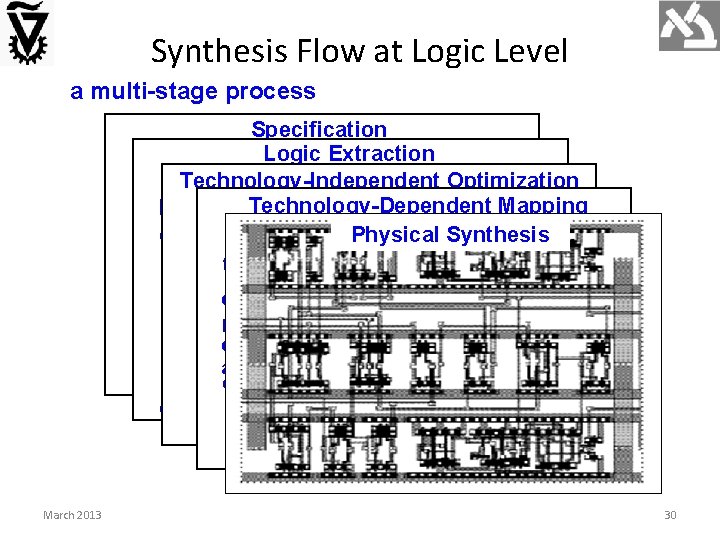
Synthesis Flow at Logic Level a multi-stage process Specification Logic Extraction module example(clk, a, b, c, d, f, g, h) Technology-Independent Optimization clk, a, b, c, d, e, f; ainput reg g, h; Mapping boutput g, a h; Technology-Dependent h begin g 1 ealways @(posedge clk)Physical 0 Synthesis G g = a | b; g 0 b f if (d) begin g if (c) h = a&~h; G h 5 else h = b; dc if (f) g = c; else a^b; h 3 b end else g H ed if (c) h = 1; else h ^b; h end a H f endmodule h 1 ce c clk d f clk March 2013 30

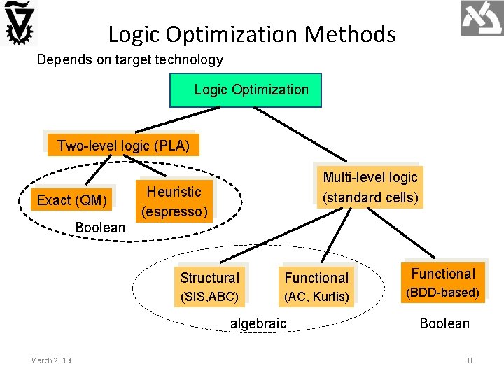
Logic Optimization Methods Depends on target technology Logic Optimization Two-level logic (PLA) Exact (QM) Multi-level logic (standard cells) Heuristic (espresso) Boolean Structural Functional (SIS, ABC) (AC, Kurtis) algebraic March 2013 Functional (BDD-based) Boolean 31

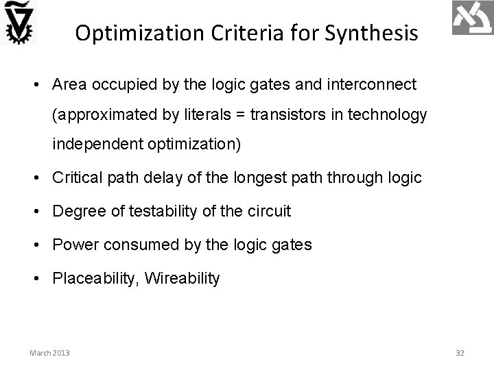
Optimization Criteria for Synthesis • Area occupied by the logic gates and interconnect (approximated by literals = transistors in technology independent optimization) • Critical path delay of the longest path through logic • Degree of testability of the circuit • Power consumed by the logic gates • Placeability, Wireability March 2013 32

Transformation-Based Synthesis sequence of transformations that change network topology and its characteristics • All modern synthesis systems are built that way – work on uniform network representation – use scripts, lists of transformations forming a strategy • Transformations are mostly algebraic – very little is based on Boolean factorization • Representation – Cube notation, BDDs, AIGs • The underlying algorithms – Algebraic transformations – Collapsing, decomposition – Factorization, substitution March 2013 33

Multi-Level Logic Minimization • Objective – Minimize number of literals – Literals represent inputs to CMOS gates • Representation – Factored form – Compatible with CMOS • Optimization techniques – Algebraic factorization and decomposition (heuristic) • Technology independent – Requires mapping onto target architecture • Standard cells • FPGAs (LUT) March 2013 34

Two-Level Logic Minimization Representation • • Truth tables Karnaugh maps Sum of Products (SOP) form Binary Decision Diagrams (BDD) Objective • Minimize number of product terms in SOP • Challenge: multiple-output functions Optimization techniques • • Quine Mc. Cluskey (optimal) Espresso logic minimizer (heuristic) Ashenhust-Curtis functional decomposition (nearly optimal) BDD-based (heuristic) March 2013 35

Physical Design Steps • • • Circuit partitioning Floorplanning Pin assignment Placement Routing Convergence March 2013 36

Partitioning System Specification Partitioning Architectural Design ENTITY test is port a: in bit; end ENTITY test; Functional Design and Logic Design Chip Planning Circuit Design Placement Physical Design DRC LVS ERC Physical Verification and Signoff Clock Tree Synthesis Signal Routing Fabrication Timing Closure Packaging and Testing Chip 37

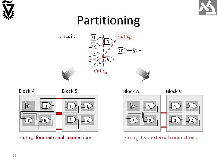
Partitioning Circuit: 1 2 3 4 5 Cut cb 7 8 6 Cut ca Block A 8 7 Block B Block A 3 4 1 6 5 2 Cut ca: four external connections 38 8 7 Block B 5 4 1 6 3 2 Cut cb: two external connections

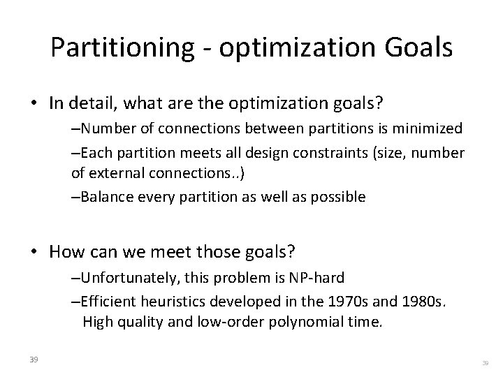
Partitioning - optimization Goals • In detail, what are the optimization goals? –Number of connections between partitions is minimized –Each partition meets all design constraints (size, number of external connections. . ) –Balance every partition as well as possible • How can we meet those goals? –Unfortunately, this problem is NP-hard –Efficient heuristics developed in the 1970 s and 1980 s. High quality and low-order polynomial time. 39 39

Floorplanning System Specification Partitioning Architectural Design ENTITY test is port a: in bit; end ENTITY test; Functional Design and Logic Design Chip Planning Circuit Design Placement Physical Design DRC LVS ERC Physical Verification and Signoff Clock Tree Synthesis Signal Routing Fabrication Timing Closure Packaging and Testing Chip 40

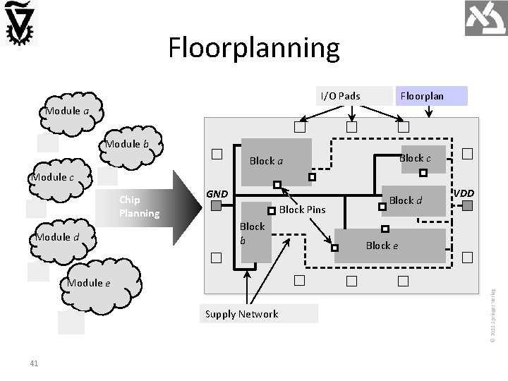
Floorplanning I/O Pads Floorplan Module a Module b Block c Block a Module c Module d GND Block Pins Block b Module e Supply Network 41 Block d VDD Block e © 2011 Springer Verlag Chip Planning

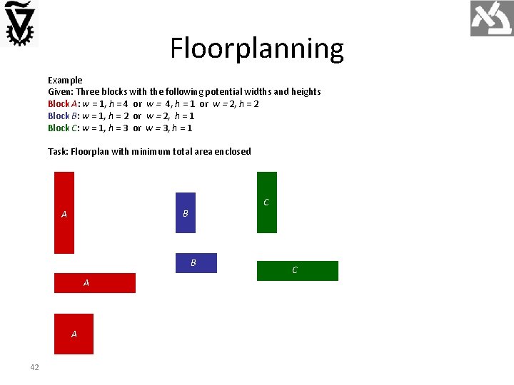
Floorplanning Example Given: Three blocks with the following potential widths and heights Block A: w = 1, h = 4 or w = 4, h = 1 or w = 2, h = 2 Block B: w = 1, h = 2 or w = 2, h = 1 Block C: w = 1, h = 3 or w = 3, h = 1 Task: Floorplan with minimum total area enclosed C B A A 42 C

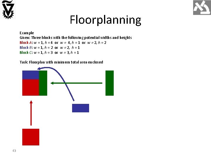
Floorplanning Example Given: Three blocks with the following potential widths and heights Block A: w = 1, h = 4 or w = 4, h = 1 or w = 2, h = 2 Block B: w = 1, h = 2 or w = 2, h = 1 Block C: w = 1, h = 3 or w = 3, h = 1 Task: Floorplan with minimum total area enclosed 43

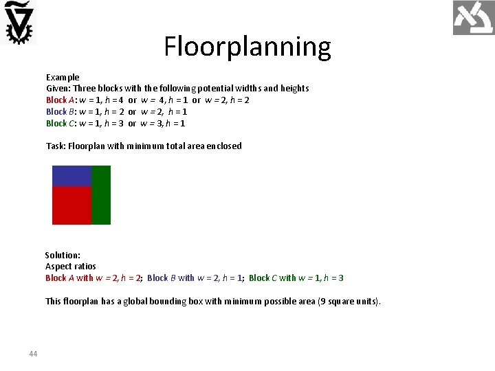
Floorplanning Example Given: Three blocks with the following potential widths and heights Block A: w = 1, h = 4 or w = 4, h = 1 or w = 2, h = 2 Block B: w = 1, h = 2 or w = 2, h = 1 Block C: w = 1, h = 3 or w = 3, h = 1 Task: Floorplan with minimum total area enclosed Solution: Aspect ratios Block A with w = 2, h = 2; Block B with w = 2, h = 1; Block C with w = 1, h = 3 This floorplan has a global bounding box with minimum possible area (9 square units). 44

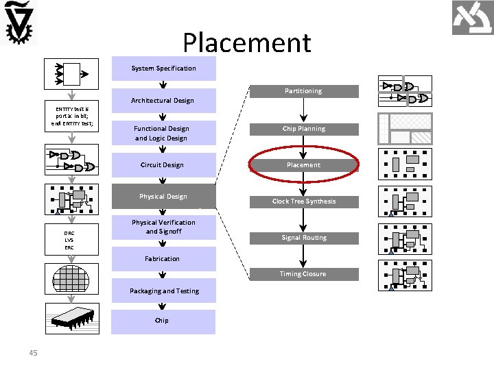
Placement System Specification Partitioning Architectural Design ENTITY test is port a: in bit; end ENTITY test; Functional Design and Logic Design Chip Planning Circuit Design Placement Physical Design DRC LVS ERC Physical Verification and Signoff Clock Tree Synthesis Signal Routing Fabrication Timing Closure Packaging and Testing Chip 45

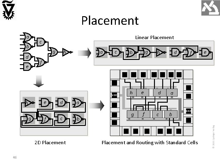
Placement b d e Linear Placement c g g f d c 2 D Placement 46 c b VDD h e g f g h d f e h a h d a a b c b GND Placement and Routing with Standard Cells © 2011 Springer Verlag a

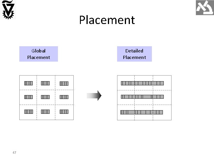
Placement Global Placement 47 Detailed Placement

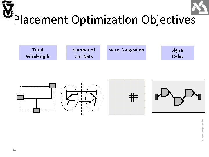
Placement Optimization Objectives Number of Cut Nets Wire Congestion Signal Delay © 2011 Springer Verlag Total Wirelength 48

Routing System Specification Partitioning Architectural Design ENTITY test is port a: in bit; end ENTITY test; Functional Design and Logic Design Chip Planning Circuit Design Placement Physical Design DRC LVS ERC Physical Verification and Signoff Clock Tree Synthesis Signal Routing Fabrication Timing Closure Packaging and Testing Chip 49

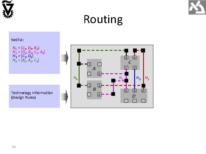
Routing Given a placement, a netlist and technology information, • determine the necessary wiring, e. g. , net topologies and specific routing segments, to connect the cells • while respecting constraints, e. g. , design rules and routing resource capacities, and • optimizing routing objectives, e. g. , minimizing total wirelength and maximizing timing slack. 50

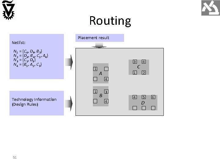
Routing Netlist: N 1 = {C 4, D 6, B 3} N 2 = {D 4, B 4, C 1, A 4} N 3 = {C 2, D 5} N 4 = {B 1, A 1, C 3} Placement result 3 1 1 Technology Information (Design Rules) 51 A B C 4 1 2 4 5 4 3 4 D 6

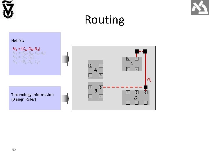
Routing Netlist: N 1 = {C 4, D 6, B 3} N 2 = {D 4, B 4, C 1, A 4} N 3 = {C 2, D 5} N 4 = {B 1, A 1, C 3} 3 1 1 Technology Information (Design Rules) 52 A B 1 C 4 2 4 N 1 3 4 4 5 D 6

Routing Netlist: N 1 = {C 4, D 6, B 3} N 2 = {D 4, B 4, C 1, A 4} N 3 = {C 2, D 5} N 4 = {B 1, A 1, C 3} 3 1 A N 4 1 Technology Information (Design Rules) 53 B 1 4 C 4 2 N 3 N 1 3 4 4 5 D 6

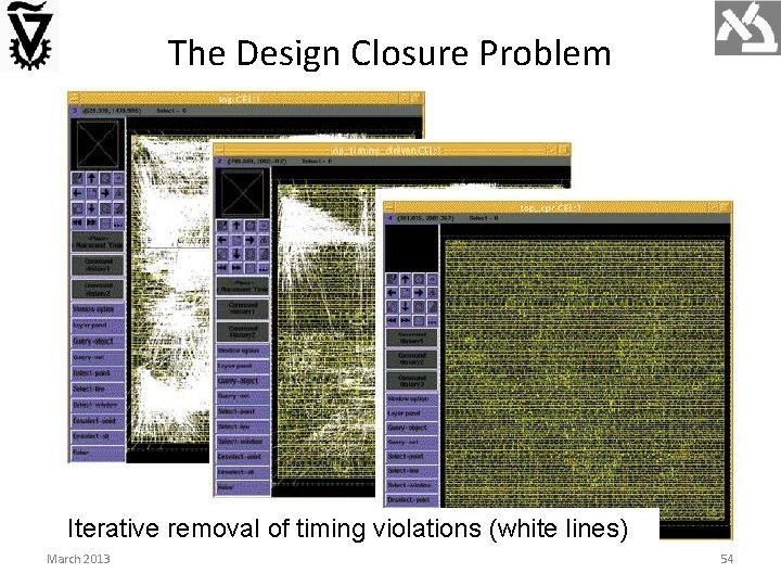
The Design Closure Problem Iterative removal of timing violations (white lines) March 2013 54

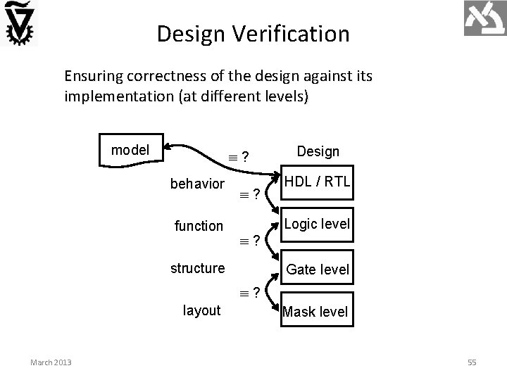
Design Verification Ensuring correctness of the design against its implementation (at different levels) model ? behavior function ? ? structure Design HDL / RTL Logic level Gate level ? layout March 2013 Mask level 55

Algorithm Design Techniques • Greedy • Divide and Conquer • Dynamic Programming • Network Flow • Mathematical Programming (e. g. , linear programming, integer linear programming) March 2013 56

Reduction • Idea: If I can solve problem A, and if problem B can be transformed into an instance of problem A, then I can solve problem B by reducing problem B to problem A and then solve the corresponding problem A. • Example: – Problem A: Sorting – Problem B: Given n numbers, find the i-th largest numbers. March 2013 57

Analysis of Algorithm • There can be many different algorithms to solve the same problem. • Need some way to compare 2 algorithms. • Usually run time is the most important criterion used – Space (memory) usage is of less concern now • However, difficult to compare since algorithms may be implemented in different machines, use different languages, etc. • Also, run time is input-dependent. Which input to use? • Big-O notation is widely used for asymptotic analysis. March 2013 58