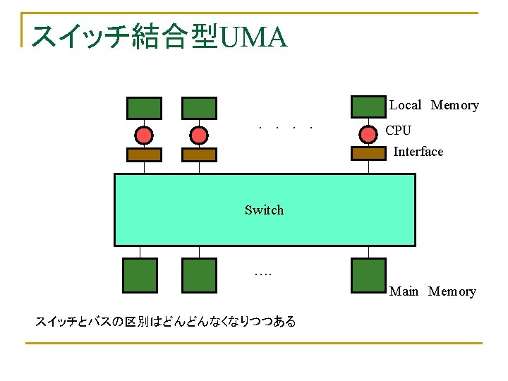
VLI Bundle128 bit Template5 bit Cycle Break 10
 group Bundle(128 bit) Template(5 bit) Cycle Break")
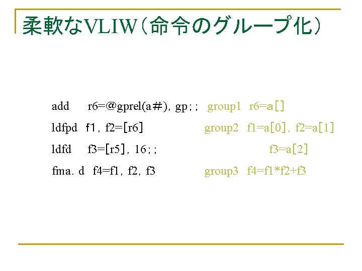
柔軟なVLIW (グループとバンドル) group Bundle(128 bit) Template(5 bit) Cycle Break

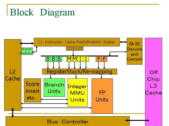
パイプライン構成 10段パイプライン、6命令同時発行 Front end Instruction Operand Delivery Execution IPG FET ROT EXP REN WLD REG EXE DET WRB IPG:Instruction Pointer generation FET:Fetch DET:Execute detect ROT:Rotate WRB:Write Back EXP:Expand REN:Rename WLD:Word-line decode REG:Register Read EXE:Execute

分岐命令の削減 predication register 1の時だけ指定されたレジスタを有効にする cmp eax,ebx jne L 30 mov ebx,CONST 1 jmp L31 L 30: mov ebx,CONST 2 L 31: cmp.eq p 7,p 8=r 14,r 15;; (p7) movi r 15=CONST 1 (p 8) movi r 16=CONST 2
![Advanced Load add r 3=4,r 0;; ld 4.a r 2=[r 33] st 4 [r 32]=r 3 add r 3=4,r](http://slidetodoc.com/presentation_image_h/d10ef1fe5fdd7341a5e49a572079d9ab/image-9.jpg "Advanced Load add r 3=4,r 0;; ld 4.a r 2=[r 33] st 4 [r 32]=r 3 add r 3=4,r")
Advanced Load add r 3=4,r 0;; ld 4.a r 2=[r 33] st 4 [r 32]=r 3 add r 3=4,r 0;; ld 4 r 2=[r 33];; st 4 [r 32]=r 3 add r 5=r 2,r 3 ld 4.c r 2=[r 33];; Advanced Load Check add r 5=r 2,r 3 st命令との間のデータ依存性は、ALAT(Advanced Load Address Table)によって解決する。

Speculative Load add 5: cmp.eq r 6,p 5=r 32,r 0;; add 5: ld 8. s r 1=[r 32] cmp. eq p 6, p 5=r 32, r 0; ; (p 6) add r 8=-1,r 0 (p 6) br.ret (p 6) add (p 5) ld 8 r 1=[r 32] (p 6) br. ret add r 8=5,r 1 (p 5) chk. s r 1, return_error br.ret;; page faultした場合、loadは待たされる r 8=-1, r 0 add r 8=5, r 1 br. ret
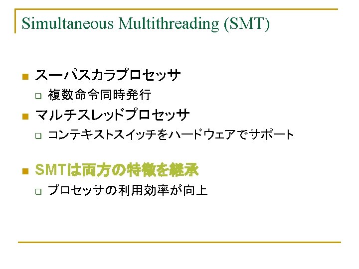

SMTの動作 Issue Slots superscalar fine-grained multithreaded superscalar SMT Clock Cycles Issue Slots
 による比較 SPECInt OS superscalar SMT 無し 有り 3. 0")
スーパスカラとの比較 Instruction Per Cycle(IPC) による比較 SPECInt OS superscalar SMT 無し 有り 3. 0 5. 9 2. 6 5. 6 Apache 無し 有り 1. 1 4. 6 SPECInt : not OS intensive application Apache : OS intensive application
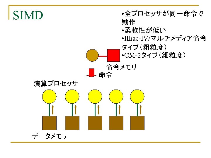
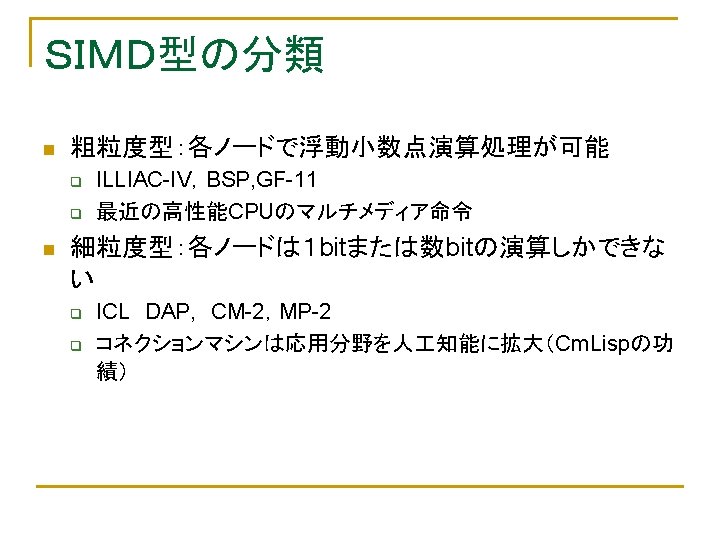
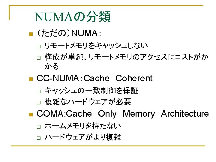
の数: M(Multiple)/S(Single) データ流(Data Stream)の数:M/S q SISD n q q q ユニプロセッサ(スーパスカラ、VLIWも入る) MISD:存在しない(Analog Computer)")
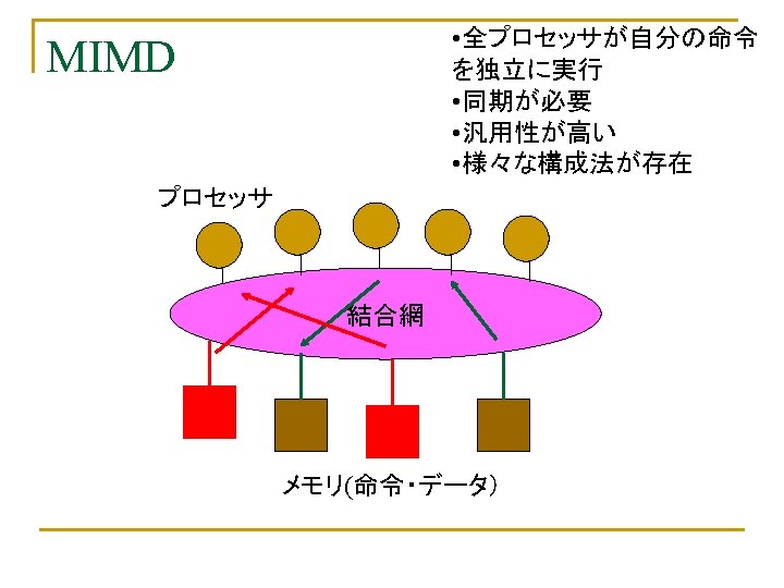
Flynnの分類 n n 命令流(Instruction Stream)の数: M(Multiple)/S(Single) データ流(Data Stream)の数:M/S q SISD n q q q ユニプロセッサ(スーパスカラ、VLIWも入る) MISD:存在しない(Analog Computer) SIMD MIMD

CM-2のプロセッサ Flags A B F OP s 256 bit memory c C Context 1 bit serial ALU

CM 2のプロセッサチップ 4096チップで 64 K PE 命令 1チップ構成 Router P P P P 4 x 4 Processor Array 12 links 4096 Hypercube connection 256 bit x 16 PE RAM
として標準部品化 オンチップに格納可能")
UMAの一例:バス結合型 Main Memory shared bus Snoop Cache PU PU SMP(Symmetric Multi. Processor)として標準部品化 オンチップに格納可能

Stanford’s Hydra Considerations in the design of Hydra CSL-TR-98 -749, CPU CPU L 1 D L1 I Cache Mem. Cont. Write Through Bus(64 b) Read/Replace Bus(256 b) On-chip L 2 Cache Off-chip L 3 Cache Int. Rambus Memory interface I/O Bus Interface Cache SRAM Array DRAM Main Memory I/O
 n n n MESI Protocol RISC+DSP Pipelined operation of bus and memory controller.")
Daytona(Lucent) n n n MESI Protocol RISC+DSP Pipelined operation of bus and memory controller. 128 bit STBus 0.25μm CMOS 4.5 m× 6 mm (small chip)
 STBus PE 0 L 1 PE 1 L 1 PE 2 L 1")
Daytona(Lucent) STBus PE 0 L 1 PE 1 L 1 PE 2 L 1 PE 3 L 1 Memory and I/O Controller semaphores arbiter
 n n n 0. 18μm copper process, 400 m㎡ 17000 M Tr.")
Power 4(IBM) n n n 0. 18μm copper process, 400 m㎡ 17000 M Tr. Inter-chip interface for MCM(Multi-Chip Module) TLP(Thread Level Parallelism) Design considering memory bandwidth Shared cache + links
 CPU 1 L 2 Shared Cache CPU 2 L 3 Tags Chip-to-Chip")
Power 4(IBM) CPU 1 L 2 Shared Cache CPU 2 L 3 Tags Chip-to-Chip Interconnect >100 GByte/s Chip-to-Chip Interconnect >500 MHz >35 GByte/s >333 MHz >10 GByte/s L 3 Cache Main Memory >500 MHz, Wave-Pipelined Expansion Buses >10 GByte/s

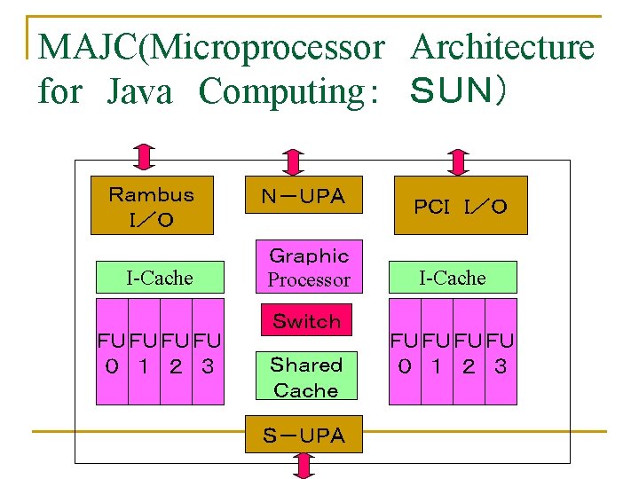
MAJC n n n Hierarchical structure Variable length VLIW processing element Shared cache I/O for inter-processor communication I/O for PCI, DRAM MAJC 5200: 0.22μm CMOS 220 mm square
 Peak 40 TFLOPS Interconnection Network (16 GB/s x 2)")
performance Earth Simulator (2002, NEC) Peak 40 TFLOPS Interconnection Network (16 GB/s x 2) Node 1 7 0 1 … Vector Processor …. Vector Processor 1 Vector Processor 0 … Shared Memory 16 GB Vector Processor 1 7 Node 0 Vector Processor … Shared Memory 16 GB Vector Processor 0 Vector Processor Shared Memory 16 GB 7 Node 639

SGI Origin Bristled Hypercube Main Memory Hub Chip Network Main MemoryはHub Chipから直接リンクを出す 2 PEで1 Cluster
 D ... ...")
DDM(Data Diffusion Machine) D ... ...
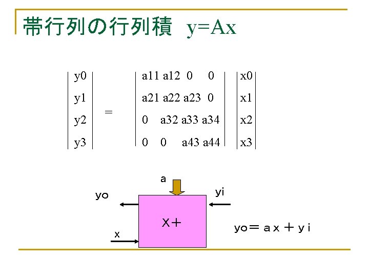

帯行列の行列積 y=Ax a 11 a 12 0 0 a 21 a 22 a 23 0 a 23 a 32 a 22 a 12 a 21 a 11 X+ x 1 0 a 32 a 33 a 34 0 0 a 43 a 44

帯行列の行列積 y=Ax a 11 a 12 0 0 a 21 a 22 a 23 0 a 33 a 23 a 32 a 22 a 12 y 1=a 11 x 1 a 21 X+ x 2 X+ x 1 0 a 32 a 33 a 34 0 0 a 43 a 44

帯行列の行列積 y=Ax a 11 a 12 0 0 a 21 a 22 a 23 0 a 34 a 43 a 33 a 23 0 a 32 a 33 a 34 0 0 a 32 a 22 y 1=a 11 x 1+ a 12 x 2 y 2=a 21 x 1 X+ x 3 x 2 x 1 a 43 a 44

帯行列の行列積 y=Ax a 11 a 12 0 a 21 a 22 a 23 0 a 44 a 34 a 43 a 33 a 23 y 2=a 21 x 1+ a 32 a 22 x 2 X+ x 3 0 X+ x 2 0 a 32 a 33 a 34 0 0 a 43 a 44

帯行列の行列積 y=Ax a 11 a 12 0 0 a 21 a 22 a 23 0 a 44 a 34 0 a 32 a 33 a 34 0 0 a 43 y 2=a 21 x 1+ a 22 x 2+ a 23 x 3 a 33 y 3= a 32 x 2 X+ x 3 x 2 a 43 a 44

 スイッチ設定 2 F.F. I/O Logic Block Switch Configuration Memory Look Up Table")
5入力テーブル SRAM型FPGA (Field Programmable Gate Array) スイッチ設定 2 F.F. I/O Logic Block Switch Configuration Memory Look Up Table
 I/O Logic Block Switch SRAM(Configuration Memory)")
SRAM型CPLD (Complex Programmable Logic Device) I/O Logic Block Switch SRAM(Configuration Memory)

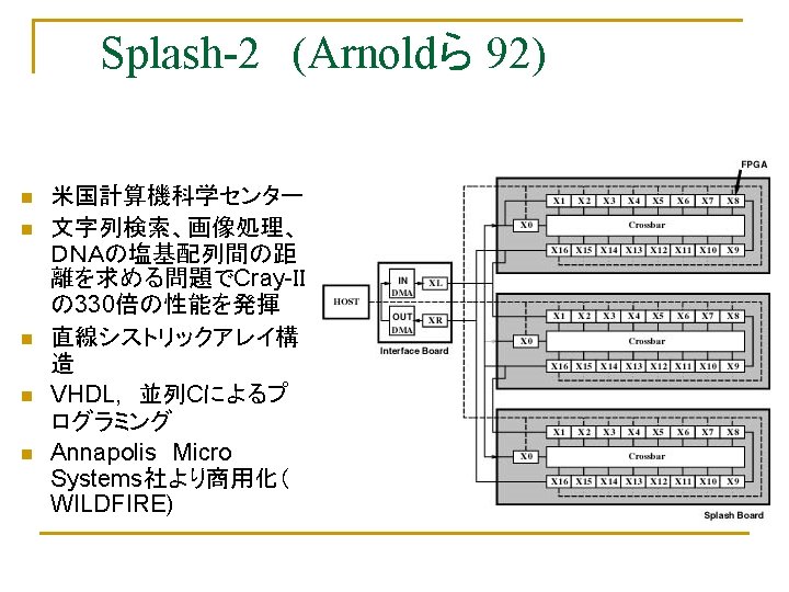
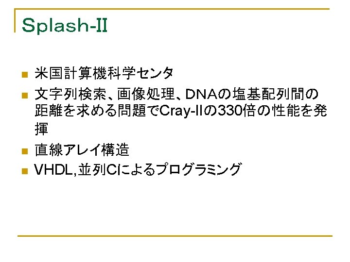
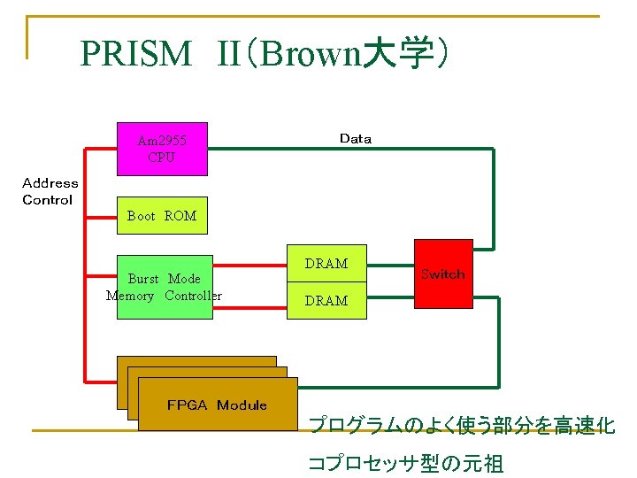
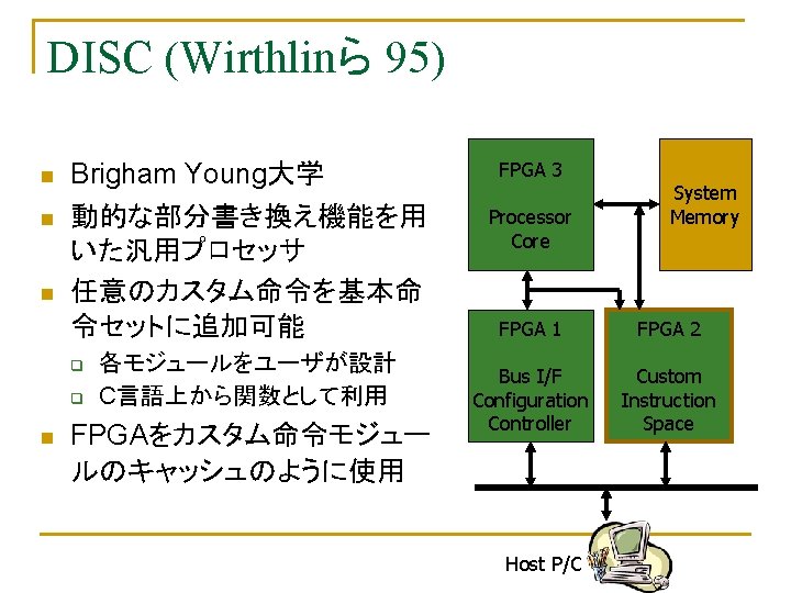
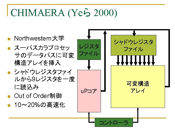
Reconfigurable Systemの発達 Stand Alone Co-processor 1990年 第 1回FPL SPLASH 1992年 第 1回Japanese SPLASH-2 FPGA/PLD Conf. RM-I 1993年 第 1回FCCM RM-III 1995年 YARDS RM-IV RM-V 2000年 PRISM-II DISC-II New Device MPLD WASMII Cache Logic Mult.Context FPGA HOSMII ATTRACTOR FIPSOC Cont.Switch.FPGA RASH Pipe. Rench PCA DRL CHIMERA Chamereon
 Compact. PCI bus CPUボード EXEボード ディスプレイ Ethernet LAN CD disk RASH unit")
RASH (三菱電機) Compact. PCI bus CPUボード EXEボード ディスプレイ Ethernet LAN CD disk RASH unit 1 Unit: 最大 6枚のEXEボードとCPUボード(Pentium) 複数のUnitを接続可能 This slide is supported by Dr. Nakajima of Mitsubishi. &p 70
 Clocks/Cont.")
EXEボードの構成 PCI-bus リンク接続とバス接続 PCI-bus I/F PCI Local-bus EXE-board controller FPGA SRAM (2 MB) Clocks/Cont. signals Local-bus FPGA 2系統のクロック PCIバスI/F SRAM搭載 DRAM付加ボード搭載可 FPGA FPGA Altera FLEX 10 K 100 A (62 K-158 KGate) &p 71
 高速シリアルリンク(1 Gbps) ATM I/O RISC FPGA RAM (LUT) ATM SW FPGA Buffer RISC")
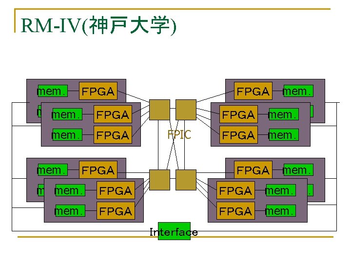
ATTRACTOR(NTT) 高速シリアルリンク(1 Gbps) ATM I/O RISC FPGA RAM (LUT) ATM SW FPGA Buffer RISC RISC Ethernet ATM通信処理に 特化したシステム MPU Mem. Compact PCI 多種類のボードを接続 ボードレベルで再構成可能
 Memory queue n n UCBのプロジェクト MIPSコアとReconfigurable Arrayが強結合しメモリ階層を 共有 コンパイラの静的解析により ループ処理を抽出しハードウ ェア化")
Garp (Hauserら 97) Memory queue n n UCBのプロジェクト MIPSコアとReconfigurable Arrayが強結合しメモリ階層を 共有 コンパイラの静的解析により ループ処理を抽出しハードウ ェア化 画像処理などでUltrasparcの 43倍の性能 MIPS Cache Q Q Q Crossbar 32 bit buses x 5 Reconfigurable Array
 n Field Programmable System Level Integrated Circuits (FPSLICs) q q 疎粒度のReconfigurable Processing Fabric、 RISC Core、PCI Controller、Memory Controller、 DMA Controller、SRAMを 1チップ上に混載 信号処理、通信プロトコル処理用、高速DSPの 5 -10 倍の性能")
Chameleon(Chameleon社) n Field Programmable System Level Integrated Circuits (FPSLICs) q q 疎粒度のReconfigurable Processing Fabric、 RISC Core、PCI Controller、Memory Controller、 DMA Controller、SRAMを 1チップ上に混載 信号処理、通信プロトコル処理用、高速DSPの 5 -10 倍の性能

Chameleon CS 2112 32 -bit PCI Bus 64 -bit Memory Bus Memory RISC Core Controller PCI Cont. 128 -bit Road. Runner Bus Configuration Subsystem DMA Subsystem Reconfigurable Processing Fabric 160 -pin Programmable I/O

CTL中の最大8命令をDPU中で 実行可能 Reconfigurable Processing Fabricの 構造 CTLは、同じサイクルで次の命 令を決定可能 LM DPU 新しいbit streamをloadする CTL LM DPU ことで構成を変えられる Tile 0 Slice 0 CTL Tile 0 Slice 3 108のDPU(Data Path Unit)が4つのSlice(各3 Tile)を構成 1 Tile: 9 DPU= 32 bit ALU X 7 16 bit + 16 bit乗算器 X 2

DPUの構成 OP:C、Verilog演算子サポート DPU単位のSIMD, パイプライン Routing MUX Instruction Register & Mask Barrel Shifter OP Register & Mask Register
- Slides: 83