Vitalis Wireless Biometric Sensor Design Review ECE 477
Vitalis Wireless Biometric Sensor Design Review ECE 477 - Spring 2013 TEAM 13 Team Members: Aakash Lamba Di Mo Shantanu Joshi Yi Shen

ECE 477 Design Review Team 13 – Fall 2013 Paste a photo of team members here, annotated with names of team members. Shantanu Joshi /Aakash Lamba / Di Mo / Yi Shen

Outline • • • Project overview Project specific success criteria Block diagram Component Selection Rationale Packaging Design Schematic and theory of operation PCB layout Software design/development status Project completion timeline Questions
Project Overview • Prototype of a portable wireless biometric sensor • Battery-powered device with fuel gauge • Mounted on the wrist • Monitor pulse rate, Sp. O 2 and skin temperature • Transmit the information via Wi-Fi for remote web access • NFC chip allows immediate access to patient data • Accelerometer on the shoulder for fall detection • Manual and automatic alarm system.
Project-Specific Success Criteria • An ability to determine pulse and Sp. O 2 readings from blood light absorption • An ability to display the users vital statistics (pulse, Sp. O 2 , skin temperature) on the LCD screen mounted on the device which is located on the patients wrist • An ability to remotely monitor the users medical status from a website via secure login or authentication through an on-device NFC tag • An ability to activate an alarm both manually (through an emergency button) and automatically in response to anomalous readings of vitals • An ability to detect if the user has suffered a fall and automatically raise an alarm
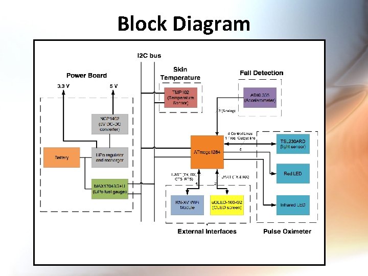
Block Diagram
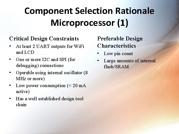
Component Selection Rationale Microprocessor (1) Critical Design Constraints • At least 2 UART outputs for Wi. Fi and LCD • One or more I 2 C and SPI (for debugging) connections • Operable using internal oscillator (8 MHz or more) • Low power consumption (< 20 m. A active) • Has a well established design tool chain Preferable Design Characteristics • Low pin count • Large amounts of internal flash/SRAM
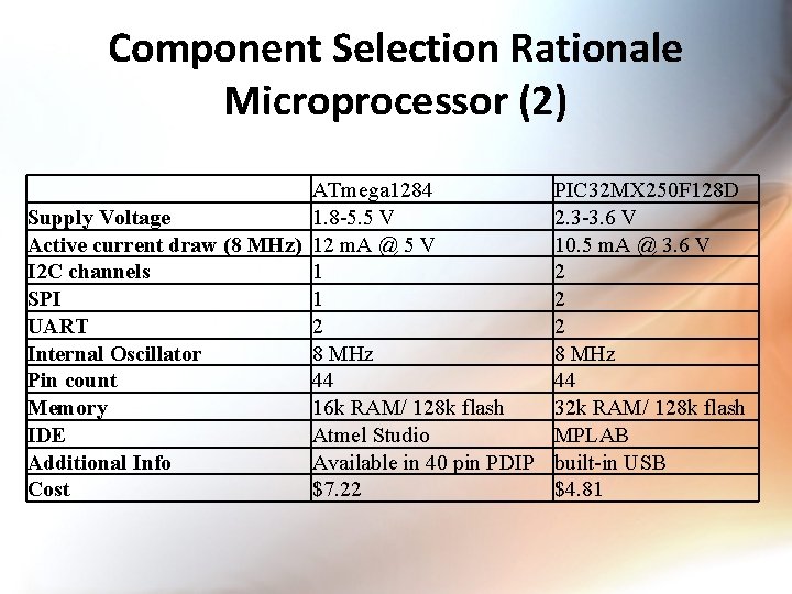
Component Selection Rationale Microprocessor (2) ATmega 1284 Supply Voltage 1. 8 -5. 5 V Active current draw (8 MHz) 12 m. A @ 5 V I 2 C channels 1 SPI 1 UART 2 Internal Oscillator 8 MHz Pin count 44 Memory 16 k RAM/ 128 k flash IDE Atmel Studio Additional Info Available in 40 pin PDIP Cost $7. 22 PIC 32 MX 250 F 128 D 2. 3 -3. 6 V 10. 5 m. A @ 3. 6 V 2 2 2 8 MHz 44 32 k RAM/ 128 k flash MPLAB built-in USB $4. 81
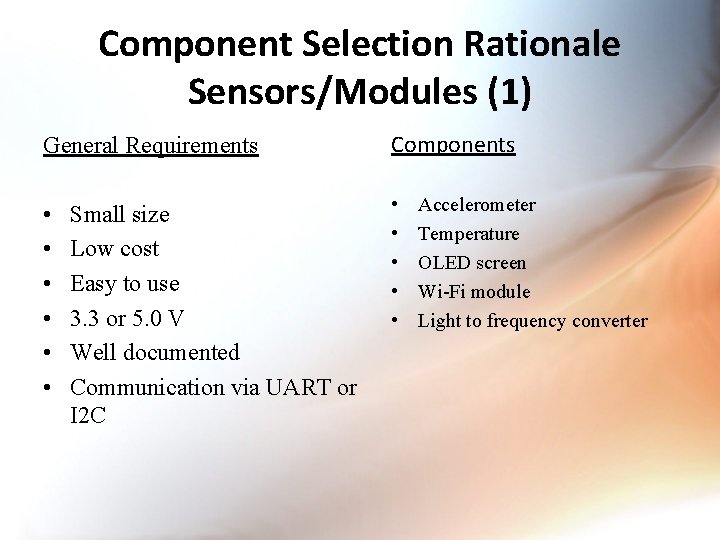
Component Selection Rationale Sensors/Modules (1) General Requirements Components • • • Small size Low cost Easy to use 3. 3 or 5. 0 V Well documented Communication via UART or I 2 C Accelerometer Temperature OLED screen Wi-Fi module Light to frequency converter
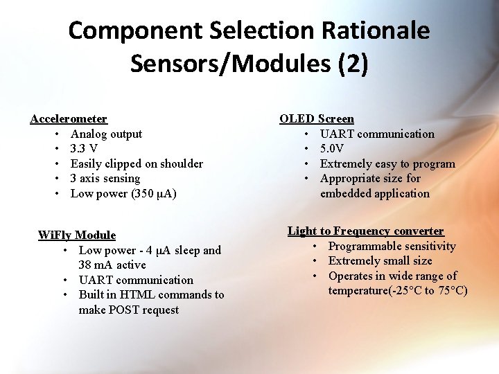
Component Selection Rationale Sensors/Modules (2) Accelerometer • Analog output • 3. 3 V • Easily clipped on shoulder • 3 axis sensing • Low power (350 μA) Wi. Fly Module • Low power - 4 μA sleep and 38 m. A active • UART communication • Built in HTML commands to make POST request OLED Screen • UART communication • 5. 0 V • Extremely easy to program • Appropriate size for embedded application Light to Frequency converter • Programmable sensitivity • Extremely small size • Operates in wide range of temperature(-25°C to 75°C)
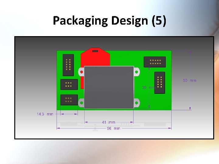
Packaging Design (1) Packaging Constraints • Portable - The device must be portable such that a patient may move around while carrying it. It should operate wirelessly so as to enable patient mobility. • Light weight – The device must be light weight. Since the average weight of a smart phone is 120 g, we are targeting something on the order of 100150 g. • Small – The device needs to be small since it needs to be mounted on to the users wrist. We are aiming to make the breadth less than 5 cm. The average wrist is approximately 4. 7 cm in diameter.
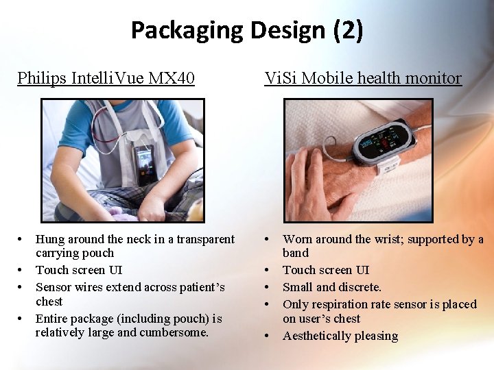
Packaging Design (2) Philips Intelli. Vue MX 40 Vi. Si Mobile health monitor • • • Hung around the neck in a transparent carrying pouch Touch screen UI Sensor wires extend across patient’s chest Entire package (including pouch) is relatively large and cumbersome. • • Worn around the wrist; supported by a band Touch screen UI Small and discrete. Only respiration rate sensor is placed on user’s chest Aesthetically pleasing
Packaging Design (3)
Packaging Design (4)
Packaging Design (5)
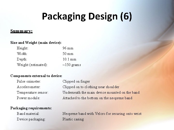
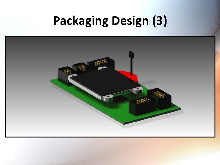
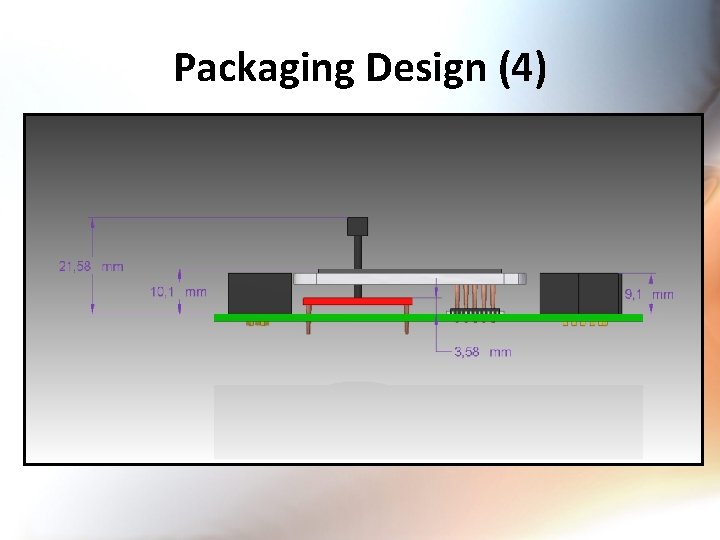
Packaging Design (6) Summary: Size and Weight (main device): Height: 96 mm Width: 50 mm Depth: 10. 1 mm Weight (estimated): ~150 grams Components external to device: Pulse oximeter: Clipped on finger Accelerometer: Clipped on to clothing near shoulder Temperature sensor: Underneath the main device mounted on the band Power module: Attached to the bottom on the neoprene band Packaging requirements: Band material: Device packaging: Neoprene band with Velcro for securing onto wrist Plastic casing
Schematic: Complete Design
Schematic: Section Breakdown Sensors External Interfaces Microcontroller Power and Battery Management
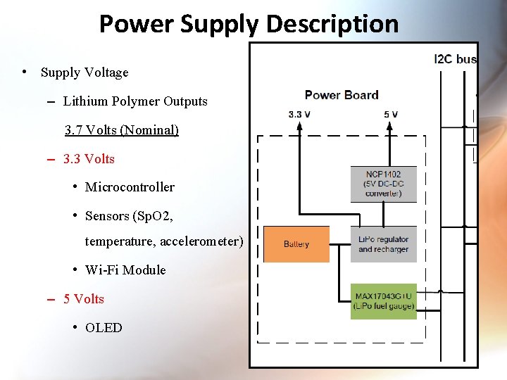
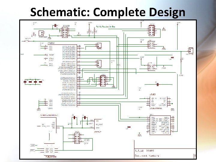
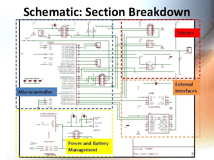
Power Supply Description • Supply Voltage – Lithium Polymer Outputs 3. 7 Volts (Nominal) – 3. 3 Volts • Microcontroller • Sensors (Sp. O 2, temperature, accelerometer) • Wi-Fi Module – 5 Volts • OLED
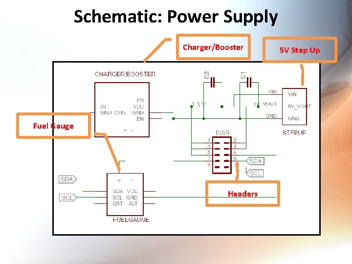
Schematic: Power Supply Charger/Booster Fuel Gauge Headers 5 V Step Up
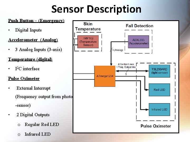
Sensor Description Push Button – (Emergency) • Digital Inputs Accelerometer (Analog) • 3 Analog Inputs (3 -axis) Temperature (digital) • I 2 C interface Pulse Oximeter • External Interrupt (Frequency output from photo -sensor) • 2 Digital Outputs o Regular Red LED o Infrared LED
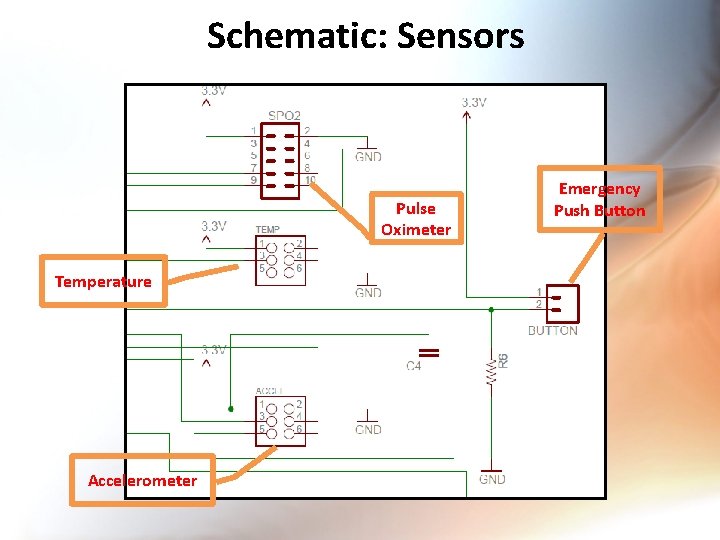
Schematic: Sensors Pulse Oximeter Temperature Accelerometer Emergency Push Button
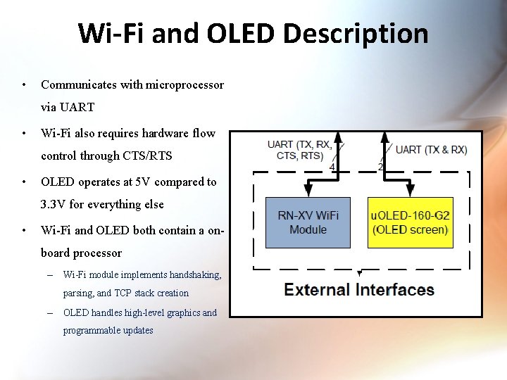
Wi-Fi and OLED Description • Communicates with microprocessor via UART • Wi-Fi also requires hardware flow control through CTS/RTS • OLED operates at 5 V compared to 3. 3 V for everything else • Wi-Fi and OLED both contain a onboard processor – Wi-Fi module implements handshaking, parsing, and TCP stack creation – OLED handles high-level graphics and programmable updates
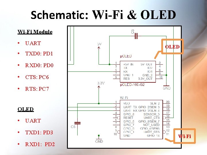
Schematic: Wi-Fi & OLED Wi-Fi Module • UART OLED • TXD 0: PD 1 • RXD 0: PD 0 • CTS: PC 6 • RTS: PC 7 OLED • UART • TXD 1: PD 3 • RXD 1: PD 2 Wi-Fi
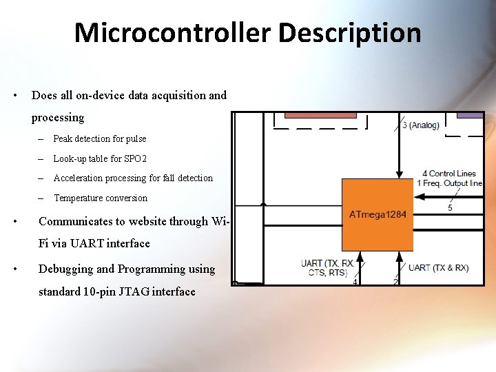
Microcontroller Description • Does all on-device data acquisition and processing – Peak detection for pulse – Look-up table for SPO 2 – Acceleration processing for fall detection – Temperature conversion • Communicates to website through Wi. Fi via UART interface • Debugging and Programming using standard 10 -pin JTAG interface
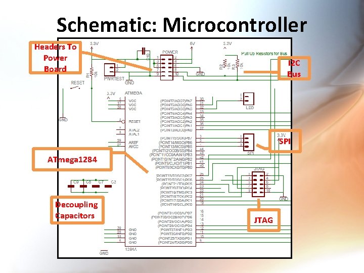
Schematic: Microcontroller Headers To Power Board I 2 C Bus SPI ATmega 1284 Decoupling Capacitors JTAG
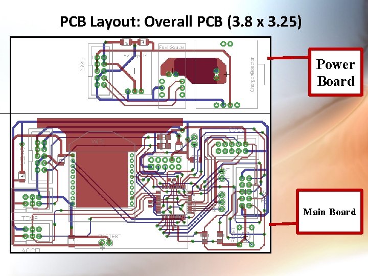
PCB Layout: Overall PCB (3. 8 x 3. 25) Power Board Main Board
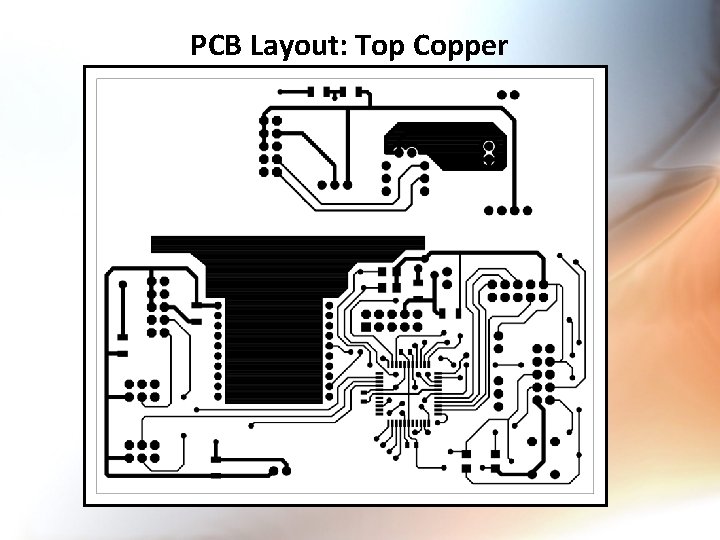
PCB Layout: Top Copper
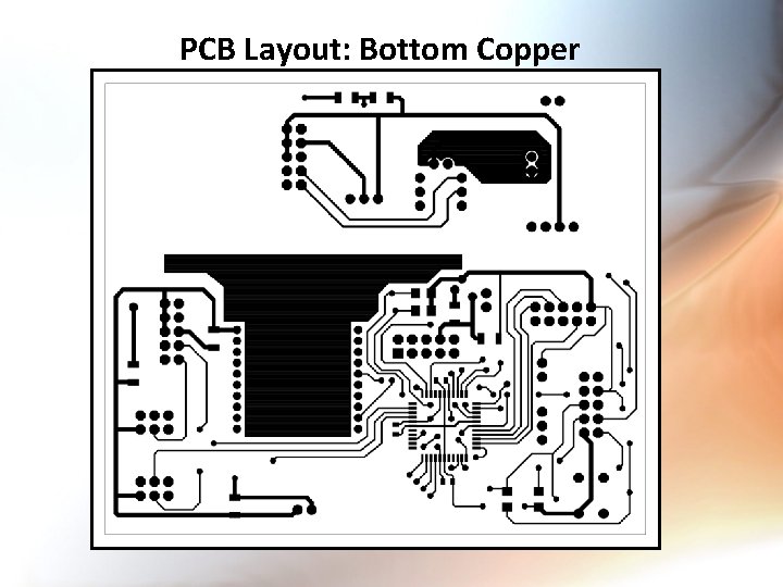
PCB Layout: Bottom Copper
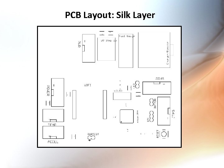
PCB Layout: Silk Layer
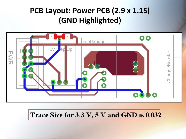
PCB Layout: Power PCB (2. 9 x 1. 15) (GND Highlighted) Trace Size for 3. 3 V, 5 V and GND is 0. 032
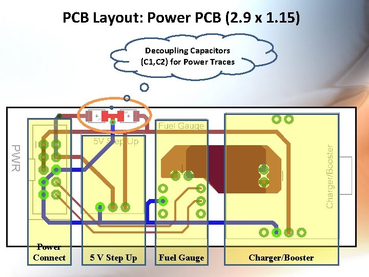
PCB Layout: Power PCB (2. 9 x 1. 15) Decoupling Capacitors (C 1, C 2) for Power Traces Power Connect 5 V Step Up Fuel Gauge Charger/Booster
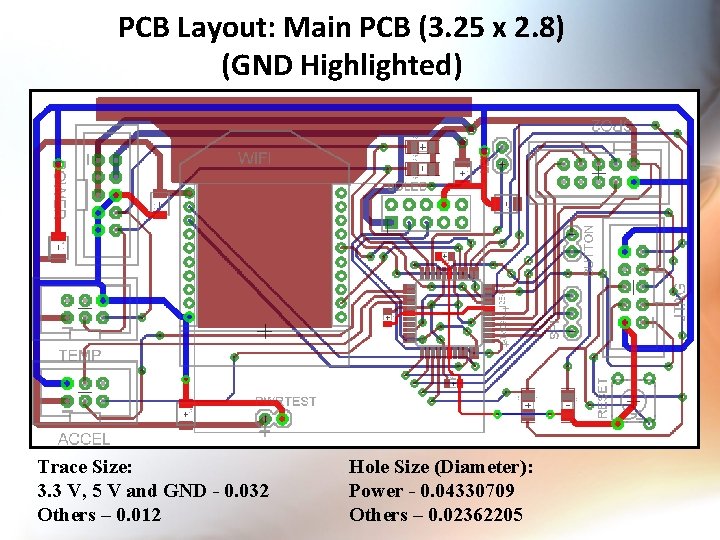
PCB Layout: Main PCB (3. 25 x 2. 8) (GND Highlighted) Trace Size: 3. 3 V, 5 V and GND - 0. 032 Others – 0. 012 Hole Size (Diameter): Power - 0. 04330709 Others – 0. 02362205
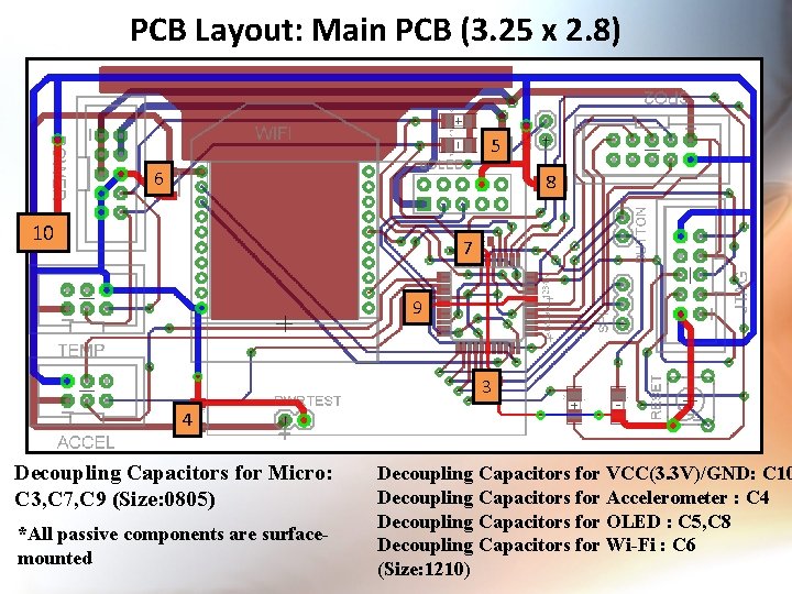
PCB Layout: Main PCB (3. 25 x 2. 8) 5 6 8 10 7 9 3 4 Decoupling Capacitors for Micro: C 3, C 7, C 9 (Size: 0805) *All passive components are surfacemounted Decoupling Capacitors for VCC(3. 3 V)/GND: C 10 Decoupling Capacitors for Accelerometer : C 4 Decoupling Capacitors for OLED : C 5, C 8 Decoupling Capacitors for Wi-Fi : C 6 (Size: 1210)
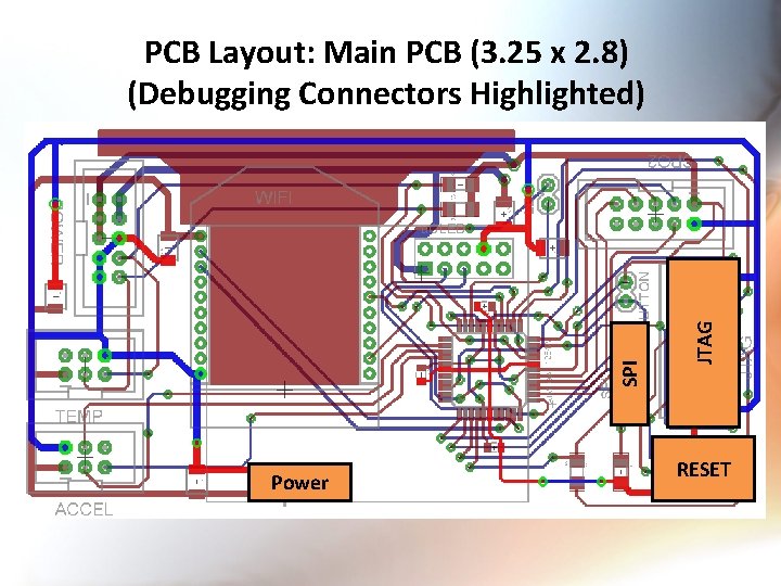
Power JTAG SPI PCB Layout: Main PCB (3. 25 x 2. 8) (Debugging Connectors Highlighted) RESET
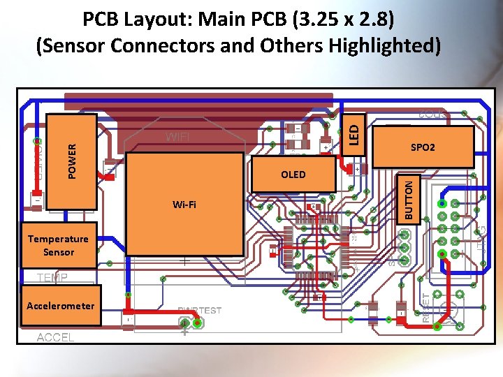
OLED Wi-Fi Temperature Sensor Accelerometer SPO 2 BUTTON POWER LED PCB Layout: Main PCB (3. 25 x 2. 8) (Sensor Connectors and Others Highlighted)
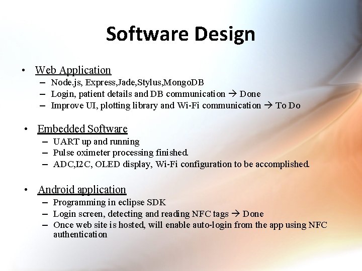
Software Design • Web Application – Node. js, Express, Jade, Stylus, Mongo. DB – Login, patient details and DB communication Done – Improve UI, plotting library and Wi-Fi communication To Do • Embedded Software – UART up and running – Pulse oximeter processing finished. – ADC, I 2 C, OLED display, Wi-Fi configuration to be accomplished. • Android application – Programming in eclipse SDK – Login screen, detecting and reading NFC tags Done – Once web site is hosted, will enable auto-login from the app using NFC authentication
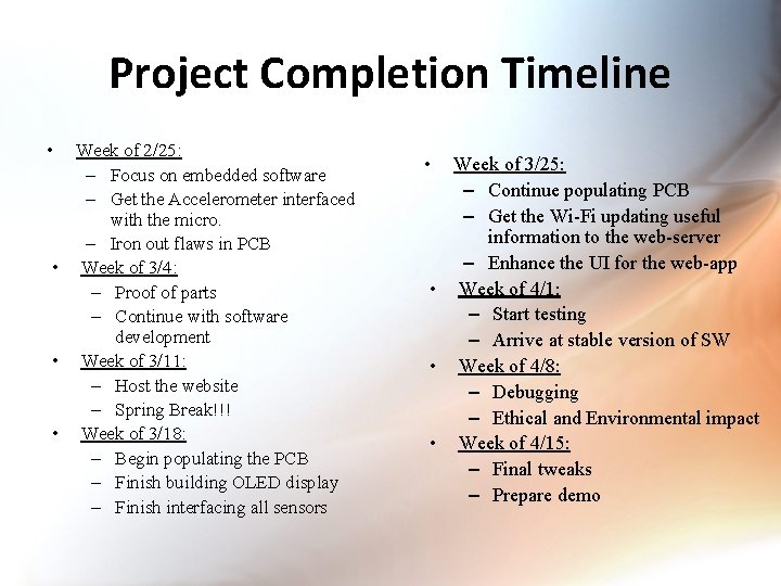
Project Completion Timeline • Week of 2/25: – Focus on embedded software – Get the Accelerometer interfaced with the micro. – Iron out flaws in PCB • Week of 3/4: – Proof of parts – Continue with software development • Week of 3/11: – Host the website – Spring Break!!! • Week of 3/18: – Begin populating the PCB – Finish building OLED display – Finish interfacing all sensors • Week of 3/25: – Continue populating PCB – Get the Wi-Fi updating useful information to the web-server – Enhance the UI for the web-app • Week of 4/1: – Start testing – Arrive at stable version of SW • Week of 4/8: – Debugging – Ethical and Environmental impact • Week of 4/15: – Final tweaks – Prepare demo

tio ns ? Qu es
- Slides: 39