Visible Light CMOS Image Sensors Dr Eric R
Visible Light CMOS Image Sensors Dr. Eric R. Fossum Senior Fellow, Micron Imaging Micron Technology, Inc.
Outline 4 Introduction to CMOS image sensor pixels 4 Examples of sensors 4 Customer trends 4 CMOS image sensor technology trend 4 Thoughts on next 5 years 6/17/2021 2
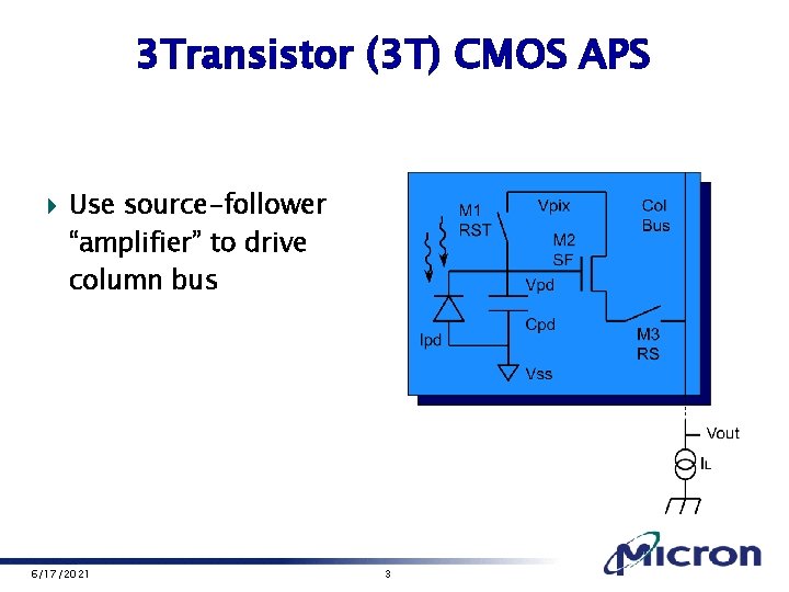
3 Transistor (3 T) CMOS APS 4 Use source-follower “amplifier” to drive column bus 6/17/2021 3
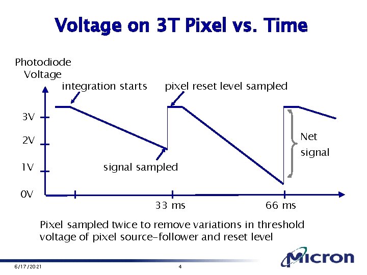
Voltage on 3 T Pixel vs. Time Photodiode Voltage integration starts pixel reset level sampled 3 V Net 2 V 1 V signal sampled 0 V 33 ms 66 ms Pixel sampled twice to remove variations in threshold voltage of pixel source-follower and reset level 6/17/2021 4

Simplified Signal Chain Photodiode Voltage integration starts PIXEL VDD pixel reset level sampled 3 V Net 2 V RST signal 1 V signal sampled 0 V 33 ms RS COL BUS SHS 66 ms GLOBAL CS SIG VLP HOR BUS SHR RST VLN PER COLUMN 6/17/2021 5 VLP
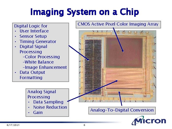
Imaging System on a Chip Digital Logic for • User Interface • Sensor Setup • Timing Generator • Digital Signal Processing –Color Processing –White Balance –Image Enhancement • Data Output Formatting CMOS Active Pixel Color Imaging Array Analog Signal Processing • Data Sampling • Noise Reduction • Gain 6/17/2021 Analog-To-Digital Conversion 6
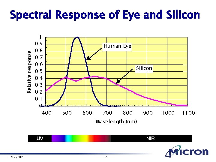
Relative response Spectral Response of Eye and Silicon 1 0. 9 0. 8 0. 7 0. 6 0. 5 0. 4 0. 3 0. 2 0. 1 0 400 Human Eye Silicon 500 600 700 800 900 Wavelength (nm) UV 6/17/2021 NIR 7 1000 1100
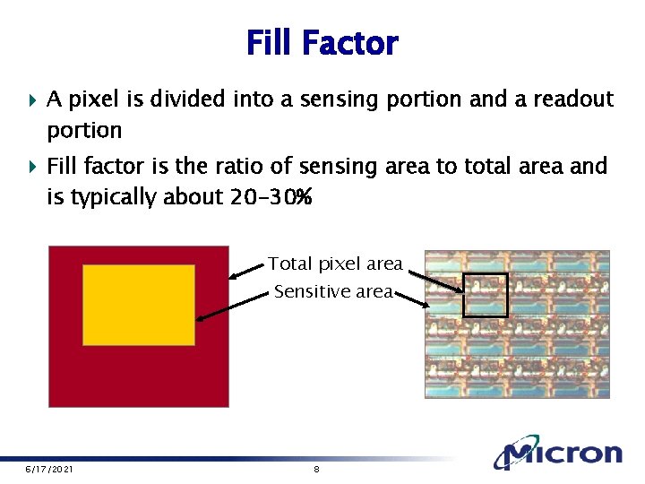
Fill Factor 4 A pixel is divided into a sensing portion and a readout portion 4 Fill factor is the ratio of sensing area to total area and is typically about 20 -30% Total pixel area Sensitive area 6/17/2021 8
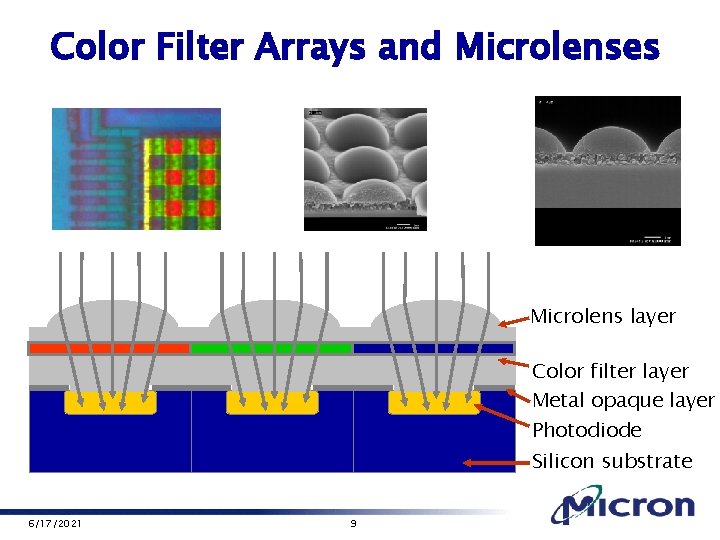
Color Filter Arrays and Microlenses Microlens layer Color filter layer Metal opaque layer Photodiode Silicon substrate 6/17/2021 9
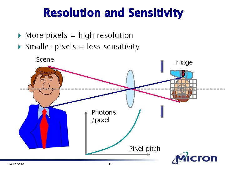
Resolution and Sensitivity 4 More pixels = high resolution 4 Smaller pixels = less sensitivity Scene Image Photons /pixel Pixel pitch 6/17/2021 10
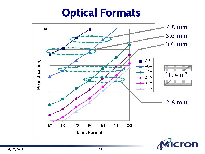
Optical Formats 7. 8 mm 5. 6 mm 3. 6 mm “ 1/4 in” 2. 8 mm 6/17/2021 11
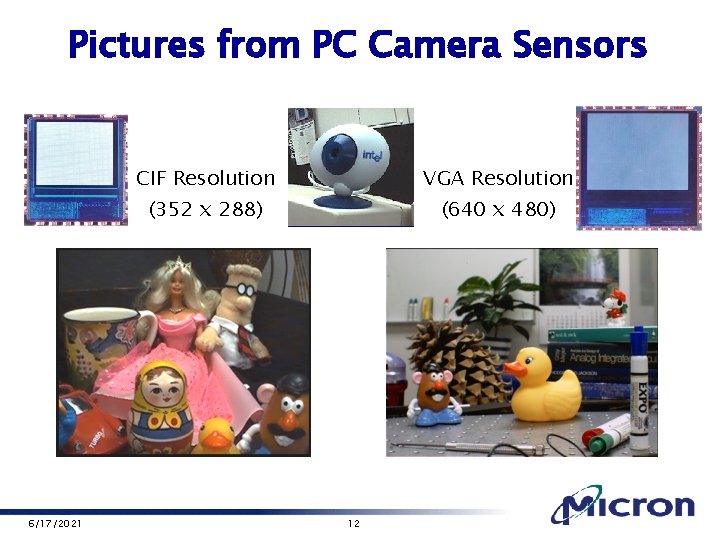
Pictures from PC Camera Sensors 6/17/2021 CIF Resolution VGA Resolution (352 x 288) (640 x 480) 12
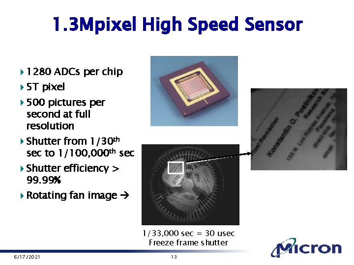
1. 3 Mpixel High Speed Sensor 41280 ADCs per chip 45 T pixel 4500 pictures per second at full resolution 4 Shutter from 1/30 th sec to 1/100, 000 th sec 4 Shutter efficiency > 99. 99% 4 Rotating fan image 1/33, 000 sec = 30 usec Freeze frame shutter 6/17/2021 13
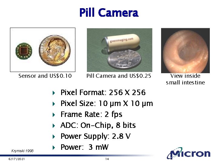
Pill Camera Sensor and US$0. 10 Pill Camera and US$0. 25 4 Pixel Format: 256 X 256 4 Pixel Size: 10 µm X 10 µm 4 Frame Rate: 2 fps 4 ADC: On-Chip, 8 bits 4 Power Supply: 2. 8 V Krymski 1998 6/17/2021 4 Power: 3 m. W 14 View inside small intestine
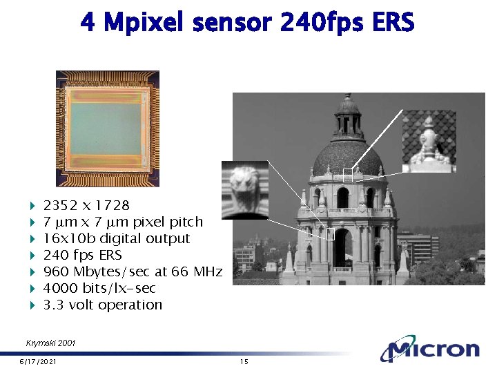
4 Mpixel sensor 240 fps ERS 4 4 4 4 2352 x 1728 7 m x 7 m pixel pitch 16 x 10 b digital output 240 fps ERS 960 Mbytes/sec at 66 MHz 4000 bits/lx-sec 3. 3 volt operation Krymski 2001 6/17/2021 15
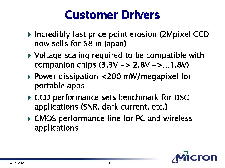
Customer Drivers 4 Incredibly fast price point erosion (2 Mpixel CCD now sells for $8 in Japan) 4 Voltage scaling required to be compatible with companion chips (3. 3 V -> 2. 8 V ->… 1. 8 V) 4 Power dissipation <200 m. W/megapixel for portable apps 4 CCD performance sets benchmark for DSC applications (SNR, dark current, etc. ) 4 CMOS performance fine for PC and wireless applications 6/17/2021 16
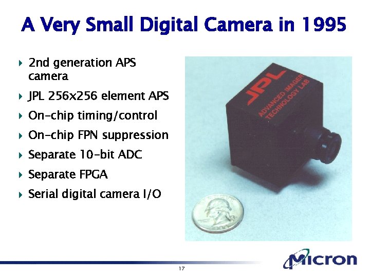
A Very Small Digital Camera in 1995 4 2 nd generation APS camera 4 JPL 256 x 256 element APS 4 On-chip timing/control 4 On-chip FPN suppression 4 Separate 10 -bit ADC 4 Separate FPGA 4 Serial digital camera I/O 17
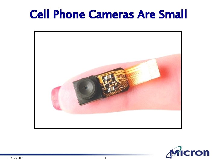
Cell Phone Cameras Are Small 6/17/2021 18
Technology Challenges 4 Smaller pixels 4 Maintain or improve SNR with smaller pixel 4 Maintain or increase dynamic range with lower operating voltages 4 Reduce dark current 4 Reduce number of defective pixels 4 Reduce power dissipation in analog and digital circuits while increasing functionality 6/17/2021 19
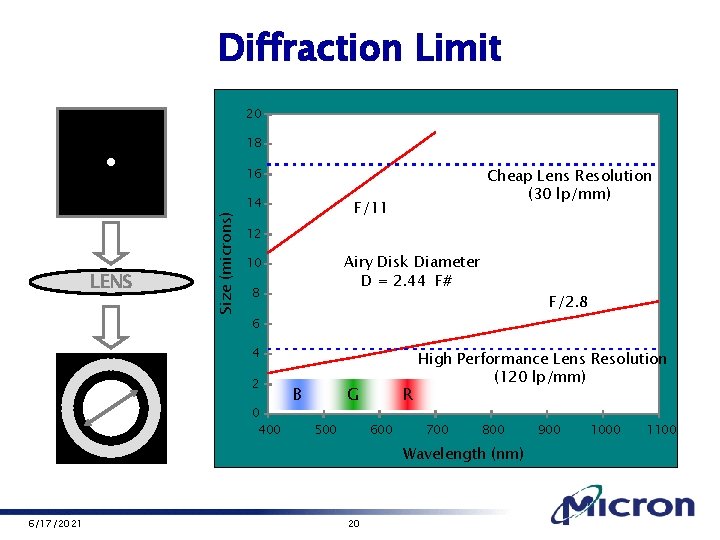
Diffraction Limit 20 18 LENS Size (microns) 16 14 Cheap Lens Resolution (30 lp/mm) F/11 12 Airy Disk Diameter D = 2. 44 F# 10 8 F/2. 8 6 4 2 0 400 BB G G 500 RR 600 High Performance Lens Resolution (120 lp/mm) 700 800 Wavelength (nm) 6/17/2021 20 900 1000 1100
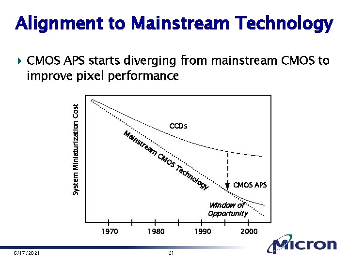
Alignment to Mainstream Technology 4 CMOS APS starts diverging from mainstream CMOS to System Miniaturization Cost improve pixel performance CCDs Ma in str ea m CM OS Te ch no lo gy CMOS APS Window of Opportunity 1970 6/17/2021 1980 1990 21 2000
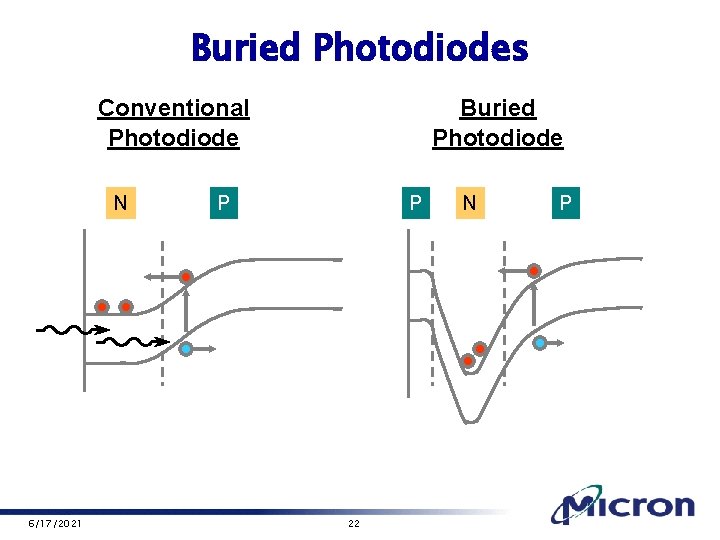
Buried Photodiodes Conventional Photodiode N 6/17/2021 Buried Photodiode P P 22 N P
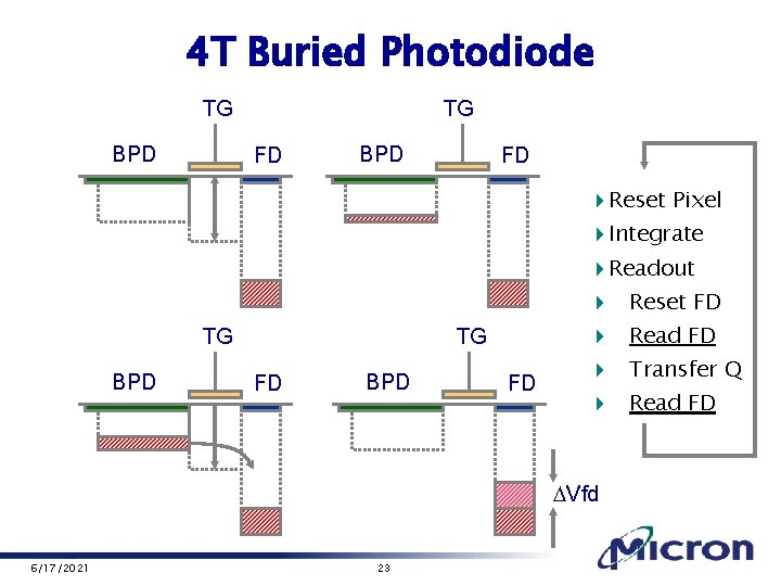
4 T Buried Photodiode TG BPD TG FD BPD FD 4 Reset Pixel 4 Integrate 4 Readout TG BPD TG FD BPD FD 4 Reset FD 4 Read FD 4 Transfer Q 4 Read FD DVfd 6/17/2021 23
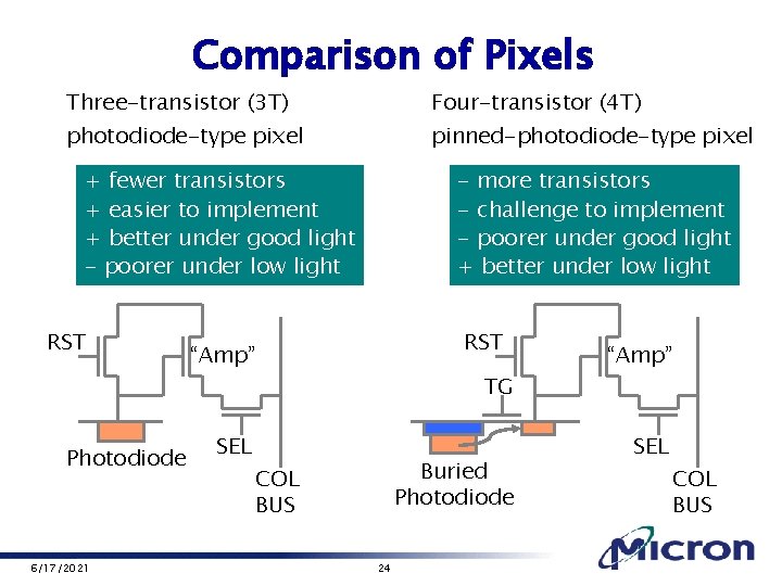
Comparison of Pixels Three-transistor (3 T) Four-transistor (4 T) photodiode-type pixel pinned-photodiode-type pixel + fewer transistors + easier to implement + better under good light - poorer under low light RST Photodiode 6/17/2021 - more transistors - challenge to implement - poorer under good light + better under low light RST “Amp” SEL TG Buried Photodiode COL BUS 24 “Amp” SEL COL BUS
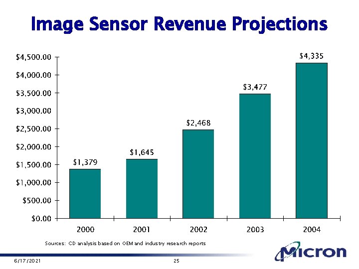
Image Sensor Revenue Projections Sources: CD analysis based on OEM and industry research reports 6/17/2021 25
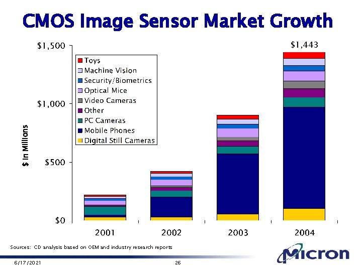
CMOS Image Sensor Market Growth $ in Millions $1, 443 Sources: CD analysis based on OEM and industry research reports 6/17/2021 26
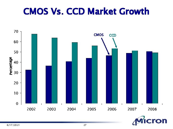
CMOS Vs. CCD Market Growth Percentage CMOS 6/17/2021 27 CCD
- Slides: 27