VIRTUAL MEMORY CACHE PHYSICAL MEMORY Why virtual memory








- Slides: 67

VIRTUAL MEMORY, CACHE, PHYSICAL MEMORY

Why virtual memory? • With a 32 -bit address you can access 4 GB of physical memory (you will never get the full memory though) – Seems enough for most day-to-day applications – But there are important applications that have much bigger memory footprint: databases, scientific apps operating on large matrices etc. – Even if your application fits entirely in physical memory it seems unfair to load the full image at startup – Just takes away memory from other processes, but probably doesn’t need the full image at any point of time during execution: hurts multiprogramming • Need to provide an illusion of bigger memory: Virtual Memory (VM) MAINAK CS 622 2

• Virtual memory Need an address to access virtual memory – Virtual Address (VA) • Assume a 32 -bit VA – Every process sees a 4 GB of virtual memory – This is much better than a 4 GB physical memory shared between multiprogrammed processes – The size of VA is really fixed by the processor data path width – 64 -bit processors (Alpha 21264, 21364; Sun Ultra. SPARC; AMD Athlon 64, Opteron; IBM POWER 4, POWER 5; MIPS R 10000 onwards; Intel Itanium etc. , and recently Intel Pentium 4, Intel Core 2 duo, etc. ) provide bigger virtual memory to each process – Large virtual and physical memory is very important in commercial server market: need to run large databases MAINAK CS 622 3

Addressing VM • There are primarily three ways to address VM – Paging, Segmentation, Segmented paging – We will focus on flat paging only • Paged VM – The entire VM is divided into small units called pages – Virtual pages are loaded into physical page frames as and when needed (demand paging) – Thus the physical memory is also divided into equal sized page frames – The processor generates virtual addresses – But memory is physically addressed: need a VA to PA translation MAINAK CS 622 4

VA to PA translation • The VA generated by the processor is divided into two parts: – Page offset and Virtual page number (VPN) – Assume a 4 KB page: within a 32 -bit VA, lower 12 bits will be page offset (offset within a page) and the remaining 20 bits are VPN (hence 1 M virtual pages total) – The page offset remains unchanged in the translation – Need to translate VPN to a physical page frame number (PPFN) – This translation is held in a page table resident in memory: so first we need to access this page table – How to get the address of the page table? MAINAK CS 622 5

VA to PA translation • Accessing the page table – The Page table base register (PTBR) contains the starting physical address of the page table – PTBR is normally accessible in the kernel mode only – Assume each entry in page table is 32 bits (4 bytes) – Thus the required page table address is PTBR + (VPN << 2) – Access memory at this address to get 32 bits of data from the page table entry (PTE) – These 32 bits contain many things: a valid bit, the much needed PPFN (may be 20 bits for a 4 GB physical memory), access permissions (read, write, execute), a dirty/modified bit etc. MAINAK CS 622 6

Page fault • The valid bit within the 32 bits tells you if the translation is valid • If this bit is reset that means the page is not resident in memory: results in a page fault • In case of a page fault the kernel needs to bring in the page to memory from disk • The disk address is normally provided by the page table entry (different interpretation of 31 bits) • Also kernel needs to allocate a new physical page frame for this virtual page • If all frames are occupied it invokes a page replacement policy MAINAK CS 622 7

VA to PA translation • Page faults take a long time: order of ms – Need a good page replacement policy • Once the page fault finishes, the page table entry is updated with the new VPN to PPFN mapping • Of course, if the valid bit was set, you get the PPFN right away without taking a page fault • Finally, PPFN is concatenated with the page offset to get the final PA PPFN Offset • Processor now can issue a memory request with this PA to get the necessary data • Really two memory accesses are needed • Can we improve on this? MAINAK CS 622 8

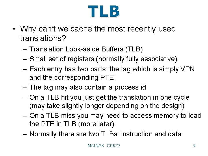
TLB • Why can’t we cache the most recently used translations? – Translation Look-aside Buffers (TLB) – Small set of registers (normally fully associative) – Each entry has two parts: the tag which is simply VPN and the corresponding PTE – The tag may also contain a process id – On a TLB hit you just get the translation in one cycle (may take slightly longer depending on the design) – On a TLB miss you may need to access memory to load the PTE in TLB (more later) – Normally there are two TLBs: instruction and data MAINAK CS 622 9

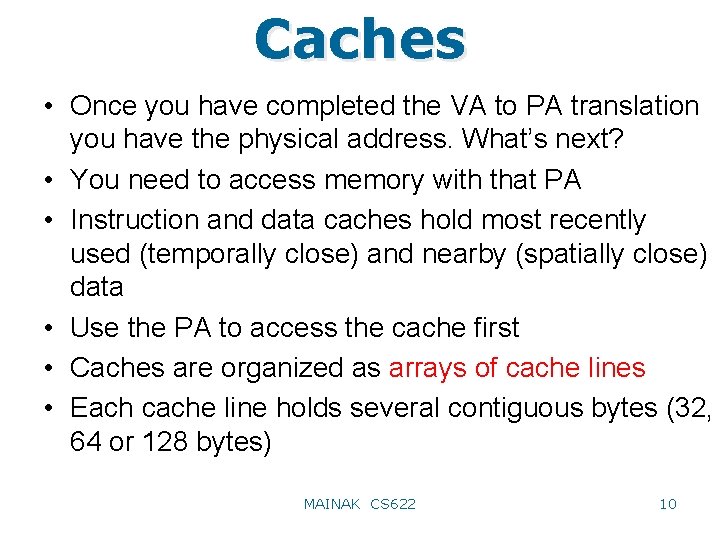
Caches • Once you have completed the VA to PA translation you have the physical address. What’s next? • You need to access memory with that PA • Instruction and data caches hold most recently used (temporally close) and nearby (spatially close) data • Use the PA to access the cache first • Caches are organized as arrays of cache lines • Each cache line holds several contiguous bytes (32, 64 or 128 bytes) MAINAK CS 622 10

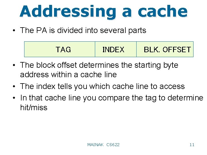
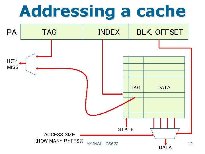
Addressing a cache • The PA is divided into several parts TAG INDEX BLK. OFFSET • The block offset determines the starting byte address within a cache line • The index tells you which cache line to access • In that cache line you compare the tag to determine hit/miss MAINAK CS 622 11

Addressing a cache PA TAG INDEX BLK. OFFSET HIT/ MISS TAG DATA STATE ACCESS SIZE (HOW MANY BYTES? ) MAINAK CS 622 DATA 12

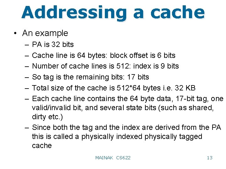
Addressing a cache • An example – – – PA is 32 bits Cache line is 64 bytes: block offset is 6 bits Number of cache lines is 512: index is 9 bits So tag is the remaining bits: 17 bits Total size of the cache is 512*64 bytes i. e. 32 KB Each cache line contains the 64 byte data, 17 -bit tag, one valid/invalid bit, and several state bits (such as shared, dirty etc. ) – Since both the tag and the index are derived from the PA this is called a physically indexed physically tagged cache MAINAK CS 622 13

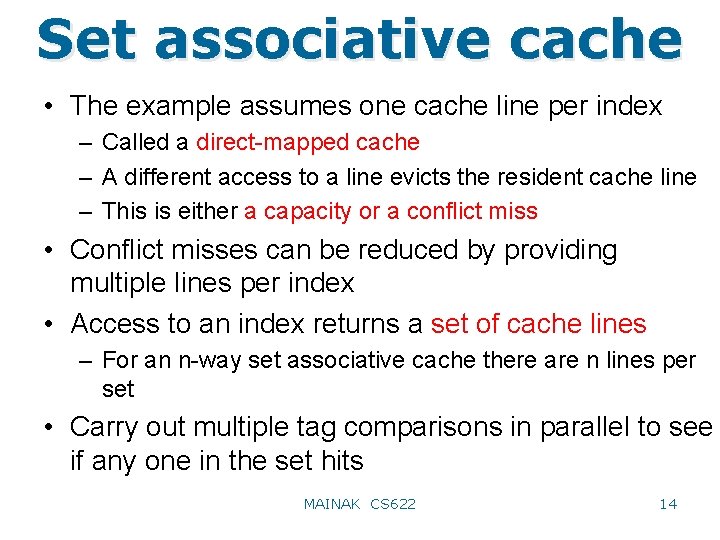
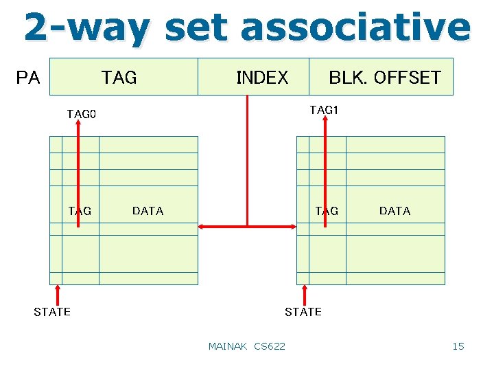
Set associative cache • The example assumes one cache line per index – Called a direct-mapped cache – A different access to a line evicts the resident cache line – This is either a capacity or a conflict miss • Conflict misses can be reduced by providing multiple lines per index • Access to an index returns a set of cache lines – For an n-way set associative cache there are n lines per set • Carry out multiple tag comparisons in parallel to see if any one in the set hits MAINAK CS 622 14

2 -way set associative TAG PA INDEX TAG 1 TAG 0 TAG STATE BLK. OFFSET DATA TAG DATA STATE MAINAK CS 622 15

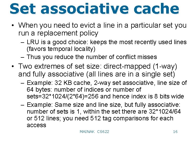
Set associative cache • When you need to evict a line in a particular set you run a replacement policy – LRU is a good choice: keeps the most recently used lines (favors temporal locality) – Thus you reduce the number of conflict misses • Two extremes of set size: direct-mapped (1 -way) and fully associative (all lines are in a single set) – Example: 32 KB cache, 2 -way set associative, line size of 64 bytes: number of indices or number of sets=32*1024/(2*64)=256 and hence index is 8 bits wide – Example: Same size and line size, but fully associative: number of sets is 1, within the set there are 32*1024/64 or 512 lines; you need 512 tag comparisons for each access MAINAK CS 622 16

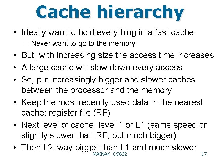
Cache hierarchy • Ideally want to hold everything in a fast cache – Never want to go to the memory • But, with increasing size the access time increases • A large cache will slow down every access • So, put increasingly bigger and slower caches between the processor and the memory • Keep the most recently used data in the nearest cache: register file (RF) • Next level of cache: level 1 or L 1 (same speed or slightly slower than RF, but much bigger) • Then L 2: way bigger than L 1 and much slower MAINAK CS 622 17

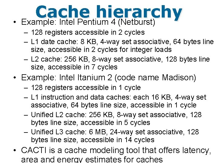
• Cache hierarchy Example: Intel Pentium 4 (Netburst) – 128 registers accessible in 2 cycles – L 1 date cache: 8 KB, 4 -way set associative, 64 bytes line size, accessible in 2 cycles for integer loads – L 2 cache: 256 KB, 8 -way set associative, 128 bytes line size, accessible in 7 cycles • Example: Intel Itanium 2 (code name Madison) – 128 registers accessible in 1 cycle – L 1 instruction and data caches: each 16 KB, 4 -way set associative, 64 bytes line size, accessible in 1 cycle – Unified L 2 cache: 256 KB, 8 -way set associative, 128 bytes line size, accessible in 5 cycles – Unified L 3 cache: 6 MB, 24 -way set associative, 128 bytes line size, accessible in 14 cycles • CACTI is a cache modeling tool that offers latency, area and energy estimates for caches

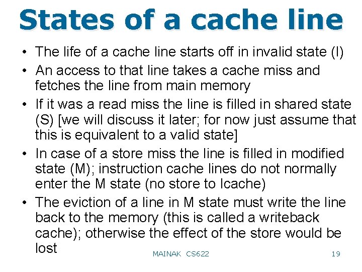
States of a cache line • The life of a cache line starts off in invalid state (I) • An access to that line takes a cache miss and fetches the line from main memory • If it was a read miss the line is filled in shared state (S) [we will discuss it later; for now just assume that this is equivalent to a valid state] • In case of a store miss the line is filled in modified state (M); instruction cache lines do not normally enter the M state (no store to Icache) • The eviction of a line in M state must write the line back to the memory (this is called a writeback cache); otherwise the effect of the store would be lost 19 MAINAK CS 622

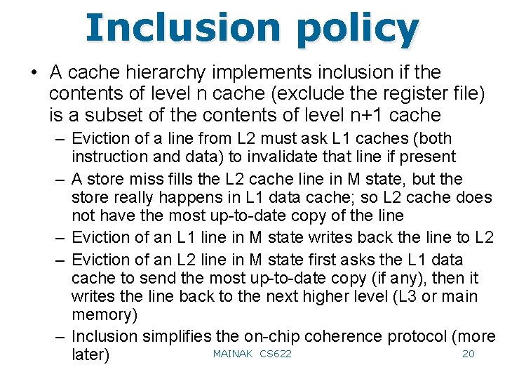
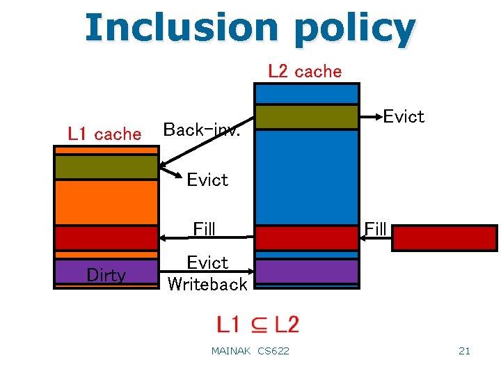
Inclusion policy • A cache hierarchy implements inclusion if the contents of level n cache (exclude the register file) is a subset of the contents of level n+1 cache – Eviction of a line from L 2 must ask L 1 caches (both instruction and data) to invalidate that line if present – A store miss fills the L 2 cache line in M state, but the store really happens in L 1 data cache; so L 2 cache does not have the most up-to-date copy of the line – Eviction of an L 1 line in M state writes back the line to L 2 – Eviction of an L 2 line in M state first asks the L 1 data cache to send the most up-to-date copy (if any), then it writes the line back to the next higher level (L 3 or main memory) – Inclusion simplifies the on-chip coherence protocol (more 20 MAINAK CS 622 later)

Inclusion policy L 2 cache L 1 cache Back-inv. Evict Fill Dirty Fill Evict Writeback MAINAK CS 622 21

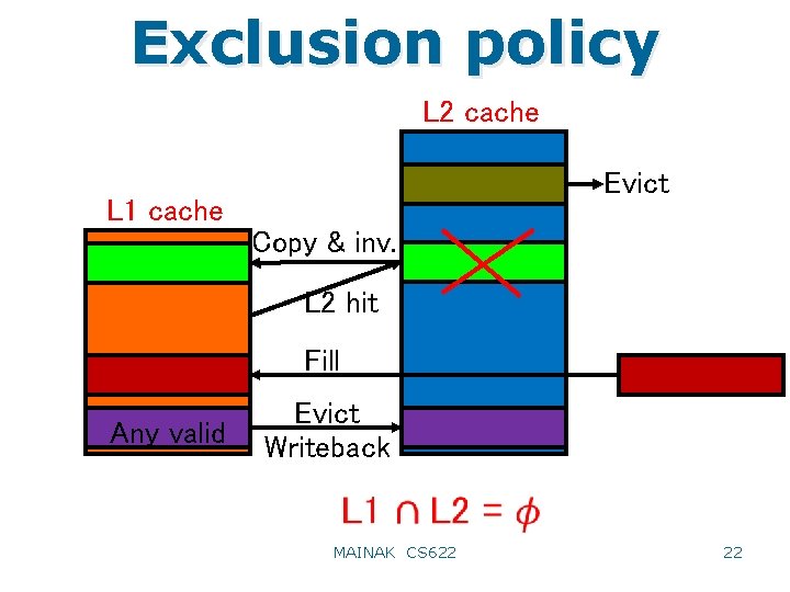
Exclusion policy L 2 cache Evict L 1 cache Copy & inv. L 2 hit Fill Any valid Evict Writeback MAINAK CS 622 22

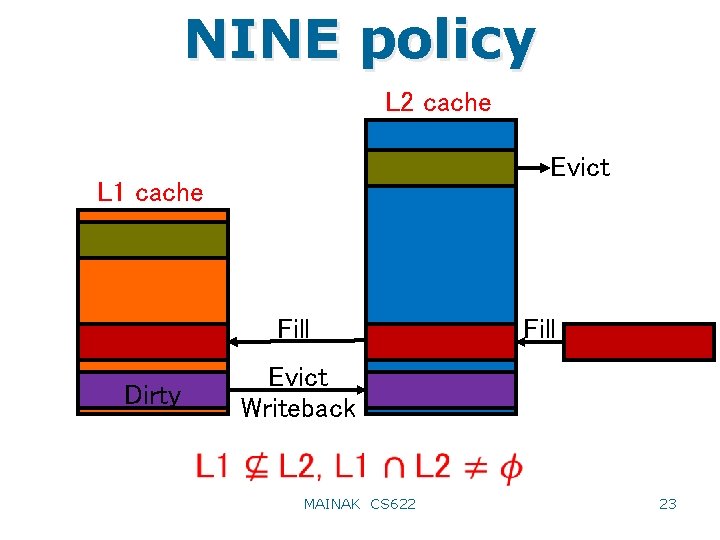
NINE policy L 2 cache Evict L 1 cache Fill Dirty Fill Evict Writeback MAINAK CS 622 23

The first instruction • Accessing the first instruction – – – Take the starting PC Access i. TLB with the VPN extracted from PC: i. TLB miss Invoke i. TLB miss handler Calculate PTE address If PTEs are cached in L 1 data and L 2 caches, look them up with PTE address: you will miss there also – Access page table in main memory: PTE is invalid: page fault – Invoke page fault handler – Allocate page frame, read page from disk, update PTE, load PTE in i. TLB, restart fetch MAINAK CS 622 24

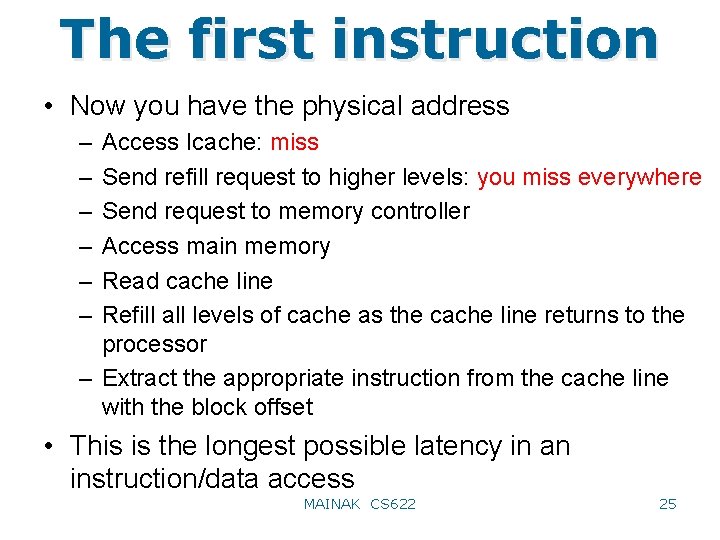
The first instruction • Now you have the physical address – – – Access Icache: miss Send refill request to higher levels: you miss everywhere Send request to memory controller Access main memory Read cache line Refill all levels of cache as the cache line returns to the processor – Extract the appropriate instruction from the cache line with the block offset • This is the longest possible latency in an instruction/data access MAINAK CS 622 25

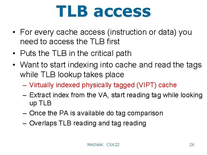
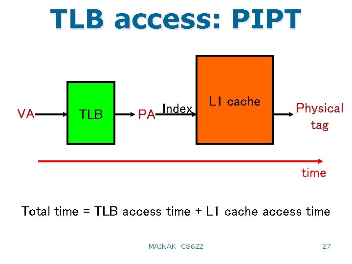
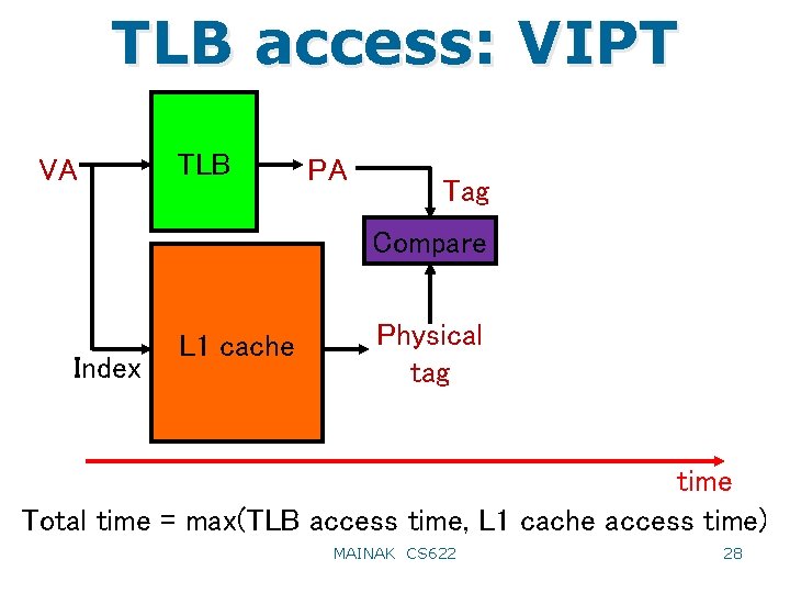
TLB access • For every cache access (instruction or data) you need to access the TLB first • Puts the TLB in the critical path • Want to start indexing into cache and read the tags while TLB lookup takes place – Virtually indexed physically tagged (VIPT) cache – Extract index from the VA, start reading tag while looking up TLB – Once the PA is available do tag comparison – Overlaps TLB reading and tag reading MAINAK CS 622 26

TLB access: PIPT VA TLB PA Index L 1 cache Physical tag time Total time = TLB access time + L 1 cache access time MAINAK CS 622 27

TLB access: VIPT VA TLB PA Tag Compare Index L 1 cache Physical tag time Total time = max(TLB access time, L 1 cache access time) MAINAK CS 622 28

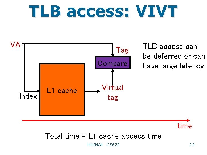
TLB access: VIVT VA Tag Compare Index L 1 cache TLB access can be deferred or can have large latency Virtual tag time Total time = L 1 cache access time MAINAK CS 622 29

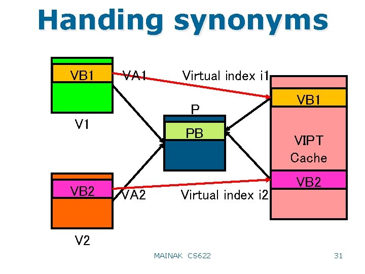
Handing synonyms • A correctness problem arises in VIVT and VIPT caches – Consider two virtual pages V 1 and V 2 that map to the same physical page P • Such mapping is often used to share data/code between different processes • V 1 and V 2 are called synonyms because they refer to the same physical data • Now consider a particular cache block VB 1 in V 1 which gets modified through some access; suppose this block resides at virtual index i 1 in the cache • Later another access touches the corresponding block VB 2 in V 2 through a different virtual index i 2 and gets 30 MAINAK CS 622 stale data

Handing synonyms VB 1 VA 1 Virtual index i 1 P V 1 VB 2 PB VA 2 Virtual index i 2 VB 1 VIPT Cache VB 2 V 2 MAINAK CS 622 31

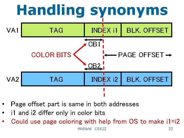
Handling synonyms VA 1 TAG INDEX i 1 BLK. OFFSET CB 1 COLOR BITS PAGE OFFSET CB 2 VA 2 TAG INDEX i 2 BLK. OFFSET • Page offset part is same in both addresses • i 1 and i 2 differ only in color bits • Could use page coloring with help from OS to make i 1=i 2 MAINAK CS 622 32

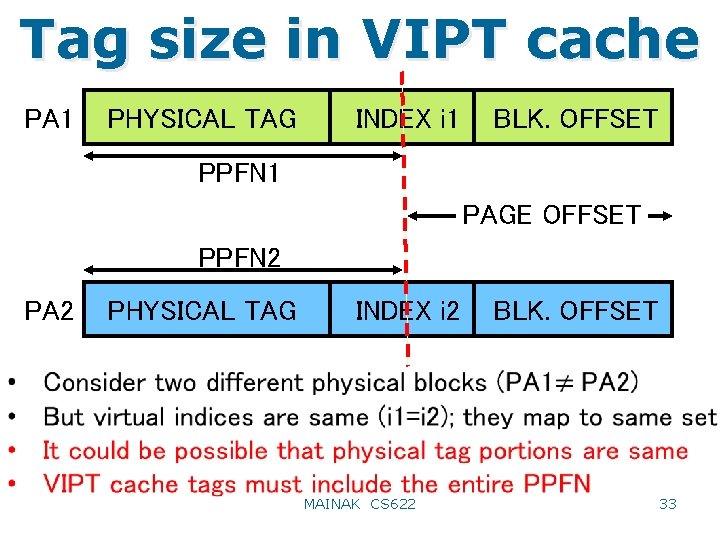
Tag size in VIPT cache PA 1 PHYSICAL TAG INDEX i 1 BLK. OFFSET PPFN 1 PAGE OFFSET PPFN 2 PA 2 PHYSICAL TAG INDEX i 2 MAINAK CS 622 BLK. OFFSET 33

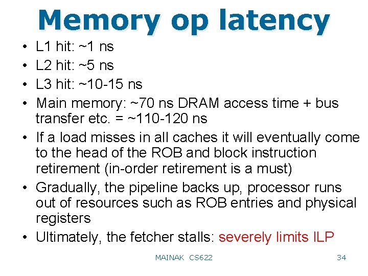
Memory op latency • • L 1 hit: ~1 ns L 2 hit: ~5 ns L 3 hit: ~10 -15 ns Main memory: ~70 ns DRAM access time + bus transfer etc. = ~110 -120 ns • If a load misses in all caches it will eventually come to the head of the ROB and block instruction retirement (in-order retirement is a must) • Gradually, the pipeline backs up, processor runs out of resources such as ROB entries and physical registers • Ultimately, the fetcher stalls: severely limits ILP MAINAK CS 622 34

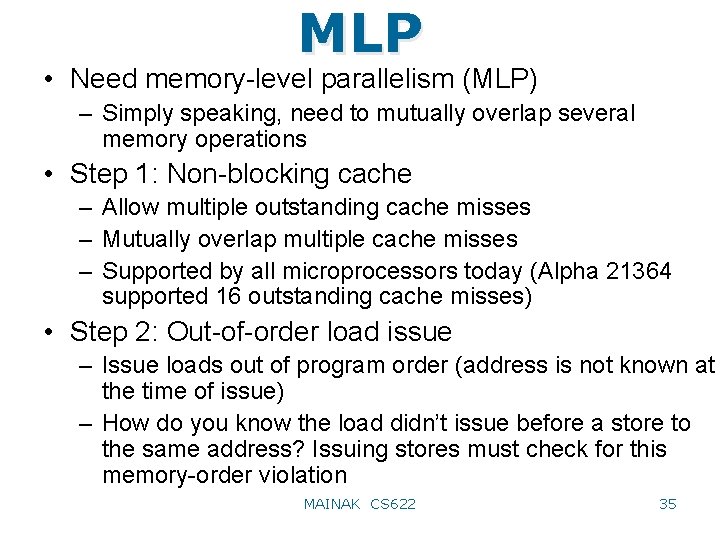
MLP • Need memory-level parallelism (MLP) – Simply speaking, need to mutually overlap several memory operations • Step 1: Non-blocking cache – Allow multiple outstanding cache misses – Mutually overlap multiple cache misses – Supported by all microprocessors today (Alpha 21364 supported 16 outstanding cache misses) • Step 2: Out-of-order load issue – Issue loads out of program order (address is not known at the time of issue) – How do you know the load didn’t issue before a store to the same address? Issuing stores must check for this memory-order violation MAINAK CS 622 35

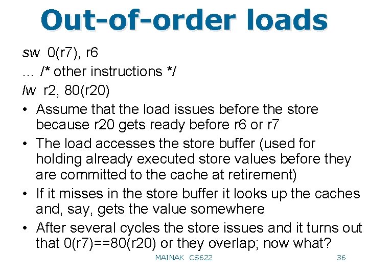
Out-of-order loads sw 0(r 7), r 6 … /* other instructions */ lw r 2, 80(r 20) • Assume that the load issues before the store because r 20 gets ready before r 6 or r 7 • The load accesses the store buffer (used for holding already executed store values before they are committed to the cache at retirement) • If it misses in the store buffer it looks up the caches and, say, gets the value somewhere • After several cycles the store issues and it turns out that 0(r 7)==80(r 20) or they overlap; now what? MAINAK CS 622 36

Load/store ordering • Out-of-order load issue relies on speculative memory disambiguation – Assumes that there will be no conflicting store – If the speculation is correct, you have issued the load much earlier and you have allowed the dependents to also execute much earlier – If there is a conflicting store, you have to squash the load and all the dependents that have consumed the load value and re-execute them systematically – Turns out that the speculation is correct most of the time – To further minimize the load squash, microprocessors use simple memory dependence predictors (predicts if a load is going to conflict with a pending store based on that load’s or load/store pairs’ past behavior) MAINAK CS 622 37

MLP and memory wall • Today microprocessors try to hide cache misses by initiating early prefetches: – Hardware prefetchers try to predict next several load addresses and initiate cache line prefetch if they are not already in the cache – All processors today also support prefetch instructions; so you can specify in your program when to prefetch what: this gives much better control compared to a hardware prefetcher • Researchers have worked on load value prediction • Even after doing all these, memory latency remains the biggest bottleneck • Today microprocessors are trying to overcome one single wall: the memory wall MAINAK CS 622 38

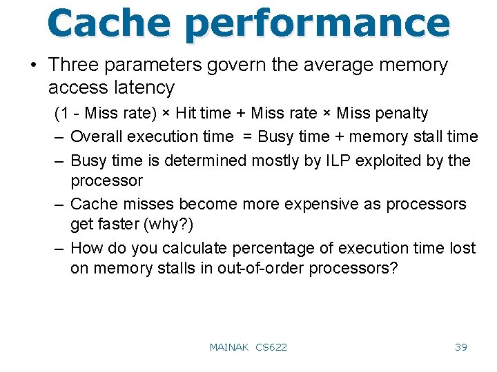
Cache performance • Three parameters govern the average memory access latency (1 - Miss rate) × Hit time + Miss rate × Miss penalty – Overall execution time = Busy time + memory stall time – Busy time is determined mostly by ILP exploited by the processor – Cache misses become more expensive as processors get faster (why? ) – How do you calculate percentage of execution time lost on memory stalls in out-of-order processors? MAINAK CS 622 39

Miss penalty • Which instruction is more affected: load or store? • How to reduce miss penalty? – Multi-level caches: equation for memory access latency? • Local miss rate and global miss rate • Misses per instruction • Inclusion/exclusion? • Large or fast L 2? Block size and associativity? Comparison with L 1? – Critical word first: fetch the missed word first – Early restart: fetch in order, but start as soon as possible • Problems? (next access) – Prioritize loads: • Put stores in write buffers for write-through cache? • Fill before spill in writeback cache MAINAK CS 622 40

Miss penalty • How to reduce miss penalty? – Victim cache • A small fully associative buffer containing last few evicted cache lines • Victim cache hit swaps replaced cache line with it • Increases effective associativity of the cache • AMD Athlon has 8 victim buffers MAINAK CS 622 41

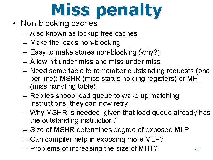
Miss penalty • Non-blocking caches – – – – – Also known as lockup-free caches Make the loads non-blocking Easy to make stores non-blocking (why? ) Allow hit under miss and miss under miss Need some table to remember outstanding requests (one per line): MSHR (miss status holding registers) or MHT (miss handling table) Replies snoop load queue to wake up matching instructions; they can now retry Why MSHR is needed, given that load queue already has the outstanding instruction? Size of MSHR determines degree of exposed MLP Can compiler help in exposing more MLP? 42 Problems of increasing the size of MHT?

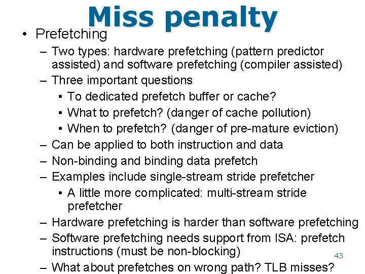
• Miss penalty Prefetching – Two types: hardware prefetching (pattern predictor assisted) and software prefetching (compiler assisted) – Three important questions • To dedicated prefetch buffer or cache? • What to prefetch? (danger of cache pollution) • When to prefetch? (danger of pre-mature eviction) – Can be applied to both instruction and data – Non-binding and binding data prefetch – Examples include single-stream stride prefetcher • A little more complicated: multi-stream stride prefetcher – Hardware prefetching is harder than software prefetching – Software prefetching needs support from ISA: prefetch instructions (must be non-blocking) 43 – What about prefetches on wrong path? TLB misses?

Miss penalty • Cold store misses – Initialization often writes to entire cache line – Write hint instruction in Alpha 21264 – Needs compiler assistance MAINAK CS 622 44

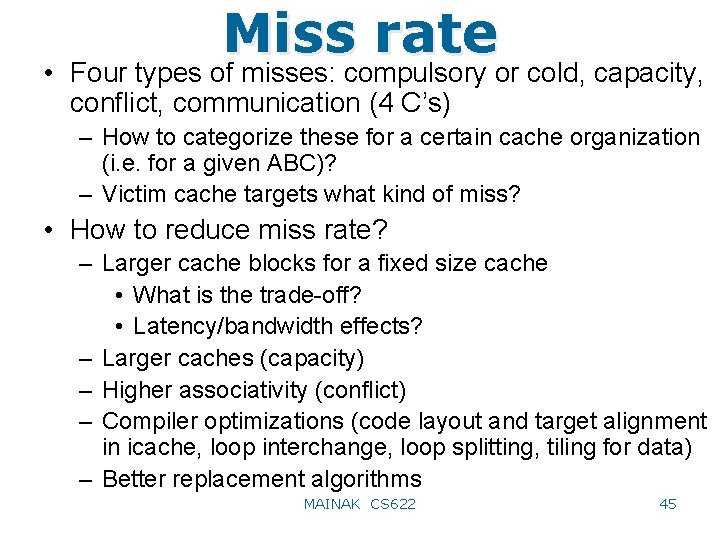
Miss rate • Four types of misses: compulsory or cold, capacity, conflict, communication (4 C’s) – How to categorize these for a certain cache organization (i. e. for a given ABC)? – Victim cache targets what kind of miss? • How to reduce miss rate? – Larger cache blocks for a fixed size cache • What is the trade-off? • Latency/bandwidth effects? – Larger caches (capacity) – Higher associativity (conflict) – Compiler optimizations (code layout and target alignment in icache, loop interchange, loop splitting, tiling for data) – Better replacement algorithms MAINAK CS 622 45

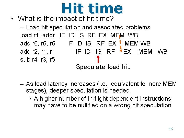
Hit time • What is the impact of hit time? – Load hit speculation and associated problems load r 1, addr IF ID IS RF EX MEM WB add r 6, r 6 IF ID IS RF EX MEM WB add r 2, r 1 IF ID IS RF EX MEM WB sub r 4, r 3, r 5 Speculate load hit – As load latency increases (i. e. , equivalent to more MEM stages), deeper speculation is needed • A higher number of in-flight dependent instructions may have to be nullified on a wrong hit speculation 46

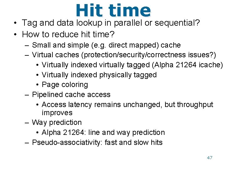
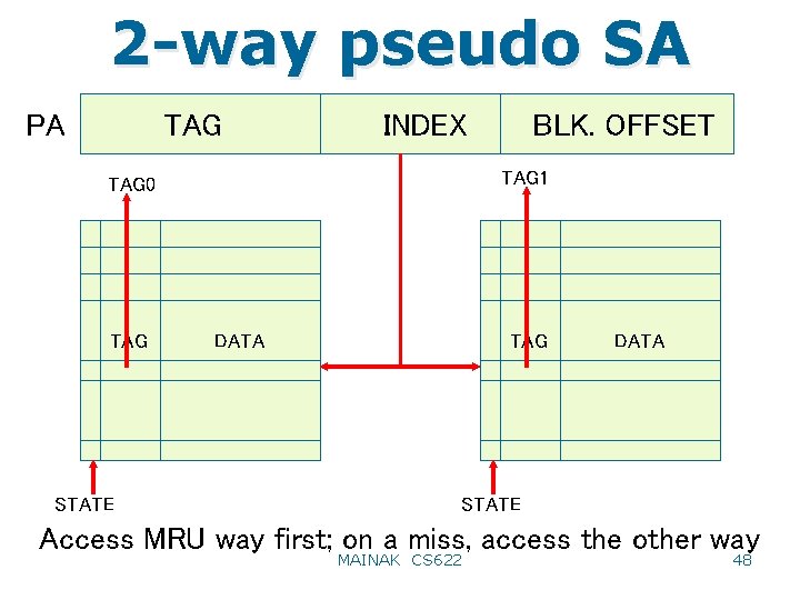
Hit time • Tag and data lookup in parallel or sequential? • How to reduce hit time? – Small and simple (e. g. direct mapped) cache – Virtual caches (protection/security/correctness issues? ) • Virtually indexed virtually tagged (Alpha 21264 icache) • Virtually indexed physically tagged • Page coloring – Pipelined cache access • Access latency remains unchanged, but throughput improves – Way prediction • Alpha 21264: line and way prediction – Pseudo-associativity: fast and slow hits 47

2 -way pseudo SA TAG PA INDEX TAG 1 TAG 0 TAG STATE BLK. OFFSET DATA TAG DATA STATE Access MRU way first; on a miss, access the other way MAINAK CS 622 48

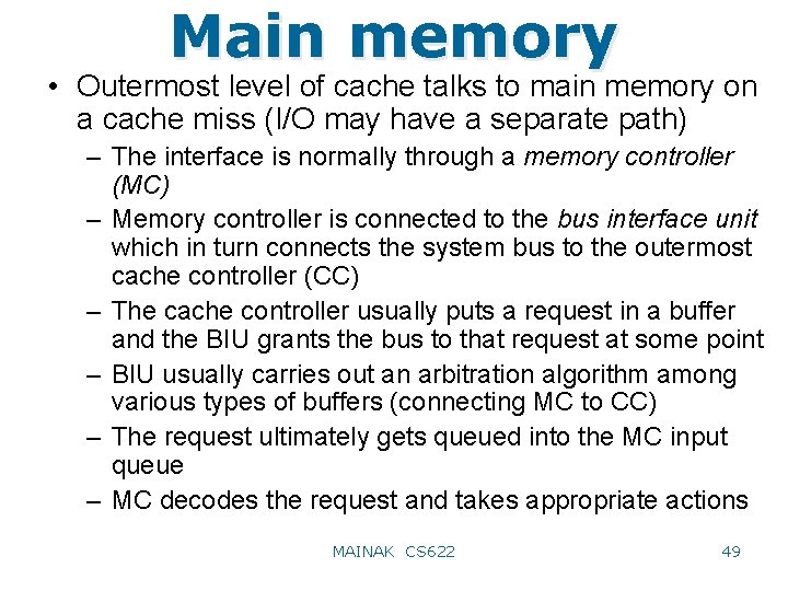
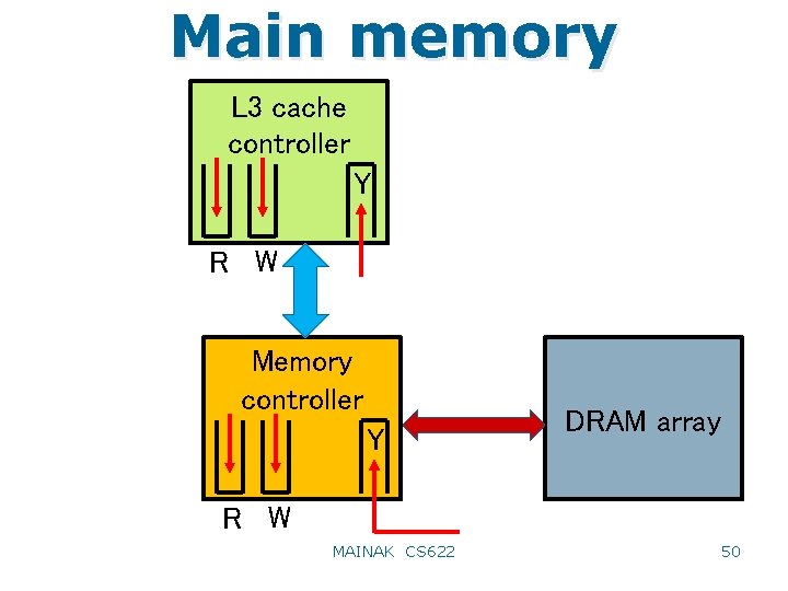
Main memory • Outermost level of cache talks to main memory on a cache miss (I/O may have a separate path) – The interface is normally through a memory controller (MC) – Memory controller is connected to the bus interface unit which in turn connects the system bus to the outermost cache controller (CC) – The cache controller usually puts a request in a buffer and the BIU grants the bus to that request at some point – BIU usually carries out an arbitration algorithm among various types of buffers (connecting MC to CC) – The request ultimately gets queued into the MC input queue – MC decodes the request and takes appropriate actions MAINAK CS 622 49

Main memory L 3 cache controller Y R W Memory controller Y DRAM array R W MAINAK CS 622 50

Main memory • Steps involved in serving a cache miss from the outermost level (beyond miss detection) – Queue miss request in BIU buffer • How many request types (and hence how many different logical queues)? – BIU schedules the request and switches address, control, data (if needed) according to bus protocol – Request is fielded at the other end by MC and is put in a queue – MC picks requests out of this queue (normally in-order), decodes request type and address, and sends it to DRAM (dynamic random access memory) – DRAM access involves decoding row, decoding column, and reading out data (lumped together as access time) – Data reply is fielded by MC (DRAM bus connecting MC) 51 and put in a BIU queue for scheduling

Main memory • Latency and bandwidth – – – Understanding the trade-off Compute-bound and memory-bound applications Latency-bound applications Bandwidth-bound applications Easy to improve bandwidth: wide memory and bus, interleaving, banking, smart scheduling, … – Bank conflict and bank controllers – How to improve latency? • Architectural techniques: mostly revolves around “hiding” techniques • Lower-level techniques: deals with DRAM technology MAINAK CS 622 52

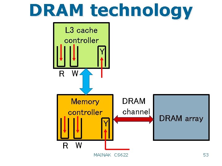
DRAM technology L 3 cache controller Y R W DRAM channel Memory controller Y DRAM array R W MAINAK CS 622 53

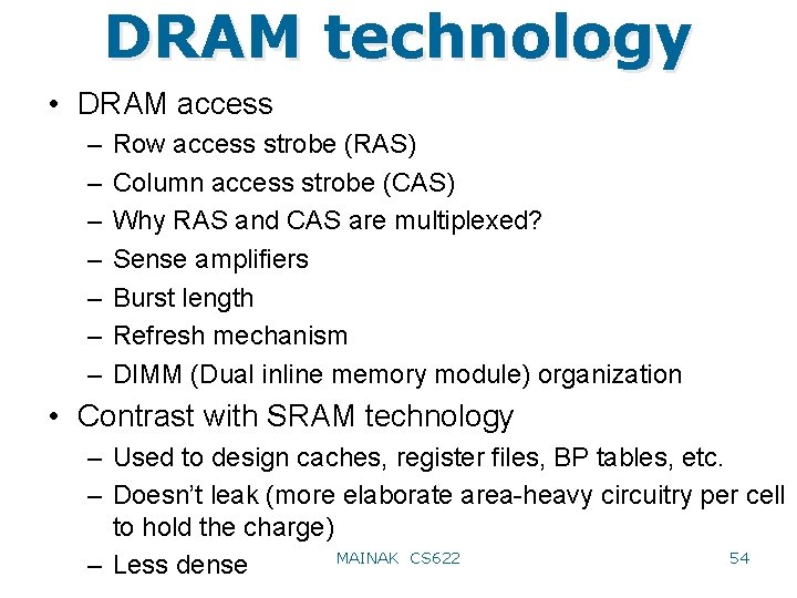
DRAM technology • DRAM access – – – – Row access strobe (RAS) Column access strobe (CAS) Why RAS and CAS are multiplexed? Sense amplifiers Burst length Refresh mechanism DIMM (Dual inline memory module) organization • Contrast with SRAM technology – Used to design caches, register files, BP tables, etc. – Doesn’t leak (more elaborate area-heavy circuitry per cell to hold the charge) 54 MAINAK CS 622 – Less dense

• Research problems Last-level caches (LLCs) are important for performance – Gap between state-of-the-art and Belady’s MIN is large – Can view the LLC as a seven-tuple <A, B, C, R, F, I, T> – For fixed ABCT, how do you optimize R, F, and I • R is really a composition of three components: insertion age, age update, victim selection • Good F can improve hit rate and hit latency in NUCAs • Inclusion vs exclusion is a bandwidth-capacity tradeoff; clever schemes can reduce bandwidth while offering good performance – All these optimizations must be done while keeping the energy consumption in mind; often energy-delay or energy-delay^2 is used as a metric 55 MAINAK CS 622

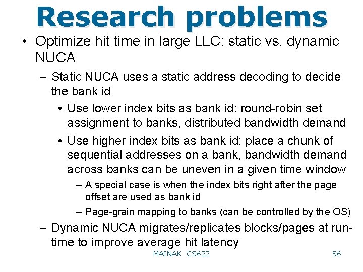
Research problems • Optimize hit time in large LLC: static vs. dynamic NUCA – Static NUCA uses a static address decoding to decide the bank id • Use lower index bits as bank id: round-robin set assignment to banks, distributed bandwidth demand • Use higher index bits as bank id: place a chunk of sequential addresses on a bank, bandwidth demand across banks can be uneven in a given time window – A special case is when the index bits right after the page offset are used as bank id – Page-grain mapping to banks (can be controlled by the OS) – Dynamic NUCA migrates/replicates blocks/pages at runtime to improve average hit latency MAINAK CS 622 56

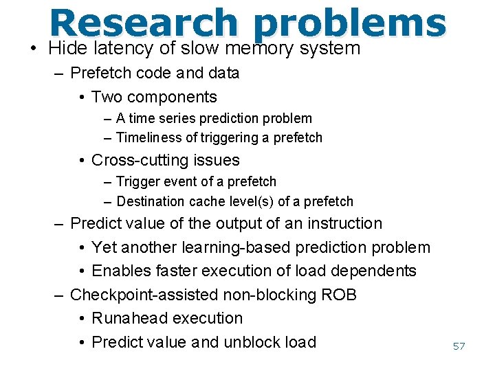
• Research problems Hide latency of slow memory system – Prefetch code and data • Two components – A time series prediction problem – Timeliness of triggering a prefetch • Cross-cutting issues – Trigger event of a prefetch – Destination cache level(s) of a prefetch – Predict value of the output of an instruction • Yet another learning-based prediction problem • Enables faster execution of load dependents – Checkpoint-assisted non-blocking ROB • Runahead execution • Predict value and unblock load 57

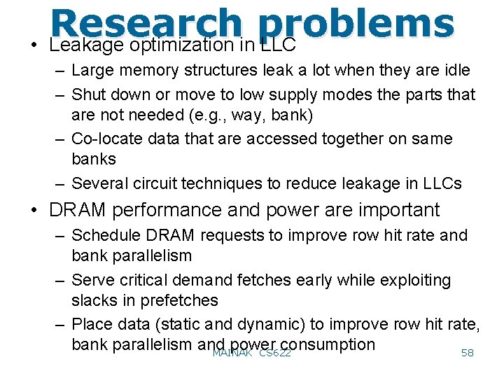
• Research problems Leakage optimization in LLC – Large memory structures leak a lot when they are idle – Shut down or move to low supply modes the parts that are not needed (e. g. , way, bank) – Co-locate data that are accessed together on same banks – Several circuit techniques to reduce leakage in LLCs • DRAM performance and power are important – Schedule DRAM requests to improve row hit rate and bank parallelism – Serve critical demand fetches early while exploiting slacks in prefetches – Place data (static and dynamic) to improve row hit rate, bank parallelism and power consumption 58 MAINAK CS 622

Research problems • Mother of all problems: data delivery to ALUs – Long list of already existing techniques; a sampling: – – – – Criticality-aware instruction scheduler Large instruction window processors Load value prediction Cache hierarchy optimization including compression Interconnect and coherence protocol optimizations Prefetching Checkpoint assisted acceleration Memory access scheduling Computing in memory controller Better DRAM technology and better layout of DRAM bits Computing/Processing in memory including compression Better I/O scheduling and prefetching in NVM, NV storage Compiler optimizations (instruction scheduling, data layout) – Can you add a new bullet to this list? 59

Research problems • Secure memory system – New attacks and new defense mechanisms • Cache attacks and defense • DRAM attacks and defense 60

• Research practices Empirical in nature – Any theoretical model amenable to mathematical treatment needs to make unreasonable assumptions as the underlying interactions are fairly complicated • Experiments are done on a detailed carefully designed processor simulator (written in HLL) – Benchmark applications are run on the simulator to gather execution statistics – Often simulating a full application takes unreasonably large amount of time; representative regions of the application are selected for simulation • One possible selection procedure: Sim. Point • Representative regions should be large enough to capture different. MAINAK phase. CS 622 behavior of an application 61

Research practices • Application analysis is always the starting point of any architecture study – Need to know the customer demands before designing a new vehicle – Application bottlenecks are analyzed on the current generation of hardware to decide the features of the next generation hardware – Three ways to analyze an application • Run on a simulator (very slow, but very detailed) • Profile and instrument (medium speed) – May require instrumenting the source code or binary – Does not offer microarchitecture-level details • Use performance counters (fast, slower than native) – Less accurate due to periodic sampling 62

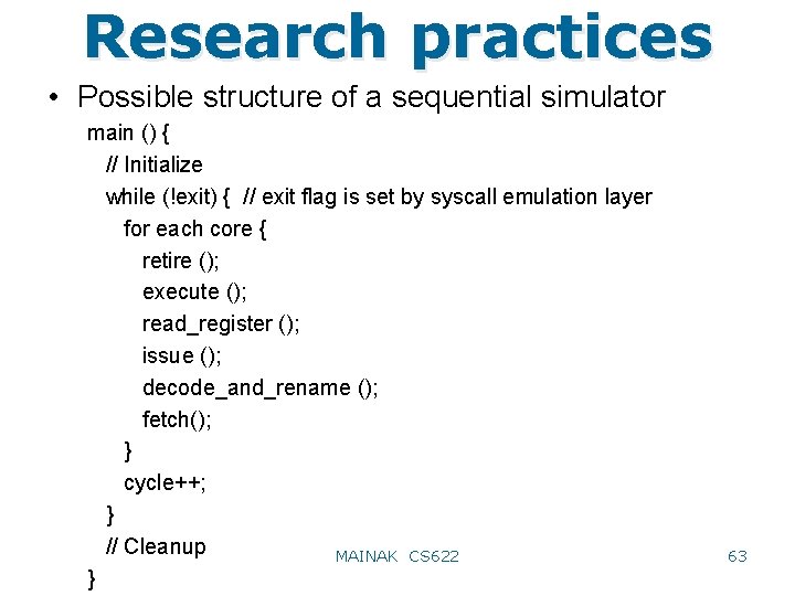
Research practices • Possible structure of a sequential simulator main () { // Initialize while (!exit) { // exit flag is set by syscall emulation layer for each core { retire (); execute (); read_register (); issue (); decode_and_rename (); fetch(); } cycle++; } // Cleanup MAINAK CS 622 } 63

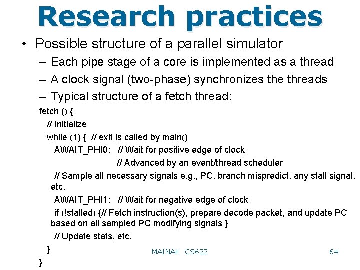
Research practices • Possible structure of a parallel simulator – Each pipe stage of a core is implemented as a thread – A clock signal (two-phase) synchronizes the threads – Typical structure of a fetch thread: fetch () { // Initialize while (1) { // exit is called by main() AWAIT_PHI 0; // Wait for positive edge of clock // Advanced by an event/thread scheduler // Sample all necessary signals e. g. , PC, branch mispredict, any stall signal, etc. AWAIT_PHI 1; // Wait for negative edge of clock if (!stalled) {// Fetch instruction(s), prepare decode packet, and update PC based on all sampled PC modifying signals } // Update stats, etc. } 64 MAINAK CS 622 }

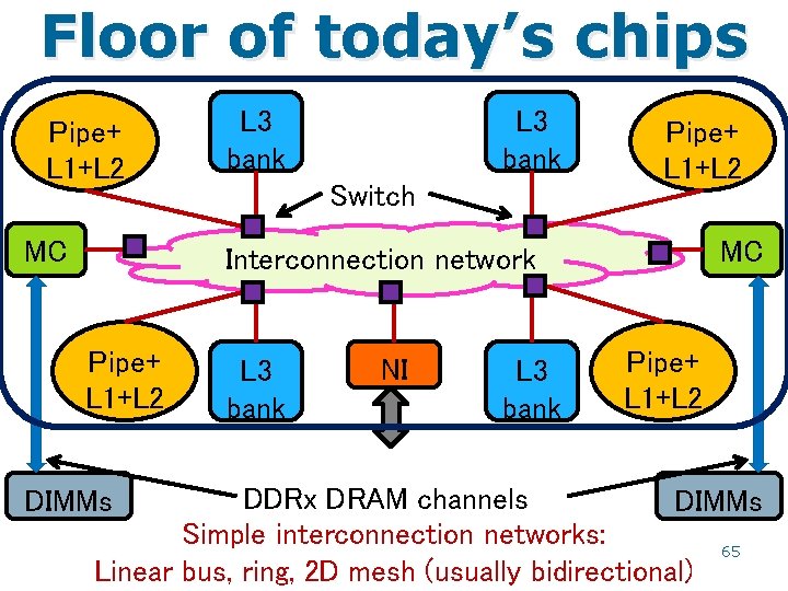
Floor of today’s chips Pipe+ L 1+L 2 MC L 3 bank Switch Pipe+ L 1+L 2 MC Interconnection network Pipe+ L 1+L 2 L 3 bank NI L 3 bank Pipe+ L 1+L 2 DDRx DRAM channels DIMMs Simple interconnection networks: 65 Linear bus, ring, 2 D mesh (usually bidirectional) DIMMs

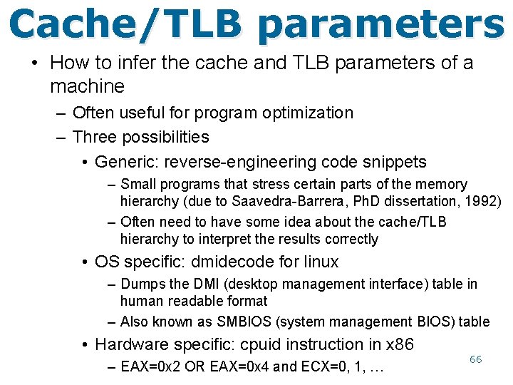
Cache/TLB parameters • How to infer the cache and TLB parameters of a machine – Often useful for program optimization – Three possibilities • Generic: reverse-engineering code snippets – Small programs that stress certain parts of the memory hierarchy (due to Saavedra-Barrera, Ph. D dissertation, 1992) – Often need to have some idea about the cache/TLB hierarchy to interpret the results correctly • OS specific: dmidecode for linux – Dumps the DMI (desktop management interface) table in human readable format – Also known as SMBIOS (system management BIOS) table • Hardware specific: cpuid instruction in x 86 – EAX=0 x 2 OR EAX=0 x 4 and ECX=0, 1, … 66

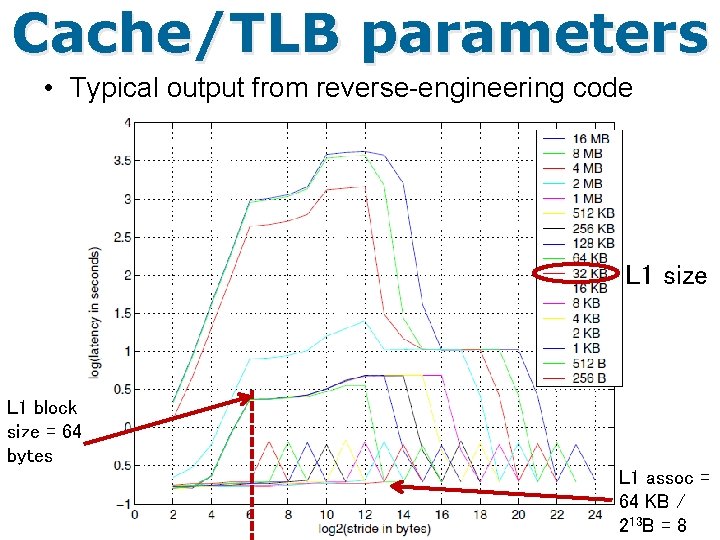
Cache/TLB parameters • Typical output from reverse-engineering code L 1 size L 1 block size = 64 bytes L 1 assoc = 64 KB / 213 B = 8