VHDL signal Counter signal TC signal flop stdlogicvector3


; std_logic; process(Clk) begin if")


; std_logic; process(TC, Clk) begin")
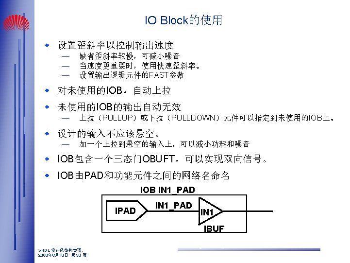
 Counter INPUT D Q 1 Q 0 CLOCK INPUT Counter D TC DATA")
; process(Clk) begin if rising_edge(Clk) then if INPUT=‘")
 Counter INPUT D Q 1 Q 0 CLOCK Async R Counter INPUT D")
; process(Counter, Clk) begin if Counter=“ 11” then")

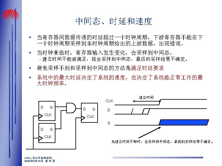
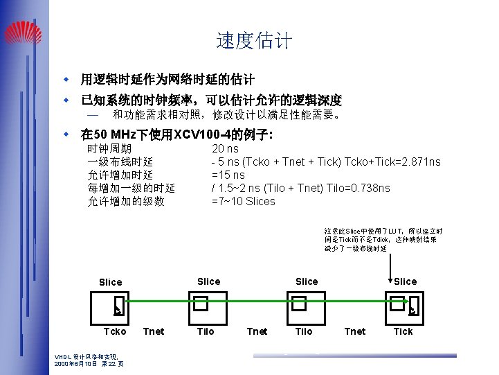
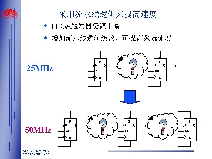
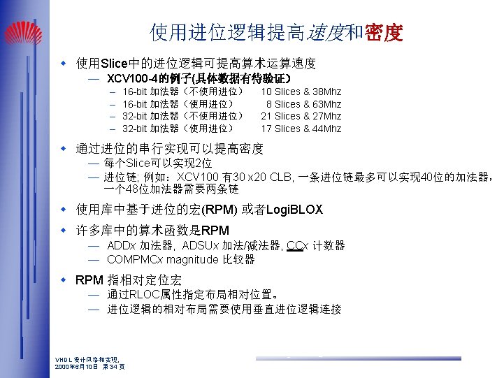

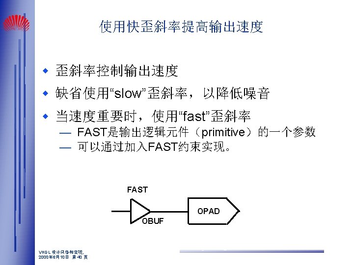
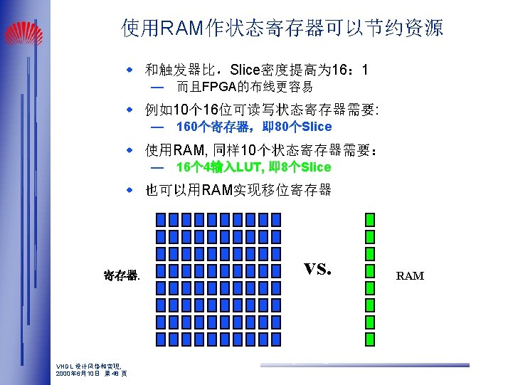
 - Tbrd - Tbufg w 使用“OFFSET")
 发送器(XCV 100 -4 FPGA) D 接收器(XCV 100 -4 FPGA) D Q Q CE")


- Slides: 51
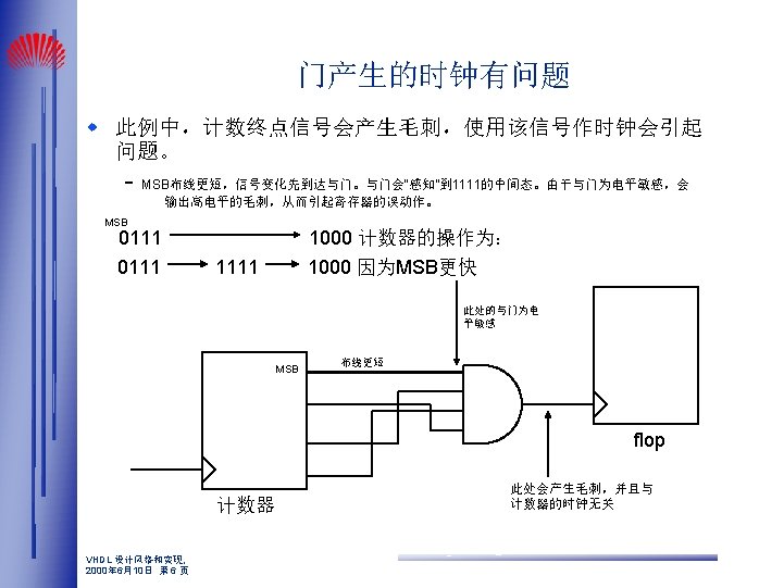
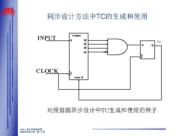
相应的VHDL代码 signal Counter: signal TC: signal flop: std_logic_vector(3 downto 0); std_logic; process(Clk) begin if rising_edge(Clk) then Counter <= Counter + 1; end if; end process; TC <= ‘ 1’ when Counter=“ 1111” else ‘ 0’; process(TC) begin if rising_edge(TC) then flop <= … end if; end process; VHDL 设计风格和实现, 2000年 6月10日 第 7 页 --TC为组合逻辑输出 --使用组合逻辑输出作时钟,是异步设计,禁止!!!
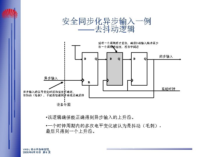
相应的VHDL代码 signal Asyn. Input: signal Input. Reg: signal Delay: signal Syn. Input: std_logic; process(Syn. Input, Asyn. Input) begin if Syn. Input=‘ 1’ then --此置位为寄存器信号,为同步设计,可行 Input. Reg <= ‘ 0’; if rising_edge(Asyn. Input) then Input. Reg <= ‘ 1’; end if; end process; process(Clk) begin if rising_edge(Clk) then Delay <= Input. Reg; Syn. Input <= Delay; end if; VHDL 设计风格和实现, 2000年 6月10日 第 10 页
相应的VHDL代码 signal Counter: signal TC: signal flop: std_logic_vector(3 downto 0); std_logic; process(TC, Clk) begin if TC=‘ 1’ then Counter <= “ 0000”; TC <= ‘-’; elsif rising_edge(Clk) then Counter <= Counter + 1; if Counter=“ 1110” then else end if; end process; VHDL 设计风格和实现, 2000年 6月10日 第 12 页 TC <= ‘ 1’; TC <= ‘ 0’; --此复位为寄存器信号,为同步设计,可行 --注意和异步设计中TC信号的比较 --此处TC为寄存器输出
同步设计的更多例子(可行) Counter INPUT D Q 1 Q 0 CLOCK INPUT Counter D TC DATA D S Q CE CLOCK R VHDL 设计风格和实现, 2000年 6月10日 第 13 页
相应的VHDL代码 例1 signal Counter: std_logic_vector(1 downto 0); process(Clk) begin if rising_edge(Clk) then if INPUT=‘ 1’ and Counter/=“ 11” then Counter <= Counter + 1; end if; --组合逻辑用在寄存器的D端, --为同步设计,可行 end if; end process; 例2 signal Counter: std_logic_vector(3 downto 0); signal TC: std_logic; signal s: std_logic; process(Clk) begin if rising_edge(Clk) then if INPUT=‘ 1’ then Counter <= Counter + 1; end if; if TC=‘ 1’ then --TC 用在寄存器的CE端,为同步设计,可行 s <= DATA; end if; end process; TC <= ‘ 1’ when Counter=“ 1111” else ‘ 0’; --TC为组合逻辑输出 VHDL 设计风格和实现, 2000年 6月10日 第 14 页
异步设计的更多例子(禁止) Counter INPUT D Q 1 Q 0 CLOCK Async R Counter INPUT D TC DATA D S Q CE CLOCK R 这些例子有什么问题 ? VHDL 设计风格和实现, 2000年 6月10日 第 15 页
相应的VHDL代码 例1 signal Counter: std_logic_vector(1 downto 0); process(Counter, Clk) begin if Counter=“ 11” then --组合逻辑用作寄存器的异步复位, --为异步设计,禁止!!! Counter <= “ 00”; elsif rising_edge(Clk) then if INPUT=‘ 1’ then Counter <= Counter + 1; end if; end process; 例2 signal Counter: std_logic_vector(3 downto 0); signal TC: std_logic; signal s: std_logic; process(Clk) begin if rising_edge(Clk) then if INPUT=‘ 1’ then Counter <= Counter + 1; end if; end process; TC <= ‘ 1’ when Counter=“ 1111” else ‘ 0’; --TC为组合逻辑输出 process(TC) begin if rising_edge(TC)=‘ 1’ then --TC 用作寄存器的时钟,为异步设计,禁止! s <= DATA; end if; end process; VHDL 设计风格和实现, 2000年 6月10日 第 16 页
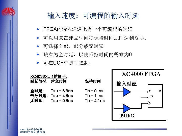
了解进位链流向 w XC 4000 E/L和Spartan/XL进位链流向为上下两个方向 w XC 4000 EX/XL/XV和Virtex器件的进位链流向只能向上 MSB LSB XC 4000 E Spartan/XL VHDL 设计风格和实现, 2000年 6月10日 第 35 页 XC 4000 EX/XL/XV Virtex
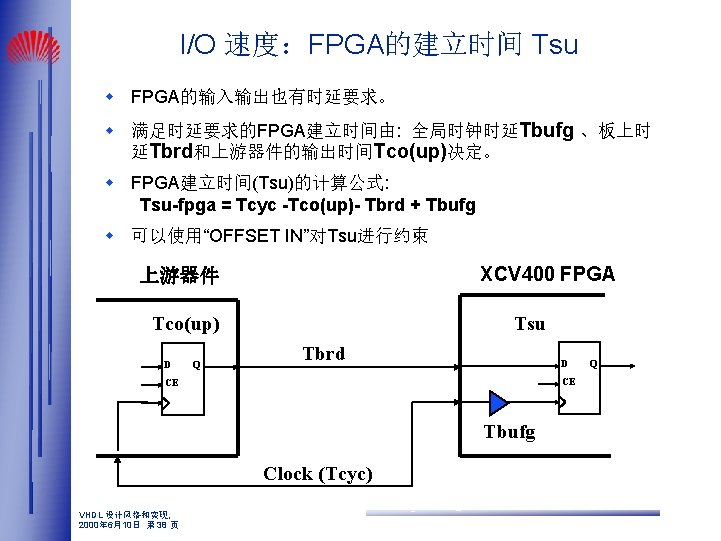
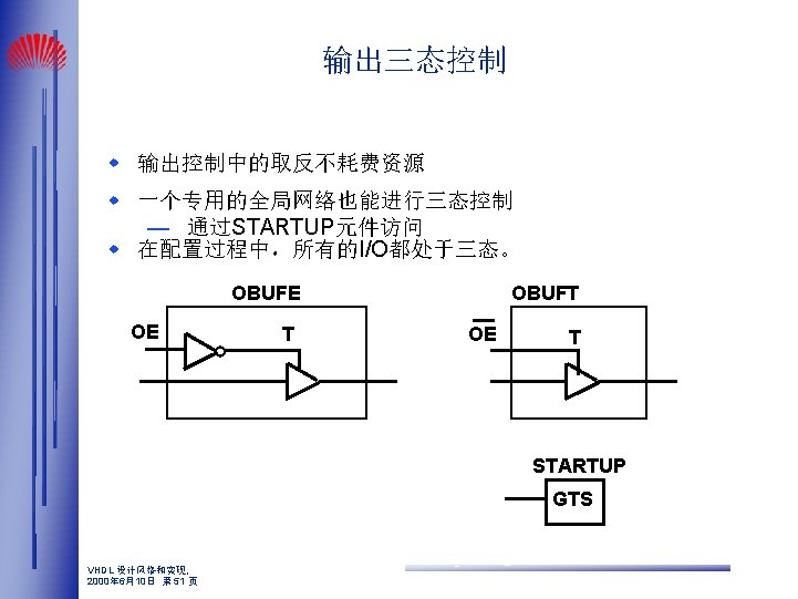
I/O速度:FPGA的输出时间Tco w FPGA输出时间的计算公式: Tco = Tcyc - Tsu(down) - Tbrd - Tbufg w 使用“OFFSET OUT”对Tco进行约束 XCV 400 FPGA 下游器件 Tco Tbufg D Q Tsu(down) Tbrd CE CE Clock (Tcyc) VHDL 设计风格和实现, 2000年 6月10日 第 39 页 D Q
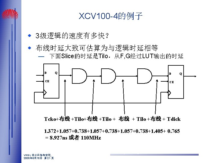
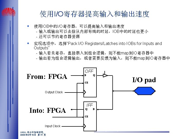
使用I/O寄存器的例子(FPGA-FPGA) 发送器(XCV 100 -4 FPGA) D 接收器(XCV 100 -4 FPGA) D Q Q CE CE 使用IOB中寄存器的时延 Tiockp + PCB网络时延 + Tiopick 5. 649 1. 962 =7. 611 不使用IOB中寄存器的时延 (Tcko + Tnet +Tioop) + PCB网络时延 + (Tiopi + Tnet + Tdick) (1. 372 +0. 756+5. 652) (0. 989+ 1. 930+0. 728) 7. 780 3. 647 =11. 427 VHDL 设计风格和实现, 2000年 6月10日 第 42 页
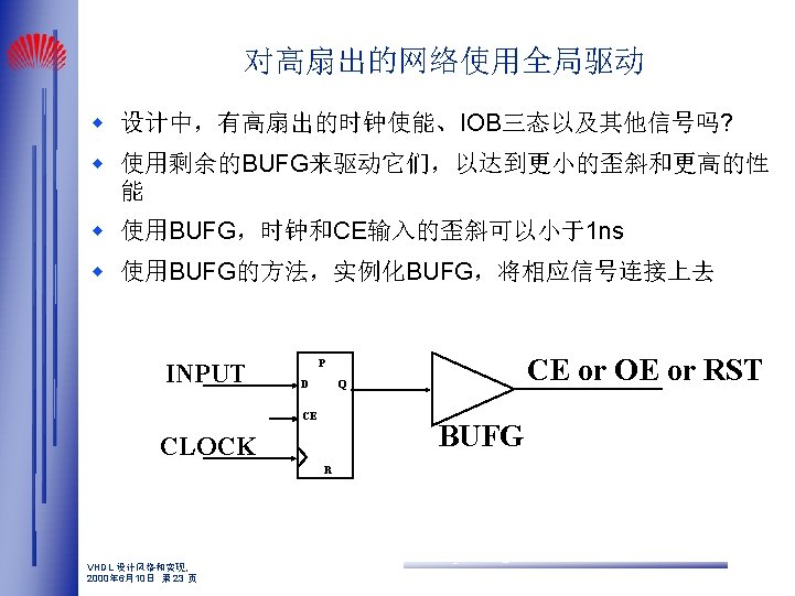
I/O速度的其他提示 w XC 4000 -13, 36, 62 XL是turbo boosted。 w 使用BUFG,可提高pin to pin时延 VHDL 设计风格和实现, 2000年 6月10日 第 44 页
资源估计 w w w 资源使用量是指FPGA使用了的百分率 在宏、库、以及XAPP application notes 中找到可比较的函数来估计资源使用量 — 或者,使用别的设计来估计器件使 用率 快速实现,然后查看MAP报告 Design Summary — 选择“Implementation/ View Report -------Number of errors: 0 Number of warnings: 644 Files/ Map report” Number of Slices: 1, 147 out of 1, 200 95% — Slices, IOBs, Block RAMs, 以及其 Slice Flip Flops: 735 input LUTs: 1, 046 (1 used as a route-thru) 他部件分别列出,并给出使用百分 4 Dual Port RAMs: 312 Number of Slices containing 率。最后给出相当于ASIC的门数 unrelated logic: 0 out of 1, 147 0% Number of bonded IOBs: 85 out of 98 86% IOB Flip Flops: 68 Number of Block RAMs: 10 out of 10 100% Number of GCLKs: 2 out of 4 50% Number of GCLKIOBs: 2 out of 4 50% Number of DLLs: 1 out of 4 25% Number of Startups: 1 out of 1 100% Number of RPM macros: 9 Total equivalent gate count for design: 224, 805 Additional JTAG gate count for IOBs: 4, 176 VHDL 设计风格和实现, 2000年 6月10日 第 46 页