VHDL 8 Practical examples Part 1 7 segment










![The Logic Analyzer • Overall diagram Reset Rec Play DA_in[7. . 0] Xilinx based The Logic Analyzer • Overall diagram Reset Rec Play DA_in[7. . 0] Xilinx based](https://slidetodoc.com/presentation_image/48edf2343602b6ab57c387fe41a957ef/image-47.jpg)




- Slides: 73

VHDL 8 Practical examples Part 1: 7 -segment display , Part 2: A single board sound recorder Part 3: Logic analyzer VHDL 8 Practical example v 8 a 1

Part 1 7 -segment LED display using VHDL 8 Practical example v 8 a 2

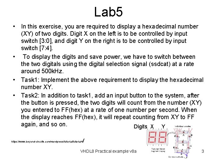
Lab 5 • In this exercise, you are required to display a hexadecimal number (XY) of two digits. Digit X on the left is to be controlled by input switch [3: 0], and digit Y on the right is to be controlled by input switch [7: 4]. • To display the digits and save power, we have to switch between the two digitals using the digital selection signal (ssdcat) at a rate around 500 k. Hz. • Task 1: Implement the above requirement to display the hexadecimal number XY. • Task 2: In addition to task 1, add an input button to the system, after the button is pressed, the two digits will count from the number (XY) you entered to FF(hex) at a rate of one number per second. When the display reaches FF(hex), it will repeat counting from XY to FF again, and so on. Digits X Y https: //www. beyond-circuits. com/wordpress/tutorial 4 / VHDL 8 Practical example v 8 a 3

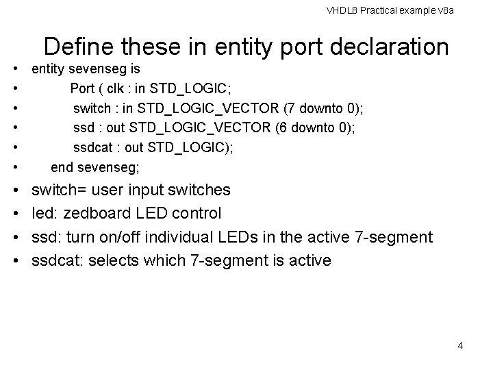
VHDL 8 Practical example v 8 a Define these in entity port declaration • • • entity sevenseg is Port ( clk : in STD_LOGIC; switch : in STD_LOGIC_VECTOR (7 downto 0); ssd : out STD_LOGIC_VECTOR (6 downto 0); ssdcat : out STD_LOGIC); end sevenseg; • • switch= user input switches led: zedboard LED control ssd: turn on/off individual LEDs in the active 7 -segment ssdcat: selects which 7 -segment is active 4

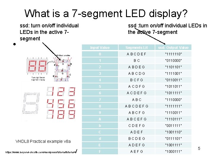
What is a 7 -segment LED display? ssd : turn on/off individual LEDs in the active 7 -segment ssd: turn on/off individual LEDs in the active 7 segment • VHDL 8 Practical example v 8 a https: //www. beyond-circuits. com/wordpress/tutorial 4 / Input Value Segments Lit ssd: Output Value 0 A B C D E F “ 1111110” 1 B C “ 0110000” 2 A B D E G “ 1101101” 3 A B C D G “ 1111001” 4 B C F G “ 0110011” 5 A C D F G “ 1011011” 6 A C D E F G “ 1011111” 7 A B C “ 1110000” 8 A B C D E F G “ 1111111” 9 A B C F G “ 1110011” A A B C E F G “ 1110111” b C D E F G “ 0011111” C A D E F “ 1001110” d B C D E G “ 0111101” E A D E F G “ 1001111” F A E F G “ 1000111” 5

Multiple 7 -segment LED display method • Time multiplexing: – Because LED consumes high power – Make one 7 -segment active at one time will save power. – Activate the 7 -segment on the right then left at a rate of 1 KHz and so on. ssdcat : selects which 7 -segment is active VHDL 8 Practical example v 8 a 6

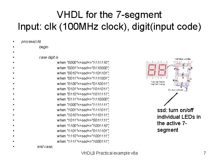
VHDL for the 7 -segment Input: clk (100 MHz clock), digit(input code) • • • • • • process(clk) begin case digit is when "0000"=>ssd<="1111110"; when "0001"=>ssd<="0110000"; when "0010"=>ssd<="1101101"; when "0011"=>ssd<="1111001"; when "0100"=>ssd<="0110011"; when "0101"=>ssd<="1011011"; when "0110"=>ssd<="1011111"; when "0111"=>ssd<="1110000"; when "1000"=>ssd<="1111111"; when "1001"=>ssd<="1111011"; when "1010"=>ssd<="1110111"; when "1011"=>ssd<="0011111"; when "1100"=>ssd<="1001110"; when "1101"=>ssd<="0111101"; when "1110"=>ssd<="1001111"; when "1111"=>ssd<="1000111"; end case; VHDL 8 Practical example v 8 a ssd: turn on/off individual LEDs in the active 7 segment 7

Create a 1 KHz clock from a 100 MHz clk ms_puls e (1 KHz) 0. 5 ms • If the clock frequency of clk is 100 MHz • Create a 1 KHz (or 1 ms-period) clock: ms_pulse • • if rising_edge(clk) then if (count=99999) then ms_pulse <= not ms_pulse; count<=0; else count <= count + 1; end if; 8 end if; VHDL 8 Practical example v 8 a

Select input switches depending on ms_pulse • • • if ms_pulse='1' then digit <= switch(7 downto 4) else digit <= switch(3 downto 0); end if; ssdcat <= ms_pulse; ms_puls e (1 KHz) 0. 5 ms VHDL 8 Practical example v 8 a 9

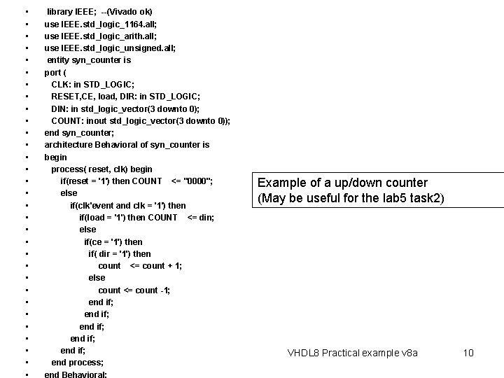
• • • • • • • • library IEEE; --(Vivado ok) use IEEE. std_logic_1164. all; use IEEE. std_logic_arith. all; use IEEE. std_logic_unsigned. all; entity syn_counter is port ( CLK: in STD_LOGIC; RESET, CE, load, DIR: in STD_LOGIC; DIN: in std_logic_vector(3 downto 0); COUNT: inout std_logic_vector(3 downto 0)); end syn_counter; architecture Behavioral of syn_counter is begin process( reset, clk) begin if(reset = '1') then COUNT <= "0000"; else if(clk'event and clk = '1') then if(load = '1') then COUNT <= din; else if(ce = '1') then if( dir = '1') then count <= count + 1; else count <= count -1; end if; end if; end process; end Behavioral; Example of a up/down counter (May be useful for the lab 5 task 2) VHDL 8 Practical example v 8 a 10

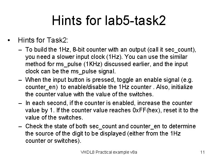
Hints for lab 5 -task 2 • Hints for Task 2: – To build the 1 Hz, 8 -bit counter with an output (call it sec_count), you need a slower input clock (1 Hz). You can use the similar method for ms_pulse (1 KHz) discussed earlier, and the input clock can be the ms_pulse signal. – When the input button is pressed, toggle an enable signal (e. g. counter_en) to enable/disable the 1 Hz counter. Also, initialize the counter value with the value of the switches. – In each second, if the counter is enabled, increase the counter value by 1. If the counter value reaches 0 x. FF(hex), reset it to the value of the switches. – Check the state of both sec_count and counter_en to determine the source of the digit to be displayed (either from the 1 Hz counter or switches). VHDL 8 Practical example v 8 a 11

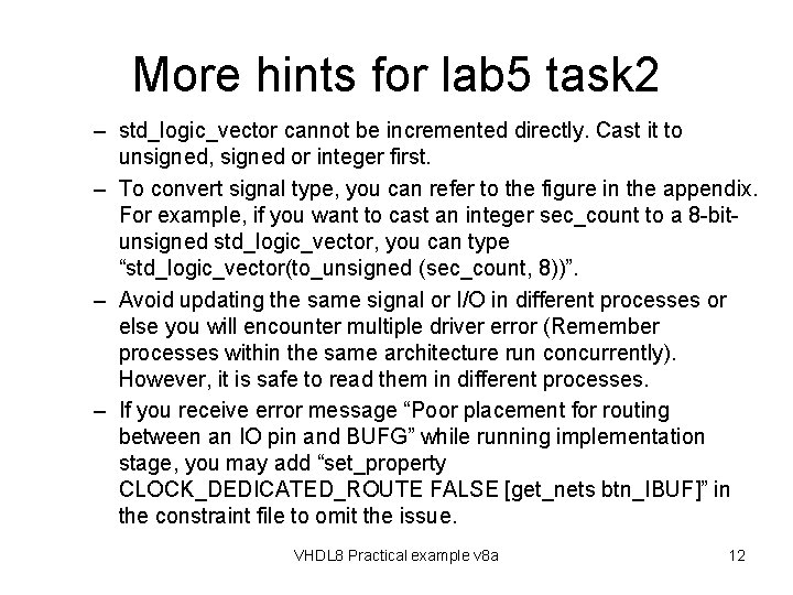
More hints for lab 5 task 2 – std_logic_vector cannot be incremented directly. Cast it to unsigned, signed or integer first. – To convert signal type, you can refer to the figure in the appendix. For example, if you want to cast an integer sec_count to a 8 -bitunsigned std_logic_vector, you can type “std_logic_vector(to_unsigned (sec_count, 8))”. – Avoid updating the same signal or I/O in different processes or else you will encounter multiple driver error (Remember processes within the same architecture run concurrently). However, it is safe to read them in different processes. – If you receive error message “Poor placement for routing between an IO pin and BUFG” while running implementation stage, you may add “set_property CLOCK_DEDICATED_ROUTE FALSE [get_nets btn_IBUF]” in the constraint file to omit the issue. VHDL 8 Practical example v 8 a 12

Part 2 General concept of memory VHDL 8 Practical example v 8 a 13

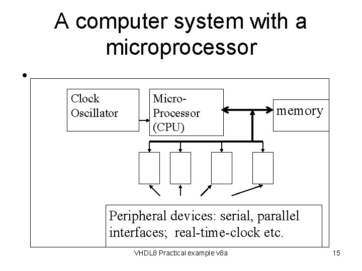
Basic structure of a microprocessor system • • CPU Memory Input/output and peripheral devices Glue logic circuits VHDL 8 Practical example v 8 a 14

A computer system with a microprocessor • Clock Oscillator Micro. Processor (CPU) memory Peripheral devices: serial, parallel interfaces; real-time-clock etc. VHDL 8 Practical example v 8 a 15

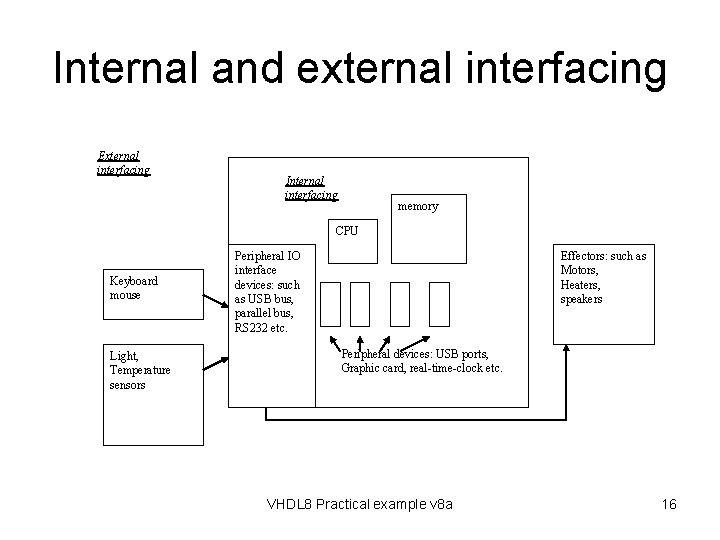
Internal and external interfacing External interfacing Internal interfacing memory CPU Keyboard mouse Light, Temperature sensors Peripheral IO interface devices: such as USB bus, parallel bus, RS 232 etc. Effectors: such as Motors, Heaters, speakers Peripheral devices: USB ports, Graphic card, real-time-clock etc. VHDL 8 Practical example v 8 a 16

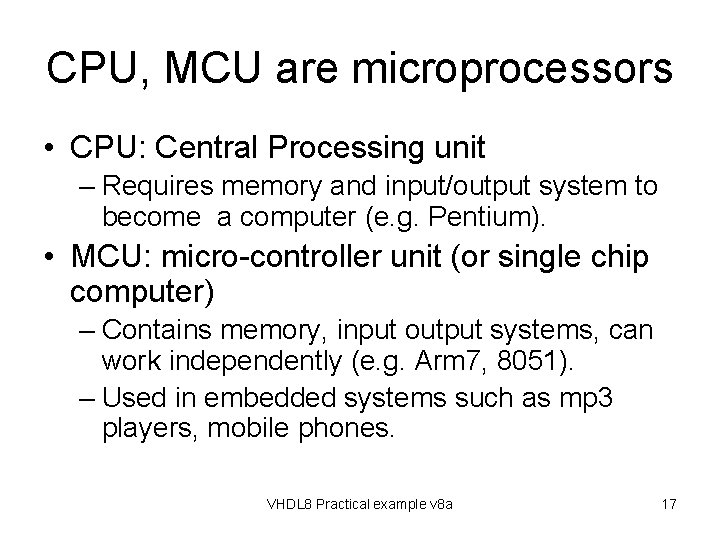
CPU, MCU are microprocessors • CPU: Central Processing unit – Requires memory and input/output system to become a computer (e. g. Pentium). • MCU: micro-controller unit (or single chip computer) – Contains memory, input output systems, can work independently (e. g. Arm 7, 8051). – Used in embedded systems such as mp 3 players, mobile phones. VHDL 8 Practical example v 8 a 17

Memory systems RAM/ROM VHDL 8 Practical example v 8 a 18

Different kinds of Memory (RAM) • Random access memory (RAM): data will disappear after power down. – Static RAM (SRAM): each bit is a flip-flop – Dynamic RAM (DRAM): each bit is a small capacitor, and is needed to be recharged regularly • Since we only discuss static (SRAM) here, so the terms SRAM and RAM will be used interchangeably. VHDL 8 Practical example v 8 a 19

Different kinds of Memory (ROM) • Read only memory (ROM) – UV-EPROM – EEPROM – FLASH ROM VHDL 8 Practical example v 8 a 20

UV-EPROM • VHDL 8 Practical example v 8 a 21

• Flash memory Or SD (secure digital card) http: //videoengineer. net/images/sdc 32 g 2. jpg VHDL 8 Practical example v 8 a 22

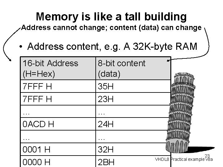
Memory is like a tall building Address cannot change; content (data) can change • Address content, e. g. A 32 K-byte RAM 16 -bit Address (H=Hex) 7 FFF H … 0 ACD H … 0001 H 0000 H 8 -bit content (data) 35 H 23 H … 24 H … 32 H 2 BH 23 VHDL 8 Practical example v 8 a

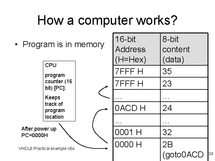
How a computer works? • Program is in memory CPU program counter (16 bit) [PC]: Keeps track of program location After power up PC=0000 H VHDL 8 Practical example v 8 a 16 -bit Address (H=Hex) 7 FFF H … 0 ACD H … 0001 H 0000 H 8 -bit content (data) 35 23 … 24 … 32 2 B (goto 0 ACD 24

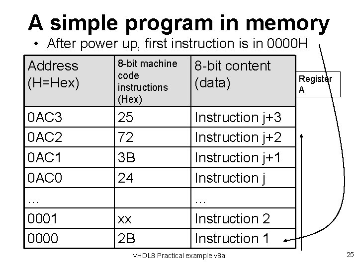
A simple program in memory • After power up, first instruction is in 0000 H • An example 8 -bit machine 8 -bit content Address code Register (H=Hex) (data) instructions A (Hex) 0 AC 3 0 AC 2 0 AC 1 0 AC 0 … 0001 0000 25 72 3 B 24 xx 2 B Instruction j+3 Instruction j+2 Instruction j+1 Instruction j … Instruction 2 Instruction 1 VHDL 8 Practical example v 8 a 25

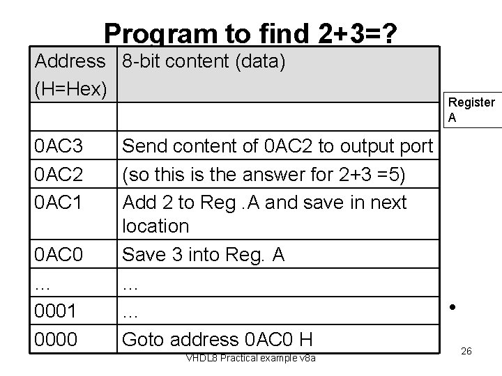
Program to find 2+3=? Address 8 -bit content (data) (H=Hex) 0 AC 3 0 AC 2 0 AC 1 0 AC 0 … 0001 0000 Register A Send content of 0 AC 2 to output port (so this is the answer for 2+3 =5) Add 2 to Reg. A and save in next location Save 3 into Reg. A … • … Goto address 0 AC 0 H 26 VHDL 8 Practical example v 8 a

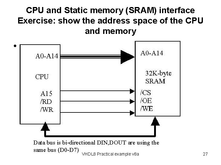
CPU and Static memory (SRAM) interface Exercise: show the address space of the CPU and memory • Data bus is bi-directional DIN, DOUT are using the same bus (D 0 -D 7) VHDL 8 Practical example v 8 a 27

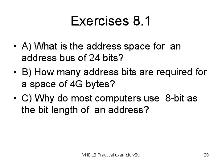
Exercises 8. 1 • A) What is the address space for an address bus of 24 bits? • B) How many address bits are required for a space of 4 G bytes? • C) Why do most computers use 8 -bit as the bit length of an address? VHDL 8 Practical example v 8 a 28

Memory read/write Timing diagrams http: //www. alliancememory. com/pdf/AS 6 C 62256. pdf VHDL 8 Practical example v 8 a 29

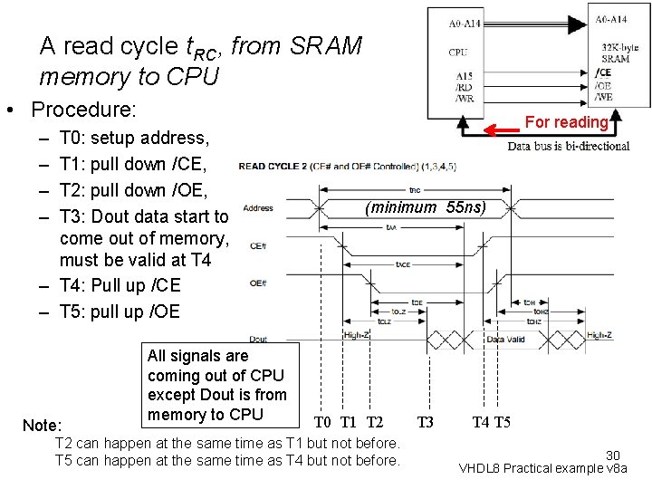
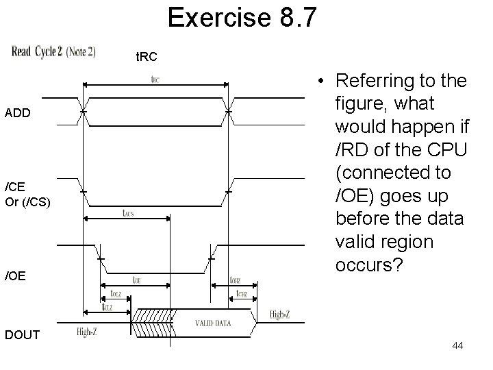
A read cycle t. RC, from SRAM memory to CPU • Procedure: – – T 0: setup address, T 1: pull down /CE, T 2: pull down /OE, T 3: Dout data start to come out of memory, must be valid at T 4 – T 4: Pull up /CE – T 5: pull up /OE Note: All signals are coming out of CPU except Dout is from memory to CPU For reading (minimum 55 ns) T 0 T 1 T 2 can happen at the same time as T 1 but not before. T 5 can happen at the same time as T 4 but not before. T 3 T 4 T 5 30 VHDL 8 Practical example v 8 a

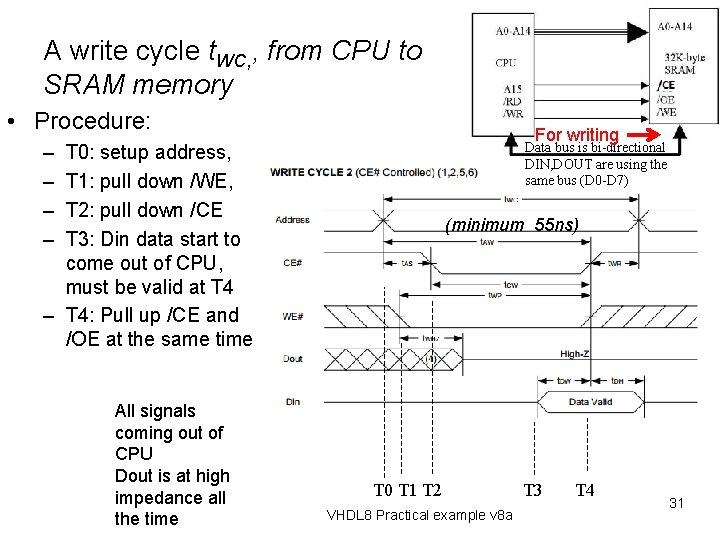
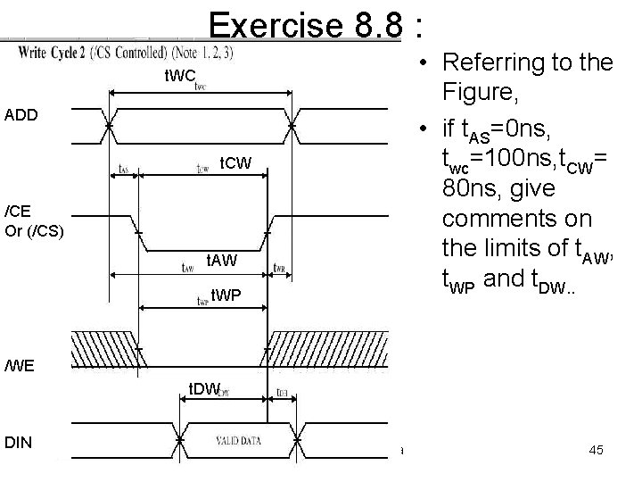
A write cycle t. WC, , from CPU to SRAM memory • Procedure: For writing Data bus is bi-directional DIN, DOUT the Data busareis using bi-directional same. DIN, DOUT bus (D 0 -D 7)are using the – – T 0: setup address, T 1: pull down /WE, T 2: pull down /CE T 3: Din data start to come out of CPU, must be valid at T 4 – T 4: Pull up /CE and /OE at the same time All signals coming out of CPU Dout is at high impedance all the time same bus (D 0 -D 7) (minimum 55 ns) T 0 T 1 T 2 VHDL 8 Practical example v 8 a T 3 T 4 31

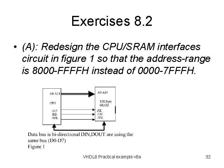
Exercises 8. 2 • (A): Redesign the CPU/SRAM interfaces circuit in figure 1 so that the address-range is 8000 -FFFFH instead of 0000 -7 FFFH. VHDL 8 Practical example v 8 a 32

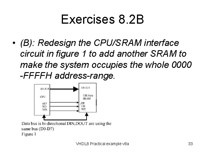
Exercises 8. 2 B • (B): Redesign the CPU/SRAM interface circuit in figure 1 to add another SRAM to make the system occupies the whole 0000 -FFFFH address-range. VHDL 8 Practical example v 8 a 33

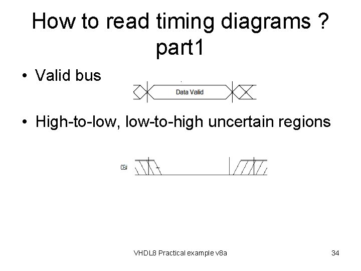
How to read timing diagrams ? part 1 • Valid bus • High-to-low, low-to-high uncertain regions VHDL 8 Practical example v 8 a 34

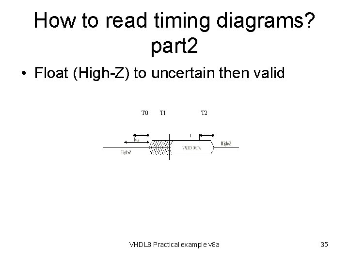
How to read timing diagrams? part 2 • Float (High-Z) to uncertain then valid T 0 T 1 T 2 VHDL 8 Practical example v 8 a 35

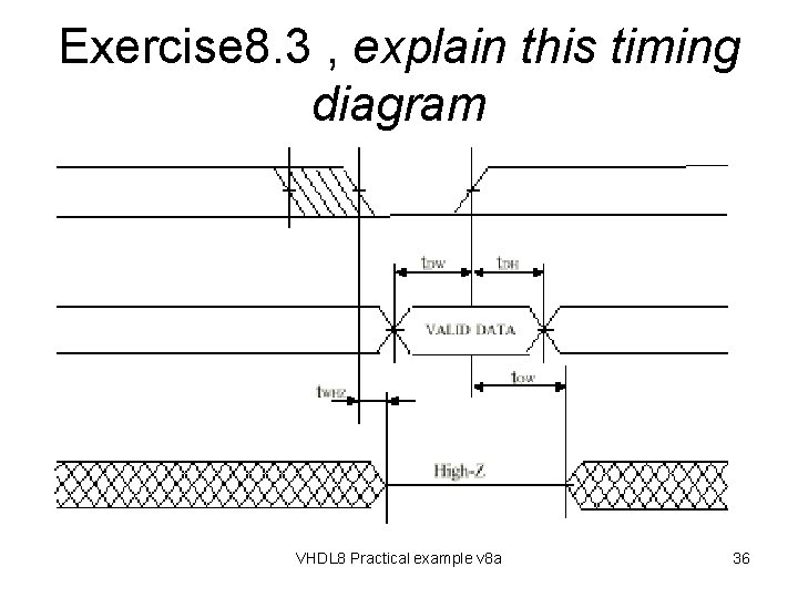
Exercise 8. 3 , explain this timing diagram VHDL 8 Practical example v 8 a 36

Address decoding VHDL 8 Practical example v 8 a 37

Exercises 8. 4 • A CPU supports 128 K-byte (has address pin A 0 -A 16 = 17 pins, so 217=128 K) of memory area. • Exercise 2. 4: How many 32 K-SRAMs do we need? VHDL 8 Practical example v 8 a 38

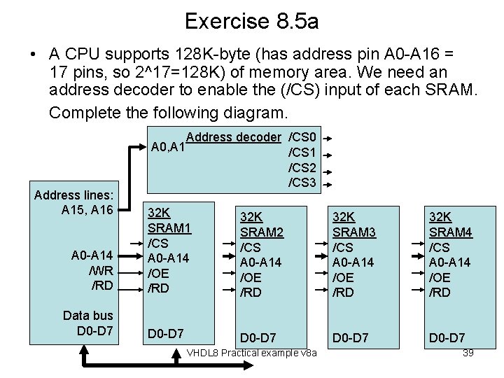
Exercise 8. 5 a • A CPU supports 128 K-byte (has address pin A 0 -A 16 = 17 pins, so 2^17=128 K) of memory area. We need an address decoder to enable the (/CS) input of each SRAM. Complete the following diagram. A 0, A 1 Address lines: A 15, A 16 A 0 -A 14 /WR /RD Data bus D 0 -D 7 Address decoder /CS 0 /CS 1 /CS 2 /CS 3 32 K SRAM 1 /CS A 0 -A 14 /OE /RD 32 K SRAM 2 /CS A 0 -A 14 /OE /RD 32 K SRAM 3 /CS A 0 -A 14 /OE /RD 32 K SRAM 4 /CS A 0 -A 14 /OE /RD D 0 -D 7 VHDL 8 Practical example v 8 a 39

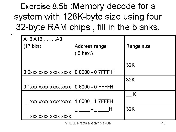
Exercise 8. 5 b : Memory decode for a system with 128 K-byte size using four 32 -byte RAM chips , fill in the blanks. • A 16, A 15, ……. . A 0 (17 bits) Address range ( 5 hex. ) Range size 32 K 0 0 xxx xxxx 0 0000 - 0 7 FFF H 32 K 0 1 xxx xxxx 0 8000 - 0 FFFFH __ K _ _xxx xxxx 1 0000 - 1 7 FFFH _ ____ - _ ____H 32 K 1 1 xxx xxxx VHDL 8 Practical example v 8 a 40

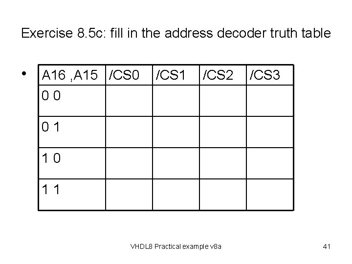
Exercise 8. 5 c: fill in the address decoder truth table • A 16 , A 15 /CS 0 /CS 1 /CS 2 /CS 3 0 0 0 1 1 VHDL 8 Practical example v 8 a 41

Address decode rules • Decode the upper address lines using a decoder. • Connect lower address lines directly to memory devices. VHDL 8 Practical example v 8 a 42

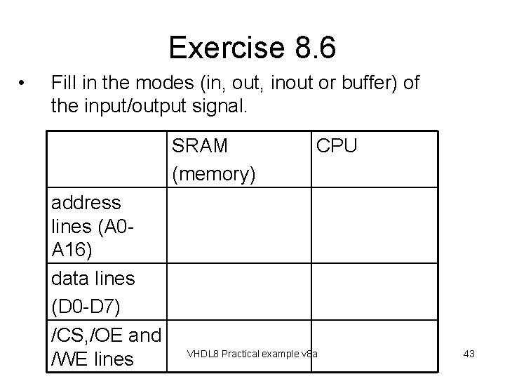
Exercise 8. 6 • Fill in the modes (in, out, inout or buffer) of the input/output signal. SRAM (memory) address lines (A 0 A 16) data lines (D 0 -D 7) /CS, /OE and /WE lines CPU VHDL 8 Practical example v 8 a 43

Exercise 8. 7 t. RC • Referring to the figure, what would happen if /RD of the CPU (connected to /OE) goes up before the data valid region occurs? ADD /CE Or (/CS) /OE DOUT VHDL 8 Practical example v 8 a 44

Exercise 8. 8 : t. WC ADD t. CW /CE Or (/CS) t. AW t. WP • Referring to the Figure, • if t. AS=0 ns, twc=100 ns, t. CW= 80 ns, give comments on the limits of t. AW, t. WP and t. DW. . /WE t. DW DIN VHDL 8 Practical example v 8 a 45

Part 3 The Logic Analyzer VHDL 8 Practical example v 8 a 46
![The Logic Analyzer Overall diagram Reset Rec Play DAin7 0 Xilinx based The Logic Analyzer • Overall diagram Reset Rec Play DA_in[7. . 0] Xilinx based](https://slidetodoc.com/presentation_image/48edf2343602b6ab57c387fe41a957ef/image-47.jpg)
The Logic Analyzer • Overall diagram Reset Rec Play DA_in[7. . 0] Xilinx based hardware DA_out[7. . 0] Serial ARM 7 port board Display waveform RAM VHDL 8 Practical example v 8 a 47

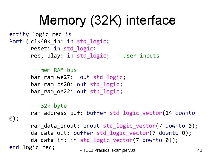
Memory (32 K) interface entity logic_rec is Port ( clk 40 k_in: in std_logic; reset: in std_logic; rec, play: in std_logic; --user inputs -- mem RAM bus bar_ram_we 27: out std_logic; bar_ram_cs 20: out std_logic; bar_ram_oe 22: out std_logic; 0); -- 32 k-byte ram_address_buf: buffer std_logic_vector(14 downto ram_data_inout: inout std_logic_vector(7 downto 0); da_data_out: buffer std_logic_vector(7 downto 0); da_data_in: in std_logic_vector(7 downto 0)); end logic_rec; VHDL 8 Practical example v 8 a 48

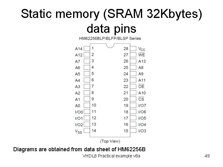
Static memory (SRAM 32 Kbytes) data pins Diagrams are obtained from data sheet of HM 62256 B VHDL 8 Practical example v 8 a 49

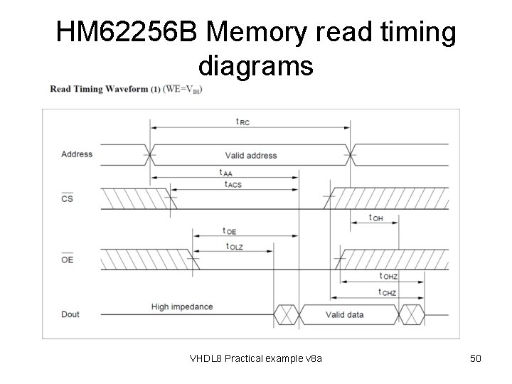
HM 62256 B Memory read timing diagrams VHDL 8 Practical example v 8 a 50

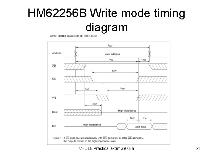
HM 62256 B Write mode timing diagram VHDL 8 Practical example v 8 a 51

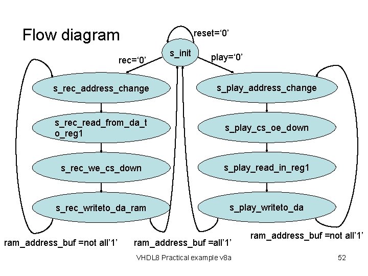
Flow diagram reset=‘ 0’ rec=‘ 0’ s_init play=‘ 0’ s_rec_address_change s_play_address_change s_rec_read_from_da_t o_reg 1 s_play_cs_oe_down s_rec_we_cs_down s_play_read_in_reg 1 s_rec_writeto_da_ram s_play_writeto_da ram_address_buf =not all’ 1’ ram_address_buf =all’ 1’ VHDL 8 Practical example v 8 a ram_address_buf =not all’ 1’ 52

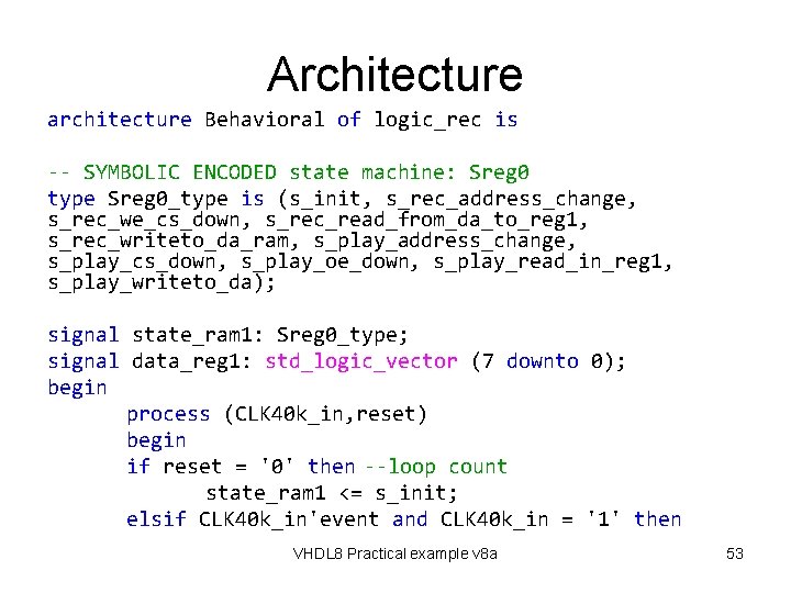
Architecture architecture Behavioral of logic_rec is -- SYMBOLIC ENCODED state machine: Sreg 0 type Sreg 0_type is (s_init, s_rec_address_change, s_rec_we_cs_down, s_rec_read_from_da_to_reg 1, s_rec_writeto_da_ram, s_play_address_change, s_play_cs_down, s_play_oe_down, s_play_read_in_reg 1, s_play_writeto_da); signal state_ram 1: Sreg 0_type; signal data_reg 1: std_logic_vector (7 downto 0); begin process (CLK 40 k_in, reset) begin if reset = '0' then --loop count state_ram 1 <= s_init; elsif CLK 40 k_in'event and CLK 40 k_in = '1' then VHDL 8 Practical example v 8 a 53

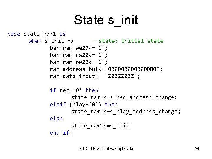
State s_init case state_ram 1 is when s_init => --state: initial state bar_ram_we 27<='1'; bar_ram_cs 20<='1'; bar_ram_oe 22<='1'; ram_address_buf<="00000000"; ram_data_inout<= "ZZZZ"; if rec='0' then state_ram 1<=s_rec_address_change; elsif (play='0') then state_ram 1<=s_play_address_change; else state_ram 1<=s_init; end if; VHDL 8 Practical example v 8 a 54

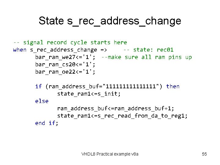
State s_rec_address_change -- signal record cycle starts here when s_rec_address_change => -- state: rec 01 bar_ram_we 27<='1'; --make sure all ram pins up bar_ram_cs 20<='1'; bar_ram_oe 22<='1'; if (ram_address_buf="11111111") then state_ram 1<=s_init; else ram_address_buf<=ram_address_buf+1; state_ram 1<=s_rec_read_from_da_to_reg 1; end if; VHDL 8 Practical example v 8 a 55

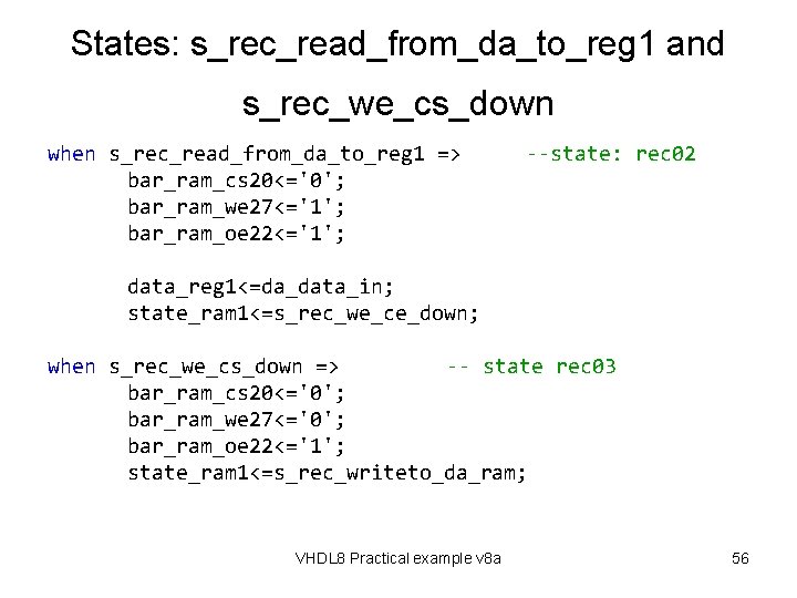
States: s_rec_read_from_da_to_reg 1 and s_rec_we_cs_down when s_rec_read_from_da_to_reg 1 => bar_ram_cs 20<='0'; bar_ram_we 27<='1'; bar_ram_oe 22<='1'; --state: rec 02 data_reg 1<=da_data_in; state_ram 1<=s_rec_we_ce_down; when s_rec_we_cs_down => -- state rec 03 bar_ram_cs 20<='0'; bar_ram_we 27<='0'; bar_ram_oe 22<='1'; state_ram 1<=s_rec_writeto_da_ram; VHDL 8 Practical example v 8 a 56

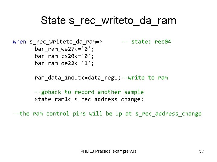
State s_rec_writeto_da_ram when s_rec_writeto_da_ram=> bar_ram_we 27<='0'; bar_ram_cs 20<='0'; bar_ram_oe 22<='1'; -- state: rec 04 ram_data_inout<=data_reg 1; --write to ram --goback to record another sample state_ram 1<=s_rec_address_change; --the ram control pins will be up at s_rec_address_change VHDL 8 Practical example v 8 a 57

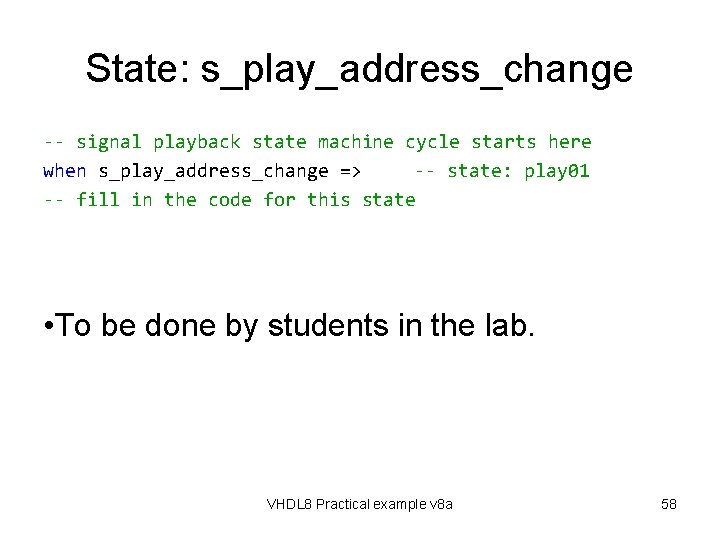
State: s_play_address_change -- signal playback state machine cycle starts here when s_play_address_change => -- state: play 01 -- fill in the code for this state • To be done by students in the lab. VHDL 8 Practical example v 8 a 58

Conclusion • Showed how to make a single board logic analyzer by VHDL • Can be modified for sound recorder, digital camera, mp 3 player etc. VHDL 8 Practical example v 8 a 59

Bonus Part Using a FIFO (first in first out) memory VHDL 8 Practical example v 8 a 60

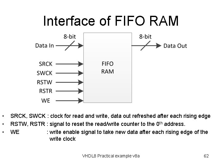
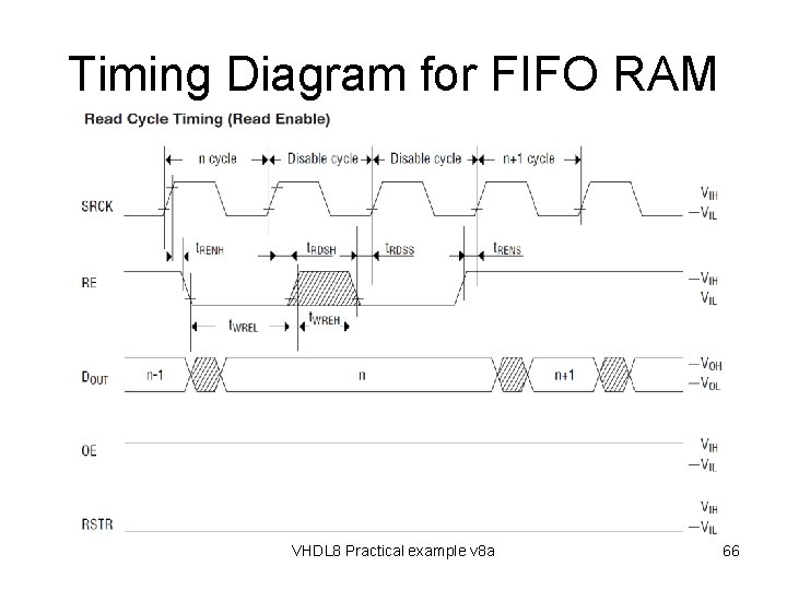
FIFO RAM • Very similar to the previously introduced SRAM. • It has an internal counter to ensure the data are read and written in FIFO manner. • No need to specify address. VHDL 8 Practical example v 8 a 61

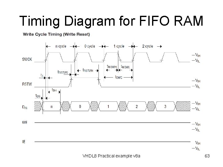
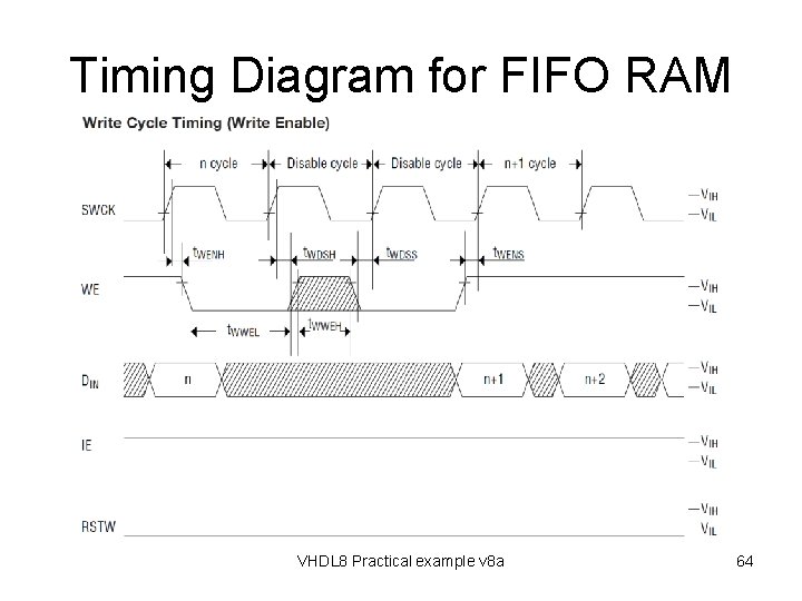
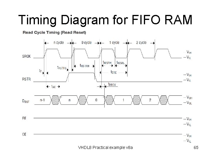
Interface of FIFO RAM • • • SRCK, SWCK : clock for read and write, data out refreshed after each rising edge RSTW, RSTR : signal to reset the read/write counter to the 0 th address. WE : write enable signal to take new data after each rising edge of the write clock VHDL 8 Practical example v 8 a 62

Timing Diagram for FIFO RAM VHDL 8 Practical example v 8 a 63

Timing Diagram for FIFO RAM VHDL 8 Practical example v 8 a 64

Timing Diagram for FIFO RAM VHDL 8 Practical example v 8 a 65

Timing Diagram for FIFO RAM VHDL 8 Practical example v 8 a 66

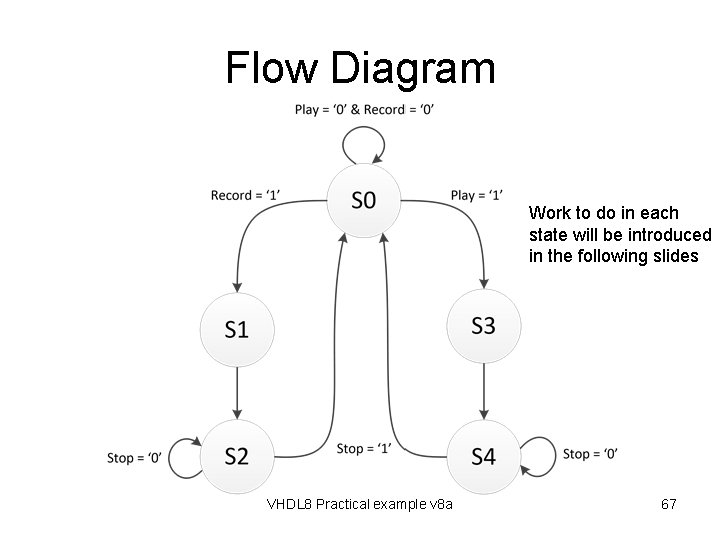
Flow Diagram Work to do in each state will be introduced in the following slides VHDL 8 Practical example v 8 a 67

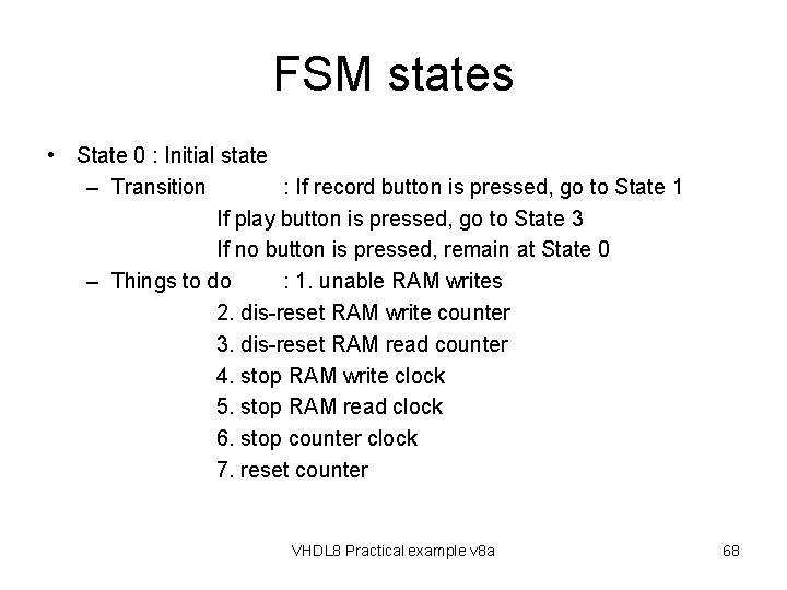
FSM states • State 0 : Initial state – Transition : If record button is pressed, go to State 1 If play button is pressed, go to State 3 If no button is pressed, remain at State 0 – Things to do : 1. unable RAM writes 2. dis-reset RAM write counter 3. dis-reset RAM read counter 4. stop RAM write clock 5. stop RAM read clock 6. stop counter clock 7. reset counter VHDL 8 Practical example v 8 a 68

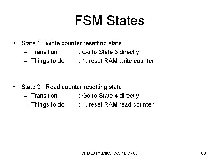
FSM States • State 1 : Write counter resetting state – Transition : Go to State 3 directly – Things to do : 1. reset RAM write counter • State 3 : Read counter resetting state – Transition : Go to State 4 directly – Things to do : 1. reset RAM read counter VHDL 8 Practical example v 8 a 69

FSM States • State 2 : Record state – Transition : If stop signal is high, go to state 0 else remain at state 2 – Things to do : 1. enable RAM writes 2. start RAM write clock 3. stop RAM read clock 4. start counter clock 5. dis-reset counter 6. dis-reset RAM write counter VHDL 8 Practical example v 8 a 70

FSM States • State 4 : Play state – Transition : If stop signal is high, go to state 0 else remain at state 4 – Things to do : 1. disable RAM writes 2. stop RAM write clock 3. start RAM read clock 4. start counter clock 5. dis-reset counter 6. dis-reset RAM read counter VHDL 8 Practical example v 8 a 71

Sound Recorder utilizing FIFO RAM • To be done in the lab. • A full skeleton code is given but need to fill in missing part in the FSM. VHDL 8 Practical example v 8 a 72

Conclusion • Showed how to make a single board sound recorder by VHDL • Can be modified for digital camera, mp 3 player etc. VHDL 8 Practical example v 8 a 73