VFET A Transistor Structure for Amorphous semiconductors Michael
![Processes - Blockcopolymers Annealing Disordered to molecularly organized Thermal annealing [T↑, TG const. ] Processes - Blockcopolymers Annealing Disordered to molecularly organized Thermal annealing [T↑, TG const. ]](https://slidetodoc.com/presentation_image_h2/aac86efb07454791a0aa003f45c051df/image-6.jpg)

- Slides: 25

VFET – A Transistor Structure for Amorphous semiconductors Michael Greenman, Ariel Ben-Sasson, Nir Tessler Sara and Moshe Zisapel Nano-Electronic Center, EE Dept. , Technion Israel Institute of Technology, Haifa, Israel

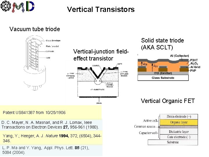
III Vertical Transistors Vacuum tube triode Vertical-junction fieldeffect transistor Solid state triode (AKA SCLT) Vertical Organic FET Patent US 841387 from 10/25/1906 D. C. Mayer, N. A. Masnari, and R. J. Lomax, Ieee Transactions on Electron Devices 27, 956 -961 (1980). Yang, Y. ; Heeger, A. J. Nature 1994, 372, (6504), 344346. L. P. Ma and Y. Yang, Appl. Phys. Lett. 85 (21), 5084 (2004).

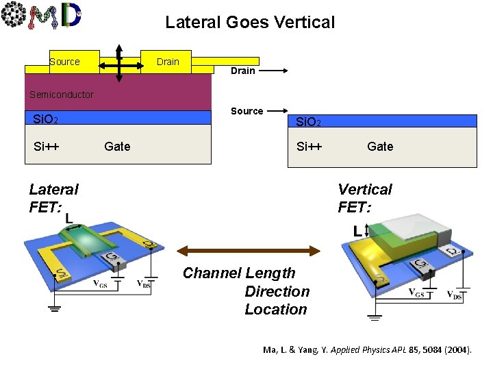
Lateral Goes Vertical Source L Drain Semiconductor Source Si. O 2 Si++ Gate Si. O 2 Si++ Lateral FET: Gate Vertical FET: Channel Length Direction Location Ma, L. & Yang, Y. Applied Physics APL 85, 5084 (2004).

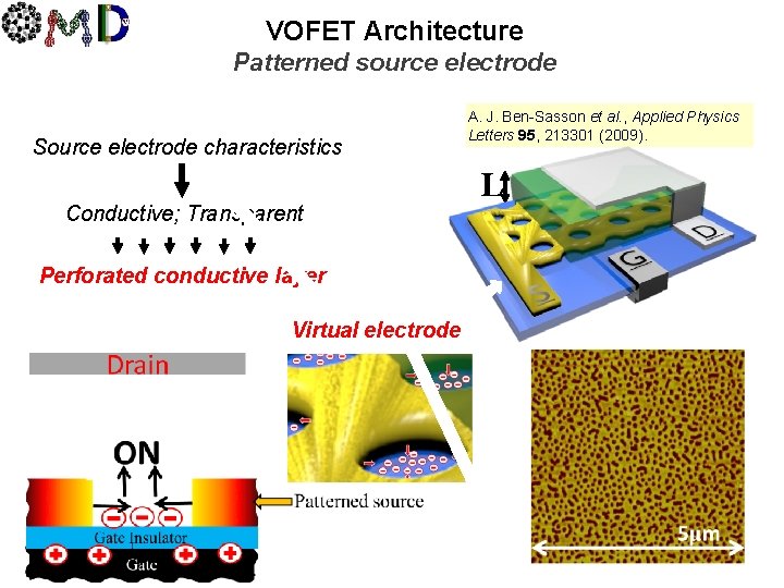
III VOFET Architecture Patterned source electrode Source electrode characteristics Conductive; Transparent Perforated conductive layer Virtual electrode A. J. Ben-Sasson et al. , Applied Physics Letters 95, 213301 (2009). L

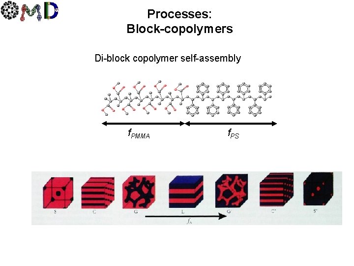
Processes: Block-copolymers Di-block copolymer self-assembly f. PMMA f. PS
![Processes Blockcopolymers Annealing Disordered to molecularly organized Thermal annealing T TG const Processes - Blockcopolymers Annealing Disordered to molecularly organized Thermal annealing [T↑, TG const. ]](https://slidetodoc.com/presentation_image_h2/aac86efb07454791a0aa003f45c051df/image-6.jpg)
Processes - Blockcopolymers Annealing Disordered to molecularly organized Thermal annealing [T↑, TG const. ] Solvent annealing [T const. , TG↓] 3µm

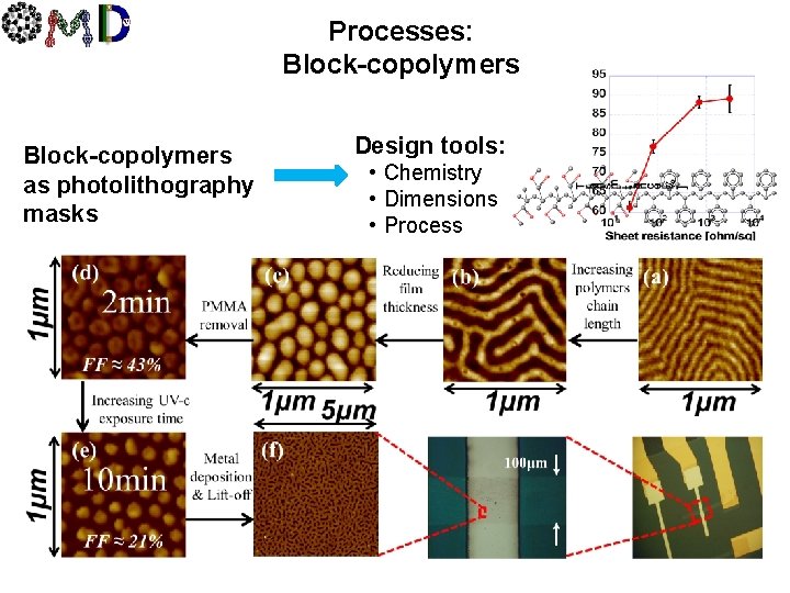
IV Block-copolymers as photolithography masks Processes: Block-copolymers Design tools: • Chemistry • Dimensions • Process

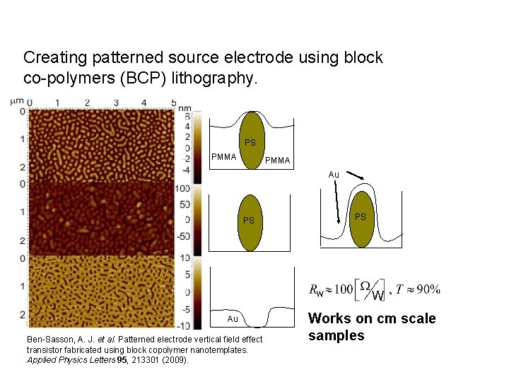
Creating patterned source electrode using block co-polymers (BCP) lithography. PS PMMA Au PS Au Ben-Sasson, A. J. et al. Patterned electrode vertical field effect transistor fabricated using block copolymer nanotemplates. Applied Physics Letters 95, 213301 (2009). PS Works on cm scale samples

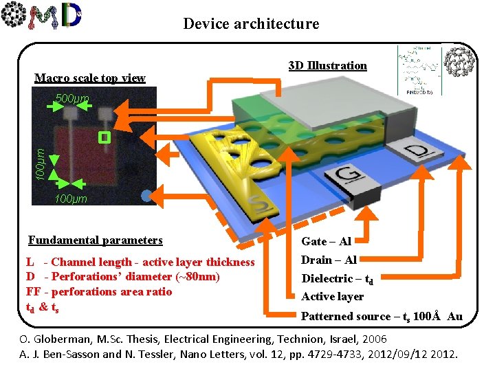
Device architecture Macro scale top view 3 D Illustration 100μm 500μm 100μm Fundamental parameters Gate – Al L - Channel length - active layer thickness D - Perforations’ diameter (~80 nm) FF - perforations area ratio td & t s Drain – Al Dielectric – td Active layer Patterned source – ts 100Å Au O. Globerman, M. Sc. Thesis, Electrical Engineering, Technion, Israel, 2006 A. J. Ben-Sasson and N. Tessler, Nano Letters, vol. 12, pp. 4729 -4733, 2012/09/12 2012.

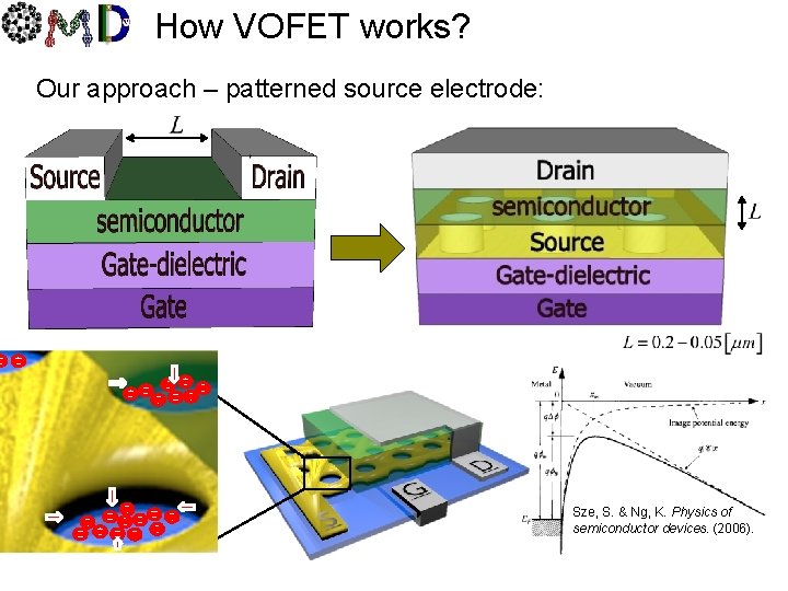
How VOFET works? Our approach – patterned source electrode: Sze, S. & Ng, K. Physics of semiconductor devices. (2006).

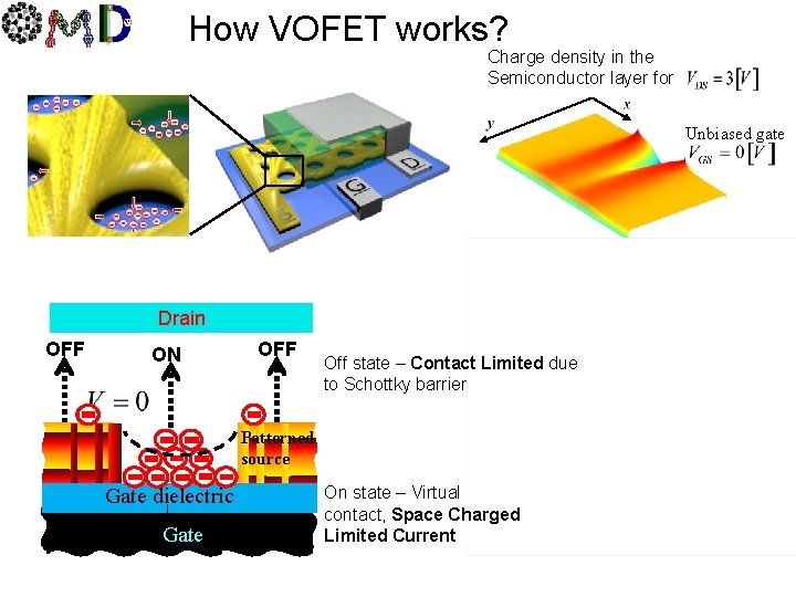
How VOFET works? Charge density in the Semiconductor layer for Unbiased gate Virtual contact Formation Drain OFF ON OFF Off state – Contact Limited due to Schottky barrier Patterned source Gate dielectric Gate On state – Virtual contact, Space Charged Limited Current Saturated virtual contact

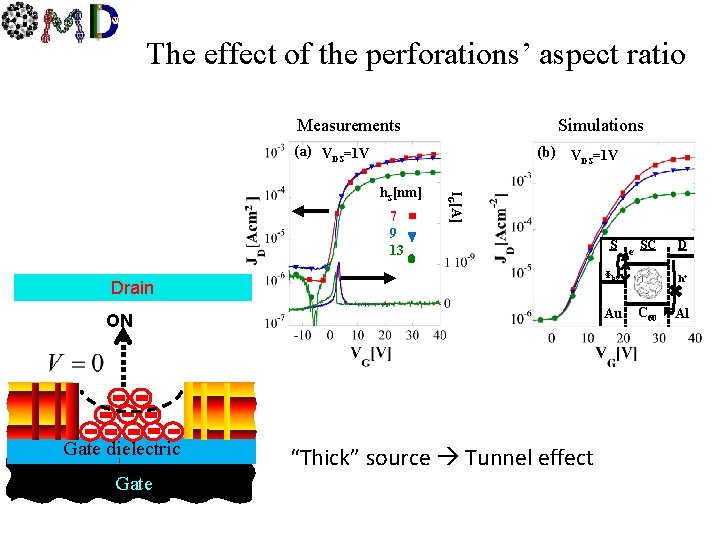
The effect of the perforations’ aspect ratio Measurements Simulations (a) VDS=1 V (b) VDS=1 V 7 9 13 IG[A] h. S[nm] Au ON Patterned source Gate e- SC Φb 0 Drain Gate dielectric S “Thick” source Tunnel effect D h+ C 60 Al

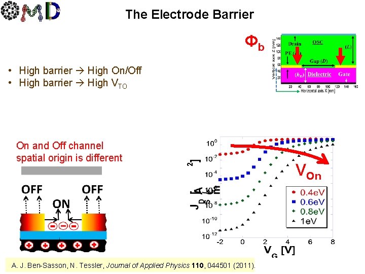
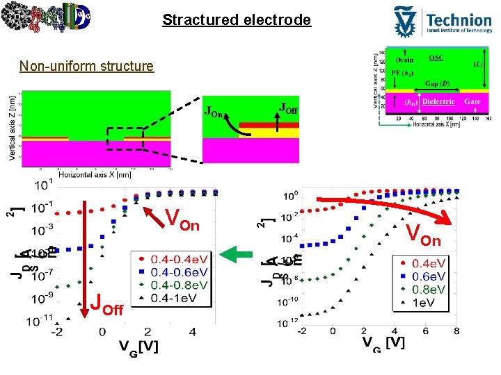
The Electrode Barrier Φb • High barrier High On/Off • High barrier High VTO On and Off channel spatial origin is different A. J. Ben-Sasson, N. Tessler, Journal of Applied Physics 110, 044501 (2011). VOn

V. B Stractured electrode Non-uniform structure JOn VOn JOff VOn

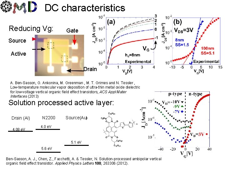
DC characteristics Reducing Vg: Gate Source Active Drain A. Ben-Sasson, G. Ankonina, M. Greenman , M. T. Grimes and N. Tessler , Low-temperature molecular vapor deposition of ultra-thin metal oxide dielectric for low-voltage vertical organic field effect transistors, ACS Appl Mater Interfaces (2013) Solution processed active layer: Drain (Al) 4. 08 e. V N 2200 Source(Au) 4. 0 e. V 5. 1 e. V 5. 6 e. V Ben-Sasson, A. J. , Chen, Z. , Facchetti, A. & Tessler, N. Solution-processed ambipolar vertical organic field effect transistor. Applied Physics Letters 100, 263306 (2012).

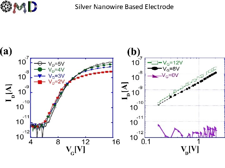
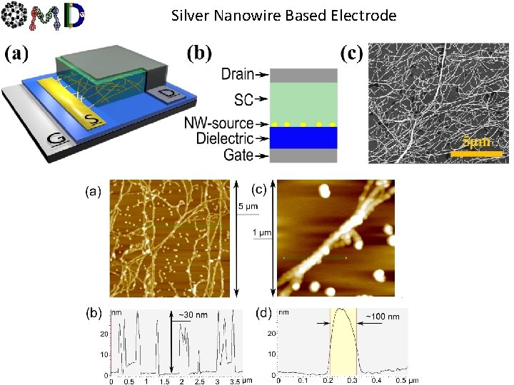
Silver Nanowire Based Electrode

Silver Nanowire Based Electrode

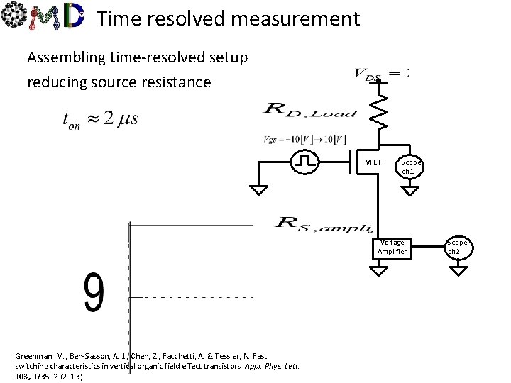
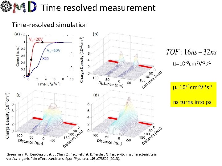
Time resolved measurement Assembling time-resolved setup reducing source resistance VFET Scope ch 1 Voltage Amplifier Greenman, M. , Ben-Sasson, A. J. , Chen, Z. , Facchetti, A. & Tessler, N. Fast switching characteristics in vertical organic field effect transistors. Appl. Phys. Lett. 103, 073502 (2013). Scope ch 2

Time resolved measurement Time-resolved simulation m=10 -3 cm 2 V-1 s-1 m=10+1 cm 2 V-1 s-1 ns turns into ps Greenman, M. , Ben-Sasson, A. J. , Chen, Z. , Facchetti, A. & Tessler, N. Fast switching characteristics in vertical organic field effect transistors. Appl. Phys. Lett. 103, 073502 (2013).

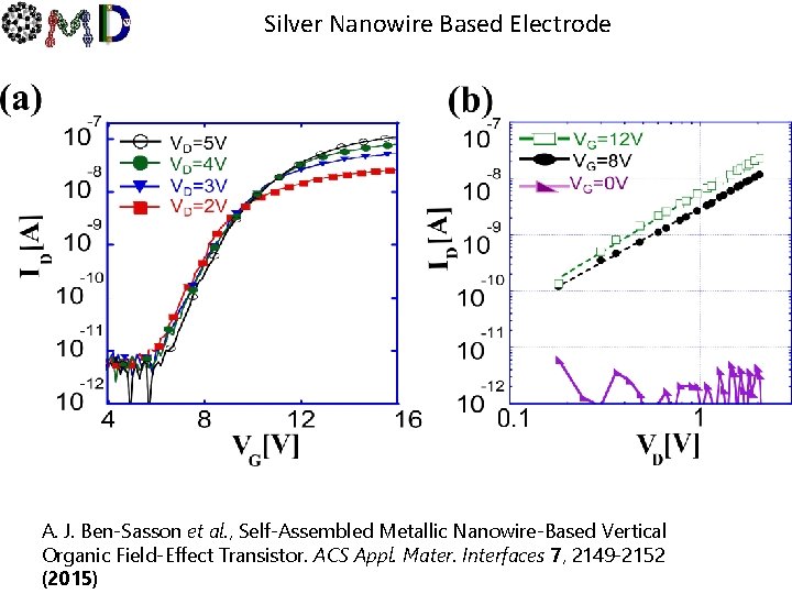
Silver Nanowire Based Electrode

Silver Nanowire Based Electrode A. J. Ben-Sasson et al. , Self-Assembled Metallic Nanowire-Based Vertical Organic Field-Effect Transistor. ACS Appl. Mater. Interfaces 7, 2149 -2152 (2015)

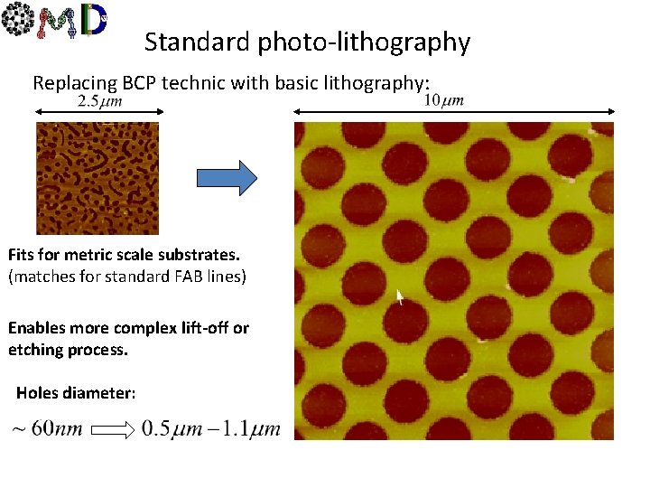
Standard photo-lithography Replacing BCP technic with basic lithography: Fits for metric scale substrates. (matches for standard FAB lines) Enables more complex lift-off or etching process. Holes diameter:

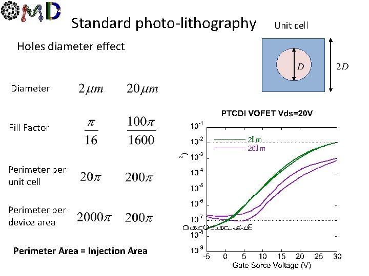
Standard photo-lithography Holes diameter effect Diameter Fill Factor Perimeter per unit cell Perimeter per device area Perimeter Area = Injection Area Unit cell

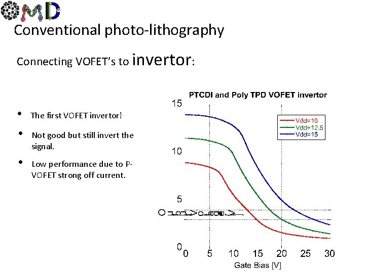
Conventional photo-lithography Connecting VOFET’s to invertor: • • The first VOFET invertor! • Low performance due to PVOFET strong off current. Not good but still invert the signal.

Thank You The fabrication was performed at the Micro. Nano Fabrication Unit (MNFU), Technion.