
Vertically scaled 5 nm Ga N channel Enhancementmode
- Slides: 20
Vertically scaled 5 nm Ga. N channel Enhancement-mode N-polar Ga. N MOS-HFET with 560 m. S/mm gm and 0. 76 W-mm Ron Uttam Singisetti*, Man Hoi Wong, Jim Speck, and Umesh Mishra ECE and Materials Departments University of California, Santa Barbara, CA 2011 Device Research Conference Santa Barbara, CA, USA *uttam@ece. ucsb. edu 1
Outline • Next generation Ga. N electronic devices • N-polar Ga. N HEMTs • Vertically scaled channel devices • Results and Conclusion 2
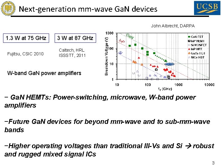
Next-generation mm-wave Ga. N devices John Albrecht, DARPA 1. 3 W at 75 GHz Fujitsu, CSIC 2010 3 W at 87 GHz Caltech, HRL ISSSTT, 2011 W-band Ga. N power amplifiers − Ga. N HEMTs: Power-switching, microwave, W-band power amplifiers −Future Ga. N devices for beyond mm-wave and to sub-mm-wave bands −Higher operating voltages than traditional III-Vs and Si robust and rugged mixed signal ICs 3
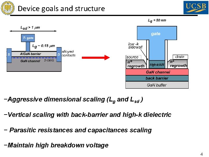
Device goals and structure −Aggressive dimensional scaling (Lg and Lsd ) −Vertical scaling with back-barrier and high-k dielectric − Parasitic resistances and capacitances scaling −Maintain high breakdown voltage 4
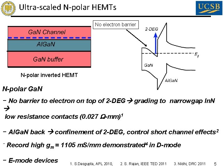
Ultra-scaled N-polar HEMTs No electron barrier N-polar inverted HEMT N-polar Ga. N − No barrier to electron on top of 2 -DEG grading to narrowgap In. N low resistance contacts (0. 027 W-mm)1 − Al. Ga. N back confinement of 2 -DEG, control short channel effects 2 − Record high gm = 1105 m. S/mm demonstrated 4 in D-mode − E-mode devices 1. S. Dasgupta, APL 2010, 2. S. Rajan, IEEE TED 2011 3. NIdhi, DRC 2011 5
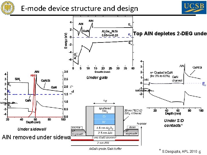
E-mode device structure and design Top Al. N depletes 2 -DEG under Under gate Under sidewall Under S/D contacts* Al. N removed under sidewall * S. Dasgupta, APL 2010 6
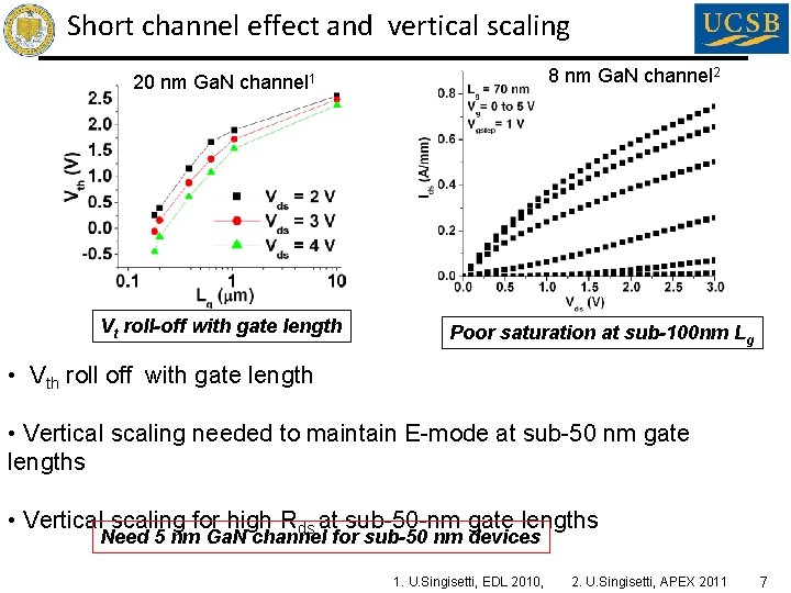
Short channel effect and vertical scaling 8 nm Ga. N channel 2 20 nm Ga. N channel 1 Vt roll-off with gate length Poor saturation at sub-100 nm Lg • Vth roll off with gate length • Vertical scaling needed to maintain E-mode at sub-50 nm gate lengths • Vertical scaling for high Rds at sub-50 -nm gate lengths Need 5 nm Ga. N channel for sub-50 nm devices 1. U. Singisetti, EDL 2010, 2. U. Singisetti, APEX 2011 7
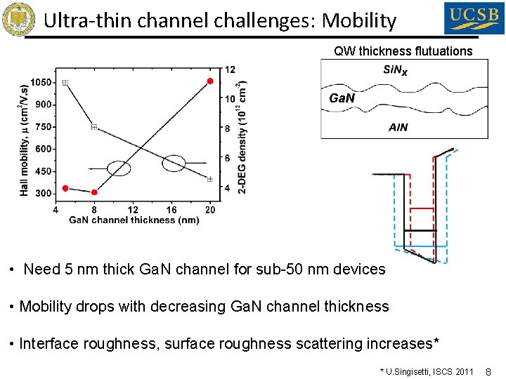
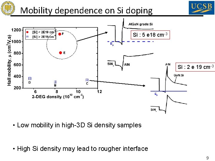
Ultra-thin channel challenges: Mobility QW thickness flutuations Ga. N • Need 5 nm thick Ga. N channel for sub-50 nm devices • Mobility drops with decreasing Ga. N channel thickness • Interface roughness, surface roughness scattering increases* * U. Singisetti, ISCS 2011 8
Mobility dependence on Si doping Si : 5 e 18 cm-3 Si : 2 e 19 cm-3 • Low mobility in high-3 D Si density samples • High Si density may lead to rougher interface 9
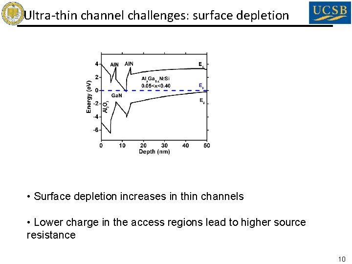
Ultra-thin channel challenges: surface depletion • Surface depletion increases in thin channels • Lower charge in the access regions lead to higher source resistance 10
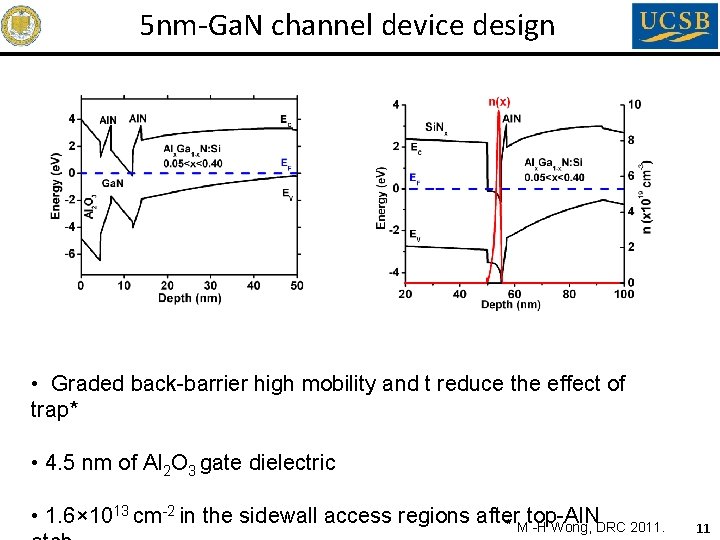
5 nm-Ga. N channel device design • Graded back-barrier high mobility and t reduce the effect of trap* • 4. 5 nm of Al 2 O 3 gate dielectric • 1. 6× 1013 cm-2 in the sidewall access regions after top-Al. N * M -H Wong, DRC 2011. 11
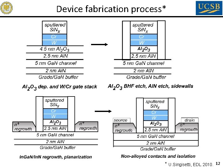
Device fabrication process* * U. Singisetti, EDL 2010. 12
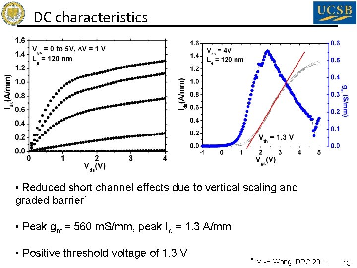
DC characteristics • Reduced short channel effects due to vertical scaling and graded barrier 1 • Peak gm = 560 m. S/mm, peak Id = 1. 3 A/mm • Positive threshold voltage of 1. 3 V * M -H Wong, DRC 2011. 13
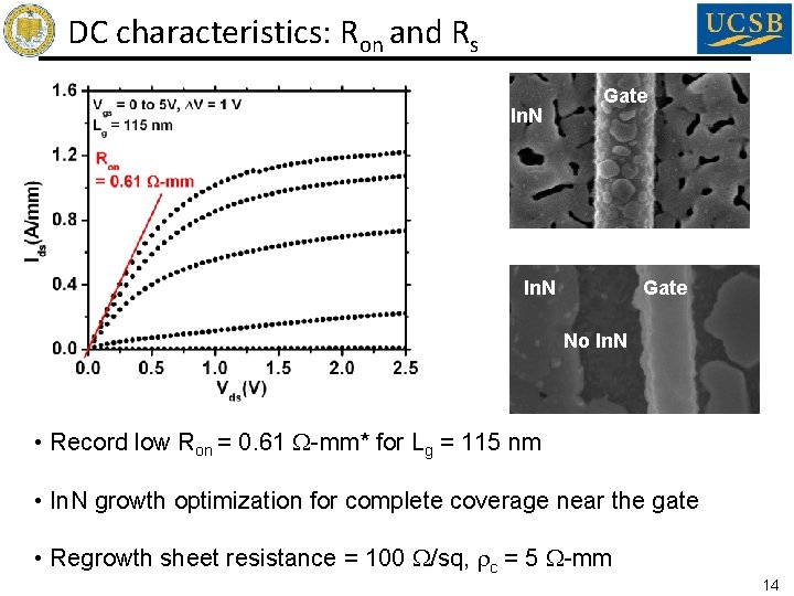
DC characteristics: Ron and Rs In. N Gate No In. N • Record low Ron = 0. 61 W-mm* for Lg = 115 nm • In. N growth optimization for complete coverage near the gate • Regrowth sheet resistance = 100 W/sq, rc = 5 W-mm 14
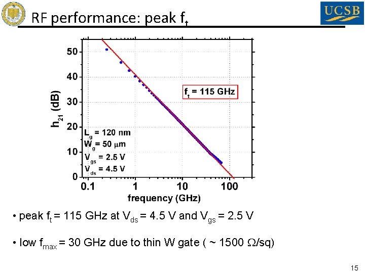
RF performance: peak ft • peak ft = 115 GHz at Vds = 4. 5 V and Vgs = 2. 5 V • low fmax = 30 GHz due to thin W gate ( ~ 1500 W/sq) 15
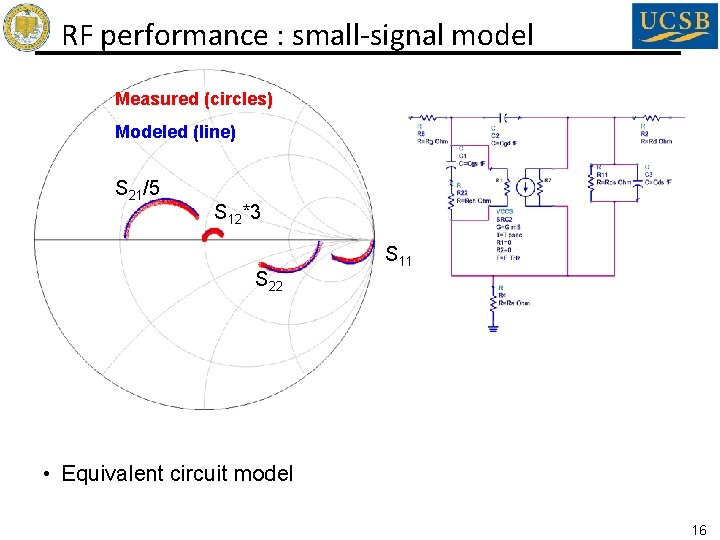
RF performance : small-signal model Measured (circles) Modeled (line) S 21/5 S 12*3 S 22 S 11 • Equivalent circuit model 16
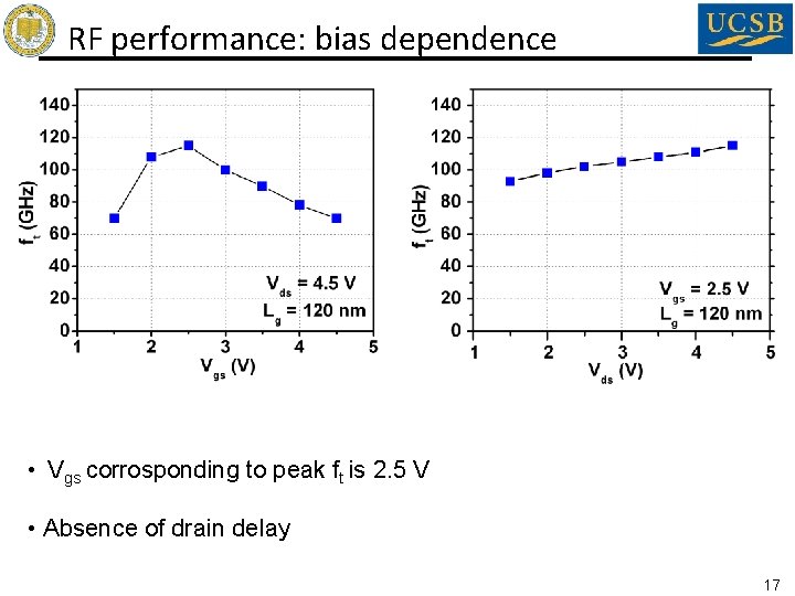
RF performance: bias dependence • Vgs corrosponding to peak ft is 2. 5 V • Absence of drain delay 17
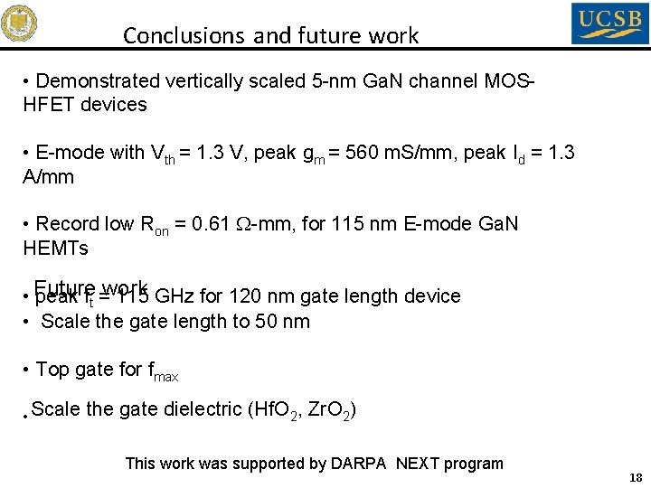
Conclusions and future work • Demonstrated vertically scaled 5 -nm Ga. N channel MOSHFET devices • E-mode with Vth = 1. 3 V, peak gm = 560 m. S/mm, peak Id = 1. 3 A/mm • Record low Ron = 0. 61 W-mm, for 115 nm E-mode Ga. N HEMTs • Future peak ft =work 115 GHz for 120 nm gate length device • Scale the gate length to 50 nm • Top gate for fmax • Scale the gate dielectric (Hf. O 2, Zr. O 2) This work was supported by DARPA NEXT program 18
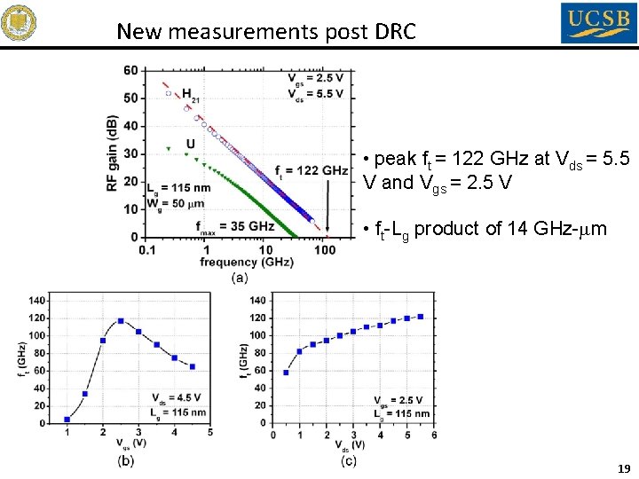
New measurements post DRC • peak ft = 122 GHz at Vds = 5. 5 V and Vgs = 2. 5 V • ft-Lg product of 14 GHz-mm 19
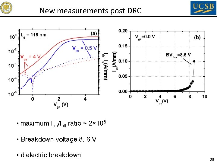
New measurements post DRC • maximum Ion/Ioff ratio ~ 2× 10⁵ • Breakdown voltage 8. 6 V • dielectric breakdown 20