Verilog HDL Introduction VLSI Group DAIICT Kishore Aditya


")


- Slides: 44
Verilog HDL -Introduction VLSI Group –DAIICT Kishore, Aditya & Harsha Ref: Verilog – HDL by samir palnitkar 2 nd Edition
Module- Basic building block A module can be an element or collection of low level design blocks
Levels of Abstraction-1 o Switch Level: Module implemented with switches and interconnects. Lowest level of Abstraction o Gate Level: Module implemented in terms of logic gates like (and , or) and interconnection between gates
Levels of Abstraction-2 o Dataflow Level: Module designed by specifying dataflow. The designer is aware of how data flows between hardware registers and how the data is processed in the design o Behavioral Level : Module can be implemented in terms of the desired design algorithm without concern for the hardware implementation details. Very similar to C programming
Hierrarchy
Basic Concepts o Number is specified as <size>'<baseformat><number>
Contd.
Nets o Nets represent connections between hardware elements. Just as in real circuits, nets have values continuously driven on them by the outputs of devices that they are connected to.
Registers o Registers represent data storage elements. Registers retain value until another value is placed onto them. o In Verilog, the term register merely means a variable that can hold a value. o Unlike a net, a register does not need a driver.
Vectors o Arrays of Regs and Nets
Integers and Parameters
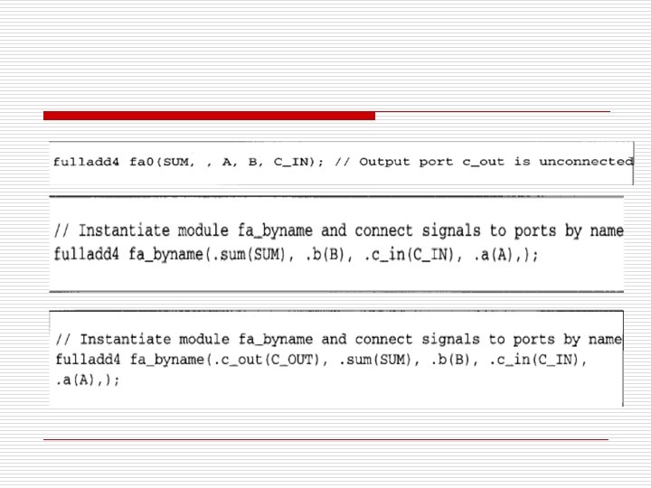
Ports o Ports provide interface for by which a module can communicate with its environment
Module
Port connection rules
Example
Connecting Ports o Suppose we have a module
Gate Level Modeling o A logic circuit can be designed by use of logic gates. o Verilog supports basic logic gates as predefined primitives. These primitives are instantiated like modules except that they are predefined in Verilog and do not need a module definition.
Gate gate_name(out, in 1, in 2…)
Buf/not gates o Buflnot gates have one scalar input and one or more scalar outputs.
Bufif/notif
Instantiation of bufif gates
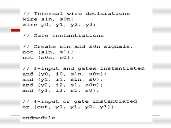
Design of 4: 1 Multiplexer
Contd. .
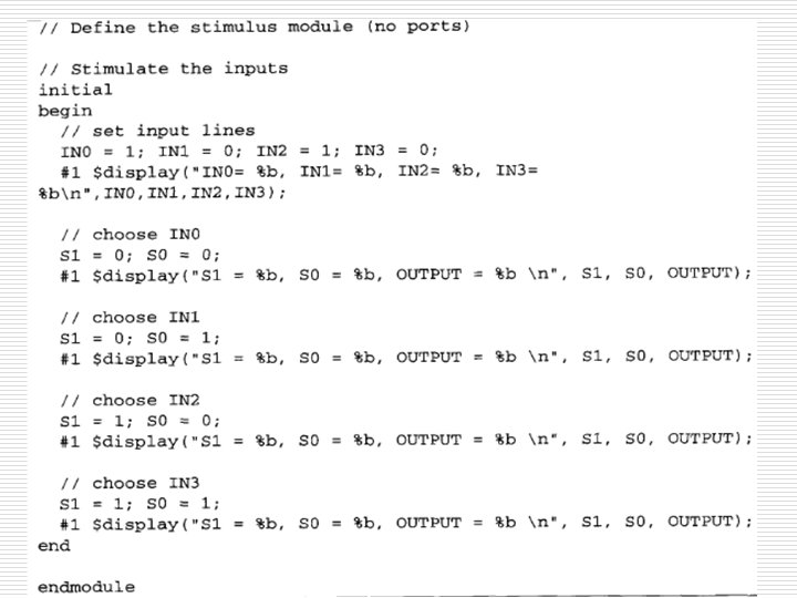
Stimulus
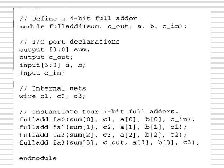
4 bit full adder
Declaration:
Code contd. .
4 bit adder using 1 bit adder
Stimulus
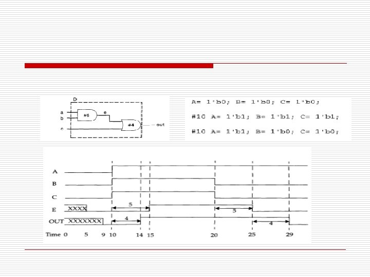
Gate Delays: o Rise Delay: Delay associated with a o/p transition to 1 from any value. Fall Delay: Delay associated with o/p transition to 0 from any value. Turn off Delay: Delay associate with o/p transition to Z from another value.
Dataflow Modeling o In complex designs the number of gates is very large o Currently, automated tools are used to create a gate-level circuit from a dataflow design description. This process is called logic synthesis
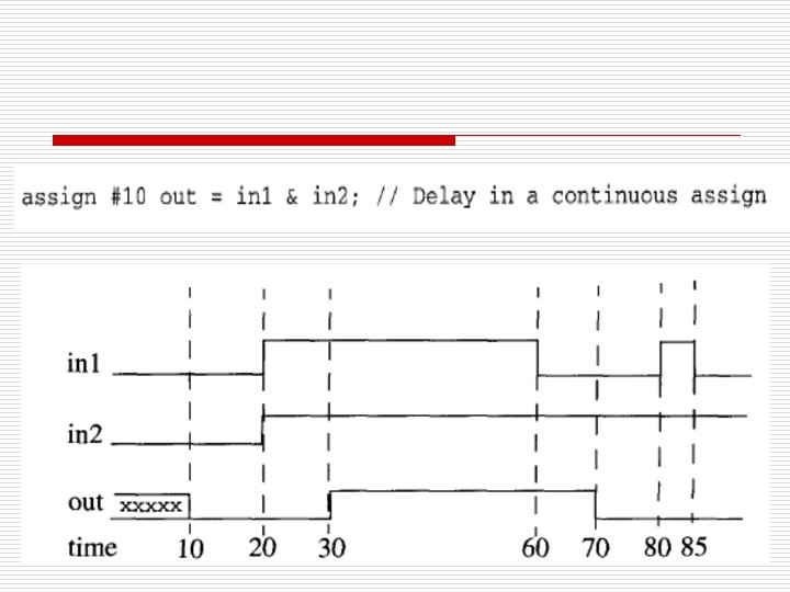
Continuous Assignment
Rules: o The left hand side of an assignment must always be a scalar or vector net o It cannot be a scalar or vector register. o Continuous assignments are always active. o The assignment expression is evaluated as soon as one of the right-hand-side operands changes and the value is assigned to the left-hand-side net.
o The operands on the right-hand side can be registers or nets. o Delay values can be specified for assignments in terms of time units. Delay values are used to control the time when a net is assigned the evaluated value
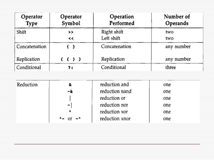
Operator Types
Conditional Operator
4: 1 Multiplexer Example