Verilog FPGA Digital Design Standard HDL languages Standards

![Verilog: module (2001) „module” name „module” keyword module test( input clk, input [7: 0] Verilog: module (2001) „module” name „module” keyword module test( input clk, input [7: 0]](https://slidetodoc.com/presentation_image/248aef338f6368e64b32e59b750bf3fa/image-8.jpg)
![Example – 4 bit adder, structural module add 4 (input [3: 0] a, b, Example – 4 bit adder, structural module add 4 (input [3: 0] a, b,](https://slidetodoc.com/presentation_image/248aef338f6368e64b32e59b750bf3fa/image-32.jpg)
![FSM example – Verilog (1) module light( input clk, rst, output reg [2: 0] FSM example – Verilog (1) module light( input clk, rst, output reg [2: 0]](https://slidetodoc.com/presentation_image/248aef338f6368e64b32e59b750bf3fa/image-41.jpg)
![File operations • Reading data into an array reg [9: 0] input_data[255: 0]; initial File operations • Reading data into an array reg [9: 0] input_data[255: 0]; initial](https://slidetodoc.com/presentation_image/248aef338f6368e64b32e59b750bf3fa/image-51.jpg)
![LUT ROM • ROM (asynchronous) – HDL code module rom 16 (input [3: 0] LUT ROM • ROM (asynchronous) – HDL code module rom 16 (input [3: 0]](https://slidetodoc.com/presentation_image/248aef338f6368e64b32e59b750bf3fa/image-61.jpg)
![Shift register array module shr_16 x 8 (input clk, sh, input [3: 0] addr, Shift register array module shr_16 x 8 (input clk, sh, input [3: 0] addr,](https://slidetodoc.com/presentation_image/248aef338f6368e64b32e59b750bf3fa/image-65.jpg)

![DP Block. RAM module dp_ram(input clk_a, we_a, en_a, clk_b, we_b, en_b, input [10: 0] DP Block. RAM module dp_ram(input clk_a, we_a, en_a, clk_b, we_b, en_b, input [10: 0]](https://slidetodoc.com/presentation_image/248aef338f6368e64b32e59b750bf3fa/image-73.jpg)
- Slides: 74

Verilog & FPGA Digital Design

Standard HDL languages • Standards HDL (hardware description language) languages – Verilog • 1984: Gateway Design Automation Inc. • 1990: Cadence -> Open Verilog International • 1995: IEEE standardization • 2001: Verilog 2001 – VHDL • 1983 -85: IBM, Texas Instruments • 1987: IEEE standardization • 1994: VHDL-1993

Other HDL languages • HDL development is very time consuming compared to software development • Lot of programmers with C/C++ knowledge, much less HDL designer • High level hardware description languages – Celoxica Handel-C: based on ANSI-C with special features – System. C: standardized, object oriented C++ based language – Mentor Catapult-C: can generate hardware from standard C code • Faster simulation, verification • HW/SW co-design

Purpose of HDL languages • Modeling hardware behavior – Large part of these languages can only be used for simulation, not for hardware generation (synthesis) – Synthesizable part depends on the actual synthesizer • Replace graphical, schematic based design method (which very time consuming) • RTL (Register Transfer Level) level description – Automatic hardware synthesis – Increase productivity

HDL languages • Modular languages • HDL module – Input and output port definitions – Logic equations between the inputs and the outputs • Unlike software programming languages, NOT a sequential language – Describes PARALLEL OPERATIONS

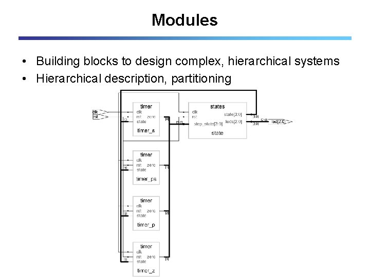
Modules • Building blocks to design complex, hierarchical systems • Hierarchical description, partitioning

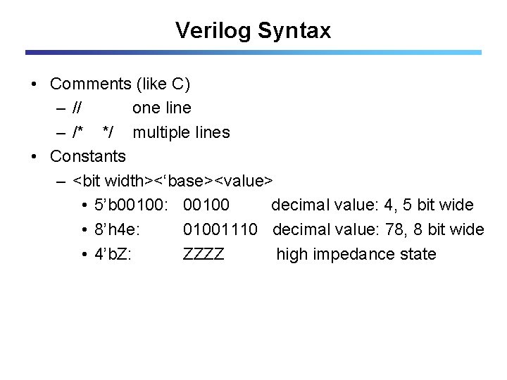
Verilog Syntax • Comments (like C) – // one line – /* */ multiple lines • Constants – <bit width><‘base><value> • 5’b 00100: 00100 decimal value: 4, 5 bit wide • 8’h 4 e: 01001110 decimal value: 78, 8 bit wide • 4’b. Z: ZZZZ high impedance state
![Verilog module 2001 module name module keyword module test input clk input 7 0 Verilog: module (2001) „module” name „module” keyword module test( input clk, input [7: 0]](https://slidetodoc.com/presentation_image/248aef338f6368e64b32e59b750bf3fa/image-8.jpg)
Verilog: module (2001) „module” name „module” keyword module test( input clk, input [7: 0] data_in, output [7: 0] data_out, output reg valid ); ……. ……. endmodule „endmodule” keyword Input ports Output ports Functional description

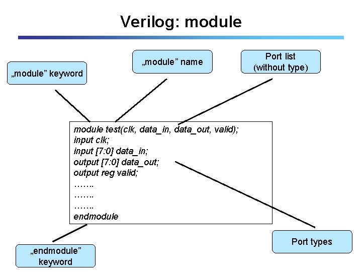
Verilog: module „module” name „module” keyword Port list (without type) module test(clk, data_in, data_out, valid); input clk; input [7: 0] data_in; output [7: 0] data_out; output reg valid; ……. ……. endmodule „endmodule” keyword Port types

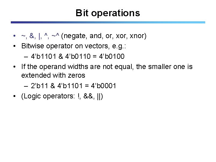
Bit operations • ~, &, |, ^, ~^ (negate, and, or, xnor) • Bitwise operator on vectors, e. g. : – 4’b 1101 & 4’b 0110 = 4’b 0100 • If the operand widths are not equal, the smaller one is extended with zeros – 2’b 11 & 4’b 1101 = 4’b 0001 • (Logic operators: !, &&, ||)

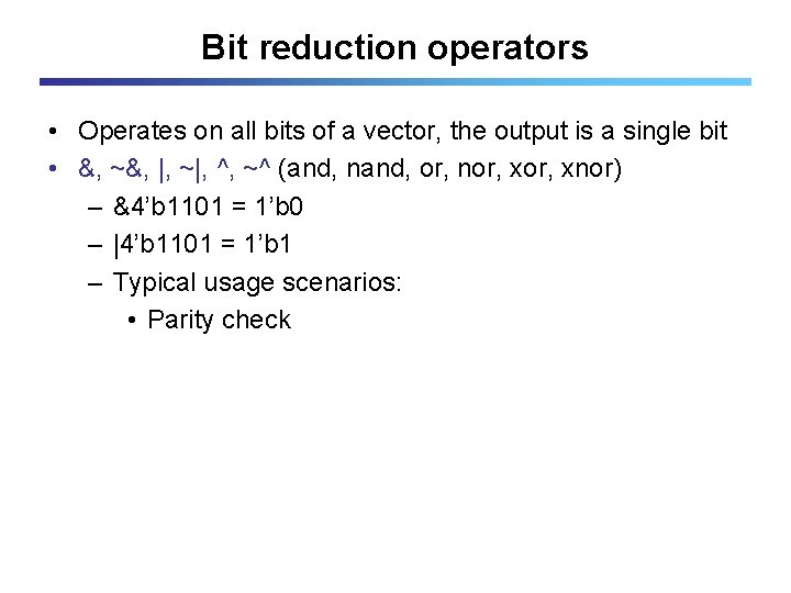
Bit reduction operators • Operates on all bits of a vector, the output is a single bit • &, ~&, |, ~|, ^, ~^ (and, nand, or, nor, xnor) – &4’b 1101 = 1’b 0 – |4’b 1101 = 1’b 1 – Typical usage scenarios: • Parity check

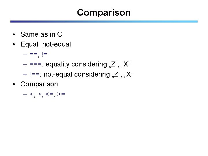
Comparison • Same as in C • Equal, not-equal – ==, != – ===: equality considering „Z”, „X” – !==: not-equal considering „Z”, „X” • Comparison – <, >, <=, >=

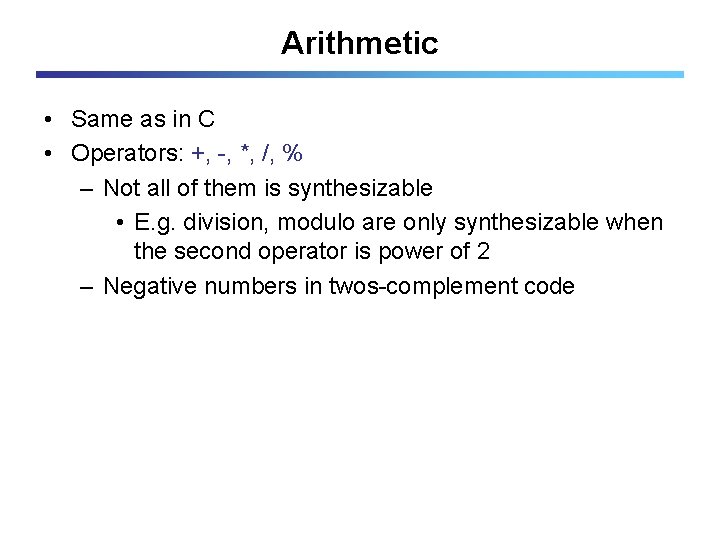
Arithmetic • Same as in C • Operators: +, -, *, /, % – Not all of them is synthesizable • E. g. division, modulo are only synthesizable when the second operator is power of 2 – Negative numbers in twos-complement code

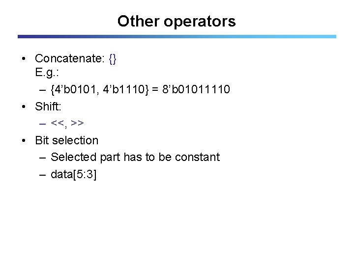
Other operators • Concatenate: {} E. g. : – {4’b 0101, 4’b 1110} = 8’b 01011110 • Shift: – <<, >> • Bit selection – Selected part has to be constant – data[5: 3]

Data types • wire – Behaves like a real wire (combinatorial logic) – Declaration of an 8 bit wire: wire [7: 0] data; • reg – After synthesis it can translate into • Wire • Latch • Flip-flop – E. g. : reg [7: 0] data;

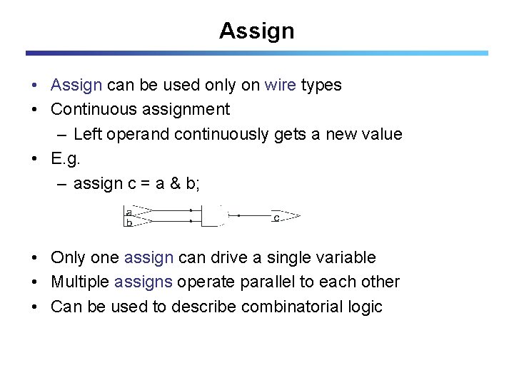
Assign • Assign can be used only on wire types • Continuous assignment – Left operand continuously gets a new value • E. g. – assign c = a & b; • Only one assign can drive a single variable • Multiple assigns operate parallel to each other • Can be used to describe combinatorial logic

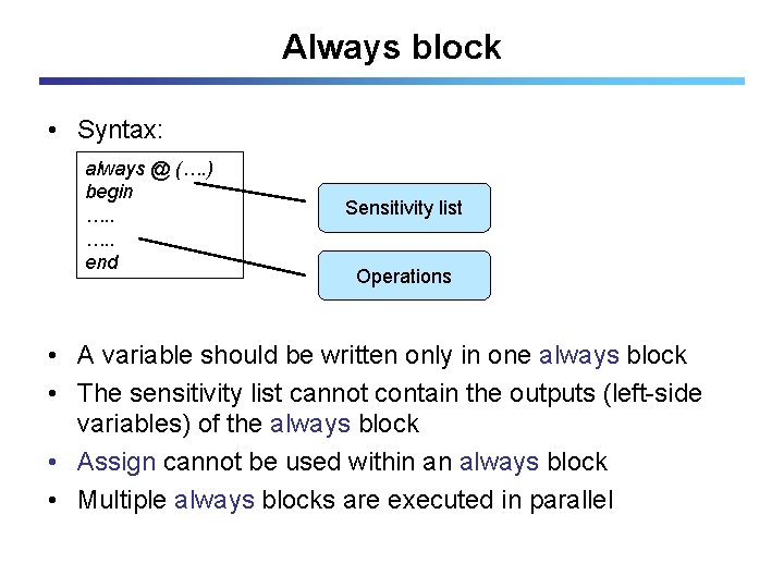
Always block • Syntax: always @ (…. ) begin …. . end Sensitivity list Operations • A variable should be written only in one always block • The sensitivity list cannot contain the outputs (left-side variables) of the always block • Assign cannot be used within an always block • Multiple always blocks are executed in parallel

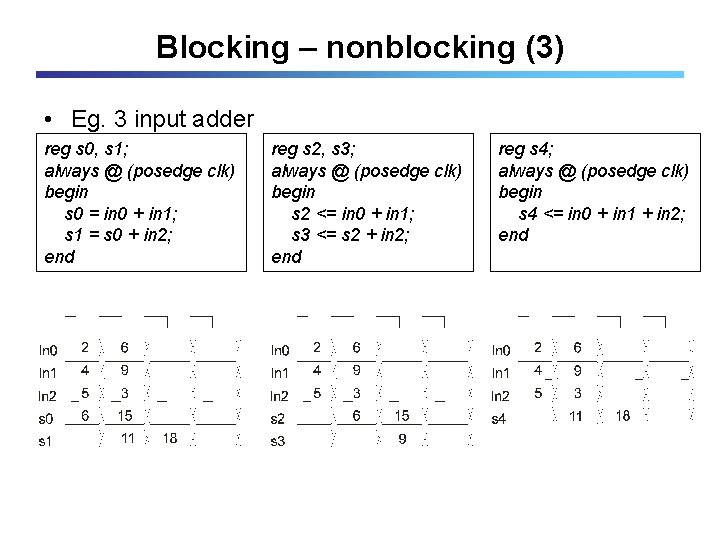
Always – assignments • Blocking: = – Blocks the execution of operations after it till it is executed -> sequential operation (don’t use it unless really necessary) • Nonblocking: <= – Nonblocking assignments are executed in parallel -> hardware-like operation • Always use nonblocking assignment

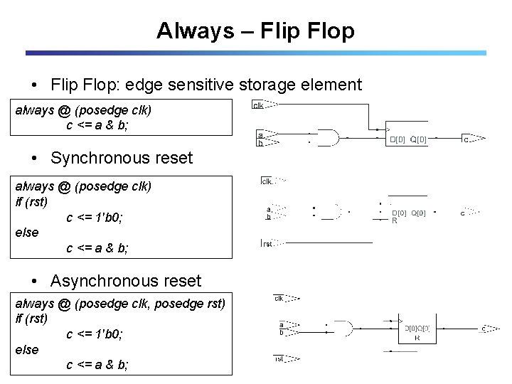
Always – Flip Flop • Flip Flop: edge sensitive storage element always @ (posedge clk) c <= a & b; • Synchronous reset always @ (posedge clk) if (rst) c <= 1'b 0; else c <= a & b; • Asynchronous reset always @ (posedge clk, posedge rst) if (rst) c <= 1'b 0; else c <= a & b;

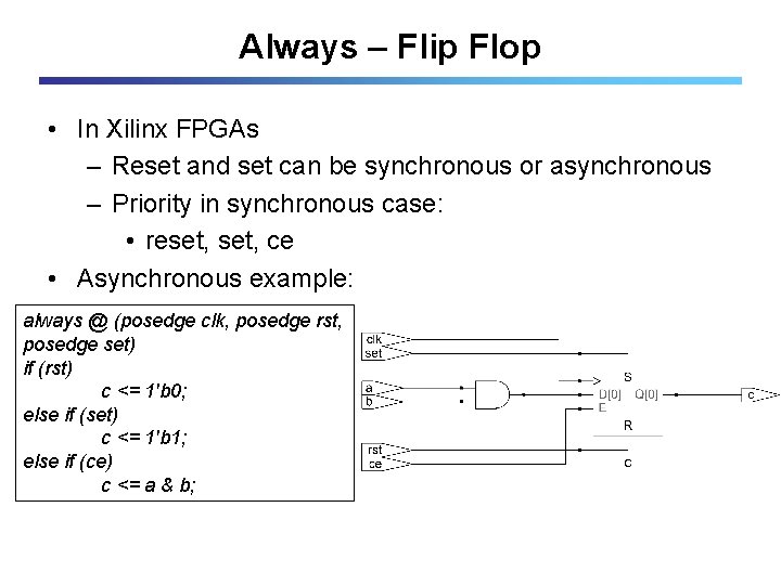
Always – Flip Flop • In Xilinx FPGAs – Reset and set can be synchronous or asynchronous – Priority in synchronous case: • reset, ce • Asynchronous example: always @ (posedge clk, posedge rst, posedge set) if (rst) c <= 1'b 0; else if (set) c <= 1'b 1; else if (ce) c <= a & b;

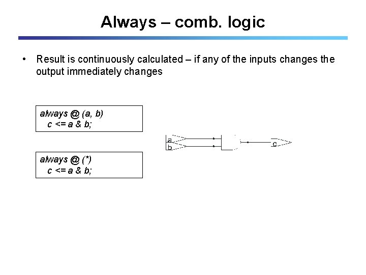
Always – comb. logic • Result is continuously calculated – if any of the inputs changes the output immediately changes always @ (a, b) c <= a & b; always @ (*) c <= a & b;

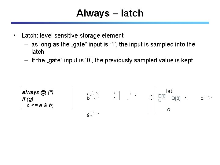
Always – latch • Latch: level sensitive storage element – as long as the „gate” input is ‘ 1’, the input is sampled into the latch – If the „gate” input is ‘ 0’, the previously sampled value is kept always @ (*) If (g) c <= a & b;

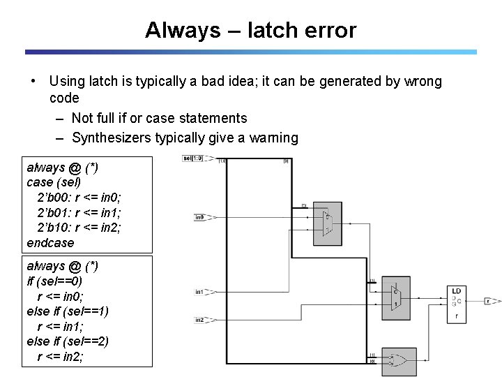
Always – latch error • Using latch is typically a bad idea; it can be generated by wrong code – Not full if or case statements – Synthesizers typically give a warning always @ (*) case (sel) 2’b 00: r <= in 0; 2’b 01: r <= in 1; 2’b 10: r <= in 2; endcase always @ (*) if (sel==0) r <= in 0; else if (sel==1) r <= in 1; else if (sel==2) r <= in 2;

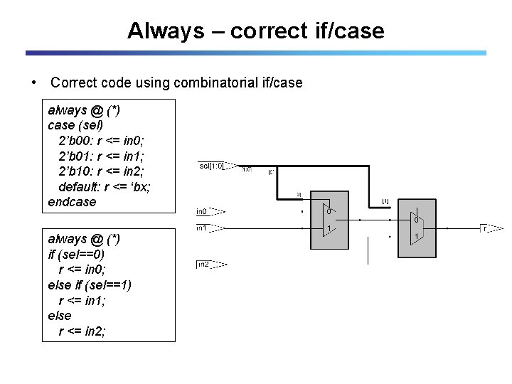
Always – correct if/case • Correct code using combinatorial if/case always @ (*) case (sel) 2’b 00: r <= in 0; 2’b 01: r <= in 1; 2’b 10: r <= in 2; default: r <= ‘bx; endcase always @ (*) if (sel==0) r <= in 0; else if (sel==1) r <= in 1; else r <= in 2;

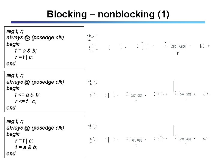
Blocking – nonblocking (1) reg t, r; always @ (posedge clk) begin t = a & b; r = t | c; end reg t, r; always @ (posedge clk) begin t <= a & b; r <= t | c; end reg t, r; always @ (posedge clk) begin r = t | c; t = a & b; end

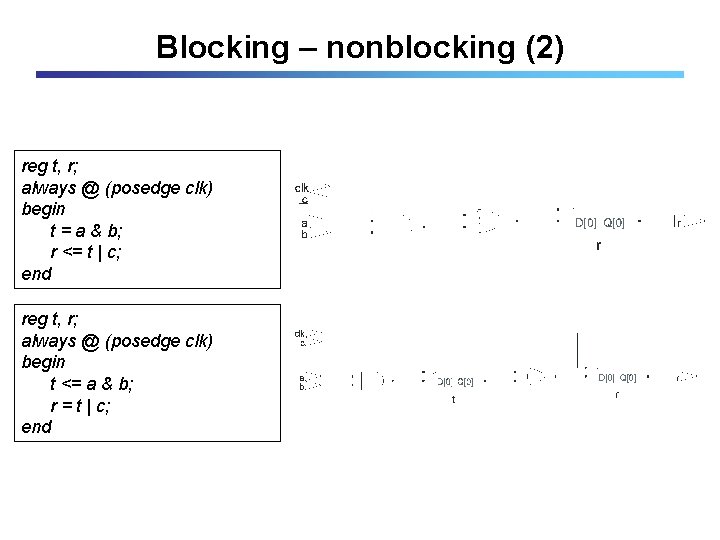
Blocking – nonblocking (2) reg t, r; always @ (posedge clk) begin t = a & b; r <= t | c; end reg t, r; always @ (posedge clk) begin t <= a & b; r = t | c; end

Blocking – nonblocking (3) • Eg. 3 input adder reg s 0, s 1; always @ (posedge clk) begin s 0 = in 0 + in 1; s 1 = s 0 + in 2; end reg s 2, s 3; always @ (posedge clk) begin s 2 <= in 0 + in 1; s 3 <= s 2 + in 2; end reg s 4; always @ (posedge clk) begin s 4 <= in 0 + in 1 + in 2; end

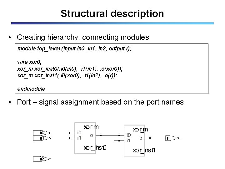
Structural description • Creating hierarchy: connecting modules module top_level (input in 0, in 1, in 2, output r); wire xor 0; xor_m xor_inst 0(. i 0(in 0), . i 1(in 1), . o(xor 0)); xor_m xor_inst 1(. i 0(xor 0), . i 1(in 2), . o(r)); endmodule • Port – signal assignment based on the port names

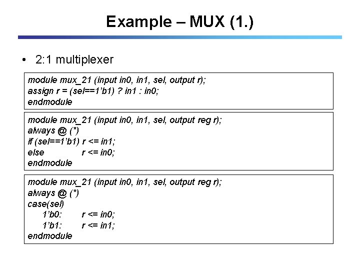
Example – MUX (1. ) • 2: 1 multiplexer module mux_21 (input in 0, in 1, sel, output r); assign r = (sel==1’b 1) ? in 1 : in 0; endmodule mux_21 (input in 0, in 1, sel, output reg r); always @ (*) if (sel==1’b 1) r <= in 1; else r <= in 0; endmodule mux_21 (input in 0, in 1, sel, output reg r); always @ (*) case(sel) 1’b 0: r <= in 0; 1’b 1: r <= in 1; endmodule

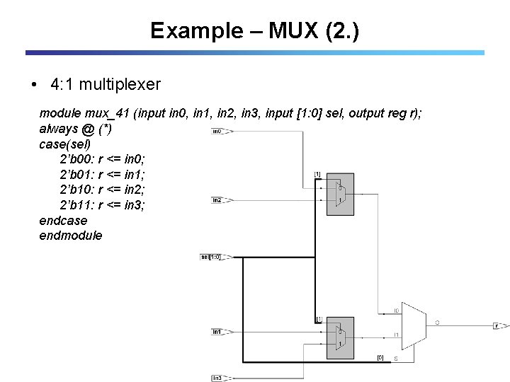
Example – MUX (2. ) • 4: 1 multiplexer module mux_41 (input in 0, in 1, in 2, in 3, input [1: 0] sel, output reg r); always @ (*) case(sel) 2’b 00: r <= in 0; 2’b 01: r <= in 1; 2’b 10: r <= in 2; 2’b 11: r <= in 3; endcase endmodule

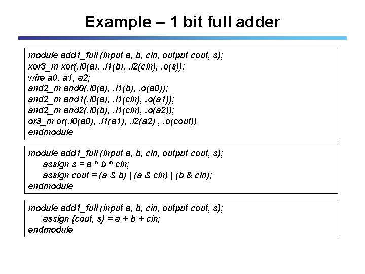
Example – 1 bit full adder module add 1_full (input a, b, cin, output cout, s); xor 3_m xor(. i 0(a), . i 1(b), . i 2(cin), . o(s)); wire a 0, a 1, a 2; and 2_m and 0(. i 0(a), . i 1(b), . o(a 0)); and 2_m and 1(. i 0(a), . i 1(cin), . o(a 1)); and 2_m and 2(. i 0(b), . i 1(cin), . o(a 2)); or 3_m or(. i 0(a 0), . i 1(a 1), . i 2(a 2) , . o(cout)) endmodule add 1_full (input a, b, cin, output cout, s); assign s = a ^ b ^ cin; assign cout = (a & b) | (a & cin) | (b & cin); endmodule add 1_full (input a, b, cin, output cout, s); assign {cout, s} = a + b + cin; endmodule
![Example 4 bit adder structural module add 4 input 3 0 a b Example – 4 bit adder, structural module add 4 (input [3: 0] a, b,](https://slidetodoc.com/presentation_image/248aef338f6368e64b32e59b750bf3fa/image-32.jpg)
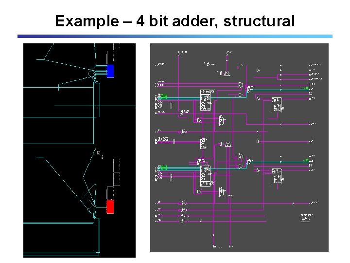
Example – 4 bit adder, structural module add 4 (input [3: 0] a, b, output [4: 0] s); wire [3: 0] cout; add 1_full add 0(. a(a[0]), . b(b[0]), . cin(1'b 0), . cout(cout[0]), . s(s[0])); add 1_full add 1(. a(a[1]), . b(b[1]), . cin(cout[0]), . cout(cout[1]), . s(s[1])); add 1_full add 2(. a(a[2]), . b(b[2]), . cin(cout[1]), . cout(cout[2]), . s(s[2])); add 1_full add 3(. a(a[3]), . b(b[3]), . cin(cout[2]), . cout(s[4]), . s(s[3])); endmodule add 4 (input [3: 0] a, b, input cin, output cout, output [3: 0] sum); assign {cout, sum} = a + b + cin; endmodule

Example – 4 bit adder, structural

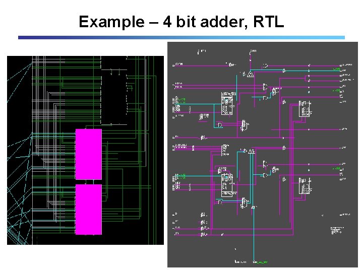
Example – 4 bit adder, RTL

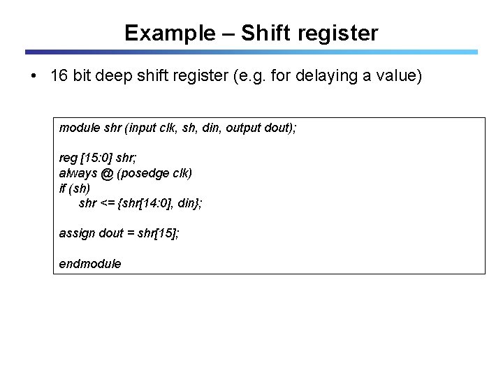
Example – Shift register • 16 bit deep shift register (e. g. for delaying a value) module shr (input clk, sh, din, output dout); reg [15: 0] shr; always @ (posedge clk) if (sh) shr <= {shr[14: 0], din}; assign dout = shr[15]; endmodule

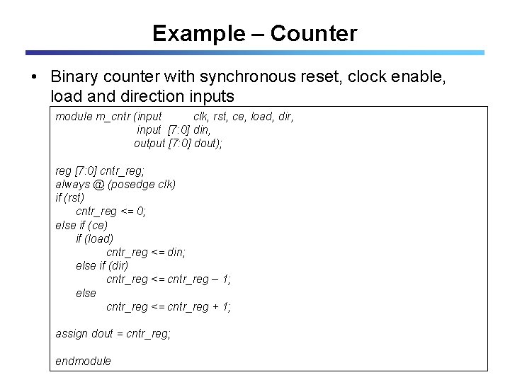
Example – Counter • Binary counter with synchronous reset, clock enable, load and direction inputs module m_cntr (input clk, rst, ce, load, dir, input [7: 0] din, output [7: 0] dout); reg [7: 0] cntr_reg; always @ (posedge clk) if (rst) cntr_reg <= 0; else if (ce) if (load) cntr_reg <= din; else if (dir) cntr_reg <= cntr_reg – 1; else cntr_reg <= cntr_reg + 1; assign dout = cntr_reg; endmodule

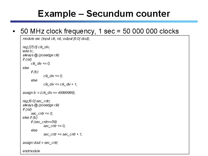
Example – Secundum counter • 50 MHz clock frequency, 1 sec = 50 000 clocks module sec (input clk, rst, output [6: 0] dout); reg [25: 0] clk_div; wire tc; always @ (posedge clk) If (rst) clk_div <= 0; else if (tc) clk_div <= 0; else clk_div <= clk_div + 1; assign tc = (clk_div == 49999999); reg [6: 0] sec_cntr; always @ (posedge clk) If (rst) sec_cntr <= 0; else if (tc) if (sec_cntr==59) sec_cntr <= 0; else sec_cntr <= sec_cntr + 1; assign dout = sec_cntr; endmodule

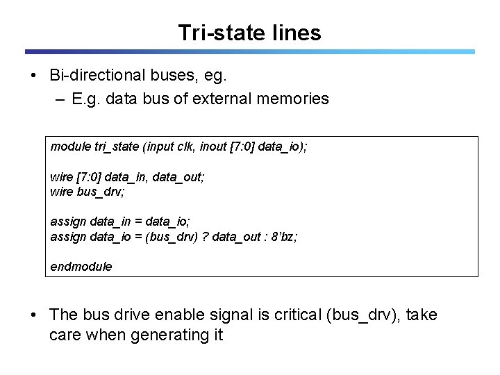
Tri-state lines • Bi-directional buses, eg. – E. g. data bus of external memories module tri_state (input clk, inout [7: 0] data_io); wire [7: 0] data_in, data_out; wire bus_drv; assign data_in = data_io; assign data_io = (bus_drv) ? data_out : 8’bz; endmodule • The bus drive enable signal is critical (bus_drv), take care when generating it

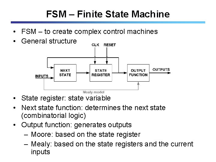
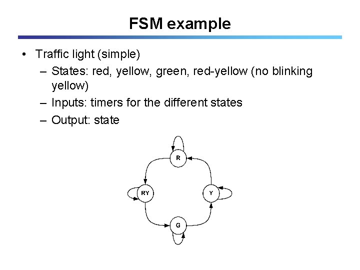
FSM – Finite State Machine • FSM – to create complex control machines • General structure • State register: state variable • Next state function: determines the next state (combinatorial logic) • Output function: generates outputs – Moore: based on the state register – Mealy: based on the state registers and the current inputs

FSM example • Traffic light (simple) – States: red, yellow, green, red-yellow (no blinking yellow) – Inputs: timers for the different states – Output: state
![FSM example Verilog 1 module light input clk rst output reg 2 0 FSM example – Verilog (1) module light( input clk, rst, output reg [2: 0]](https://slidetodoc.com/presentation_image/248aef338f6368e64b32e59b750bf3fa/image-41.jpg)
FSM example – Verilog (1) module light( input clk, rst, output reg [2: 0] led); parameter RED parameter RY parameter GREEN parameter YELLOW = 2'b 00; = 2'b 01; = 2'b 10; = 2'b 11; reg [15: 0] timer; reg [1: 0] state_reg; reg [1: 0] next_state; always @ (posedge clk) if (rst) state_reg <= RED; else state_reg <= next_state; always @ (*) case(state_reg) RED: begin if (timer == 0) next_state <= RY; else next_state <= R; end RY: begin if (timer == 0) next_state <= GREEN; else next_state <= RY; end YELLOW: begin if (timer == 0) next_state <= RED; else next_state <= YELLOW; end GREEN: begin if (timer == 0) next_state <= YELLOW; else next_state <= GREEN; end default: next_state <= 3'bxxx; endcase

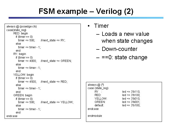
FSM example – Verilog (2) always @ (posedge clk) case(state_reg) RED: begin if (timer == 0) timer <= 500; //next_state <= RY; else timer <= timer - 1; end RY: begin if (timer == 0) timer <= 4000; //next_state <= GREEN; else timer <= timer - 1; end YELLOW: begin if (timer == 0) timer <= 4500; //next_state <= RED; else timer <= timer - 1; end GREEN: begin if (timer == 0) timer <= 500; //next_state <= YELLOW; else timer <= timer - 1; endcase • Timer – Loads a new value when state changes – Down-counter – ==0: state change always @ (*) case (state_reg) RY : RED: YELLOW: GREEN: default: endcase endmodule led <= 3'b 110; led <= 3'b 100; led <= 3'b 010; led <= 3'b 001; led <= 3’b 100;

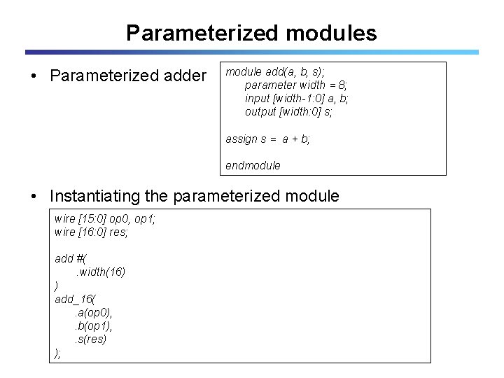
Parameterized modules • Parameterized adder module add(a, b, s); parameter width = 8; input [width-1: 0] a, b; output [width: 0] s; assign s = a + b; endmodule • Instantiating the parameterized module wire [15: 0] op 0, op 1; wire [16: 0] res; add #(. width(16) ) add_16(. a(op 0), . b(op 1), . s(res) );

Simulation • Testbench creation: two possibilities in Xilinx ISE – Testbench Waveform • Generating inputs using a GUI – Verilog Test Fixture • Generating inputs using Verilog • Simulator – ISE Simulator – Modelsim (MXE)

Verilog Test Fixture • Test Fixture – Test Fixture is a Verilog module – The module under test is a sub-module of the test fixture – All Verilog syntax constructs can be used – There are non-synthesizable constructs • Time base – ‘timescale 1 ns/1 ps • Time base is 1 ns • Simulation resolution: 1 ps

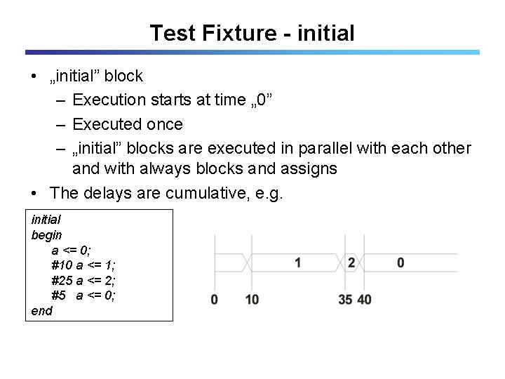
Test Fixture - initial • „initial” block – Execution starts at time „ 0” – Executed once – „initial” blocks are executed in parallel with each other and with always blocks and assigns • The delays are cumulative, e. g. initial begin a <= 0; #10 a <= 1; #25 a <= 2; #5 a <= 0; end

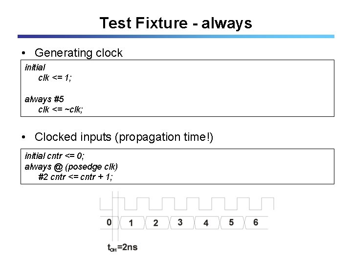
Test Fixture - always • Generating clock initial clk <= 1; always #5 clk <= ~clk; • Clocked inputs (propagation time!) initial cntr <= 0; always @ (posedge clk) #2 cntr <= cntr + 1;

Task • Declaration: – In the module which uses the task – In a different file (more modules can use the same task) • Arbitrary number of inputs and outputs • Can contain timing • Variables declared in a task are local variables • Global variables can be read or written by the task • A task can call another task

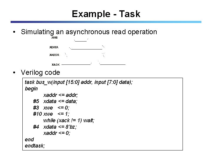
Example - Task • Simulating an asynchronous read operation • Verilog code task bus_w(input [15: 0] addr, input [7: 0] data); begin xaddr <= addr; #5 xdata <= data; #3 xwe <= 0; #10 xwe <= 1; while (xack != 1) wait; #4 xdata <= 8’bz; xaddr <= 0; endtask;

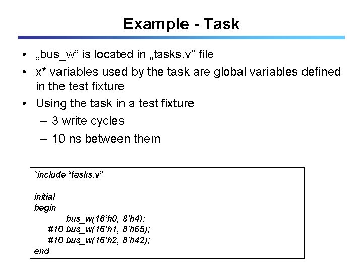
Example - Task • „bus_w” is located in „tasks. v” file • x* variables used by the task are global variables defined in the test fixture • Using the task in a test fixture – 3 write cycles – 10 ns between them `include “tasks. v” initial begin bus_w(16’h 0, 8’h 4); #10 bus_w(16’h 1, 8’h 65); #10 bus_w(16’h 2, 8’h 42); end
![File operations Reading data into an array reg 9 0 inputdata255 0 initial File operations • Reading data into an array reg [9: 0] input_data[255: 0]; initial](https://slidetodoc.com/presentation_image/248aef338f6368e64b32e59b750bf3fa/image-51.jpg)
File operations • Reading data into an array reg [9: 0] input_data[255: 0]; initial $readmemh(“input. txt”, input_data); • Writing data into a file integer file_out; wire res_valid; wire [16: 0] res; initial file_out =$fopen(“output. txt"); always @ (posedge clk) if (out_valid) $fwrite(file_out, "%d n", res);

FPGAs • FPGA: Field Programmable Gate Array – Programmable logic devices • Manufacturers: Xilinx, Altera, Actel, Quicklogic, Lattice • Features – Function is defined by the configuration – Configuration can be modified, changed – Complexity • 50000 – 8000000 system gates • 100 – 600 I/O pins • 100 – 400 MHz operating frequency (design dependant) – Architecture: e. g. RAM or MUX based

Xilinx FPGAs • Different families – Spartan: efficient, low cost – Virtex: more complex, higher performance, extended features • Architecture: – CLB: configurable logic block – IOB: I/O block – Block. RAM: internal memory – Multiplier, DSP block – Clock resources: DCM, dedicated clock routing – Embedded Power. PC processor – Routing resources

Xilinx FPGA: configuration • Configuration (CLB content, routing, connections, other parameters) is stored in SRAM • Configuration is lost when there is no power supply • Configuration must be loaded after power-up – From EEPROM automatically – Through a development cable (JTAG)

Xilinx FPGAs – primitives • Using FPGA primitives: – The internal building blocks of the FPGA can be accessed as a primitive -> can be used as an HDL module – For most primitives synthesizers can infer them from the appropriate register transfer level HDL description

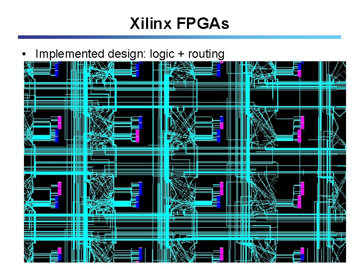
Xilinx FPGAs • Implemented design: logic + routing

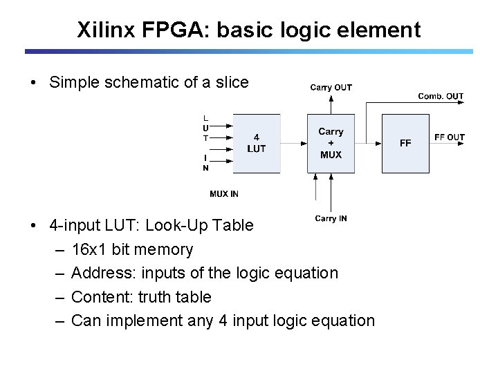
Xilinx FPGAs – CLB • Each CLB consists of 4 slices • Slice: – 2 LUTs: look up table, used to implement • Combinatorial logic functions • Small ROM and RAM • Efficient shift registers – 2 Storage elements: configured to FF or latch • Control signals (set, reset, ce) are shared within a slice – Dedicated multiplexer (MUXFx) – Fast carry logic (MUXCY, XORCY)

Xilinx FPGA: basic logic element • Simple schematic of a slice • 4 -input LUT: Look-Up Table – 16 x 1 bit memory – Address: inputs of the logic equation – Content: truth table – Can implement any 4 input logic equation

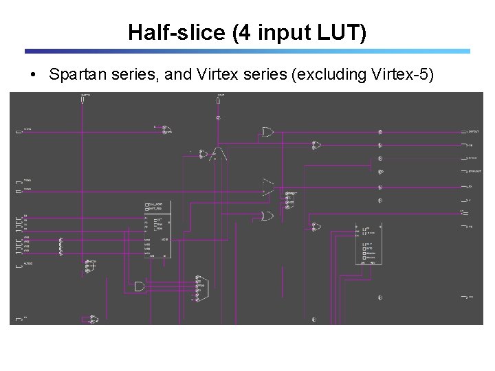
Half-slice (4 input LUT) • Spartan series, and Virtex series (excluding Virtex-5)

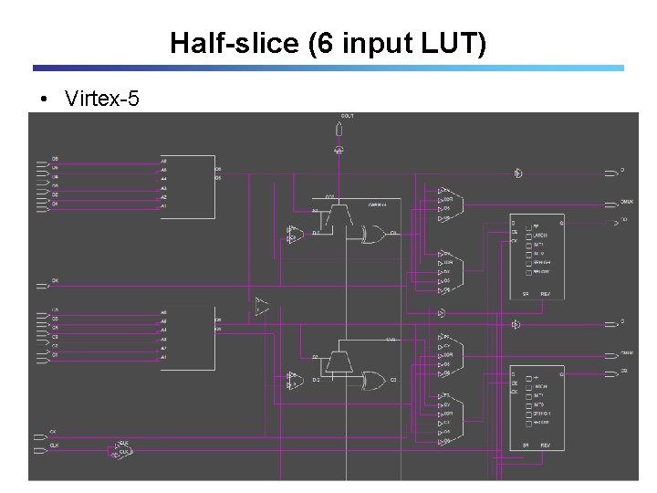
Half-slice (6 input LUT) • Virtex-5
![LUT ROM ROM asynchronous HDL code module rom 16 input 3 0 LUT ROM • ROM (asynchronous) – HDL code module rom 16 (input [3: 0]](https://slidetodoc.com/presentation_image/248aef338f6368e64b32e59b750bf3fa/image-61.jpg)
LUT ROM • ROM (asynchronous) – HDL code module rom 16 (input [3: 0] address, output reg [7: 0] data); always @ (*) case(address) 4’b 0000: data <= CONSTANT 0; 4’b 0001: data <= CONSTANT 1; …… 4’b 1111: data <= CONSTANT 15; endcase endmodule – Xilinx primitives • ROM 16 X 1, ROM 32 x 1, …. .

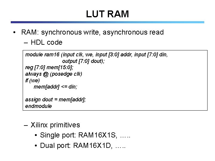
LUT RAM • RAM: synchronous write, asynchronous read – HDL code module ram 16 (input clk, we, input [3: 0] addr, input [7: 0] din, output [7: 0] dout); reg [7: 0] mem[15: 0]; always @ (posedge clk) if (we) mem[addr] <= din; assign dout = mem[addr]; endmodule – Xilinx primitives • Single port: RAM 16 X 1 S, …. . • Dual port: RAM 16 X 1 D, …. .

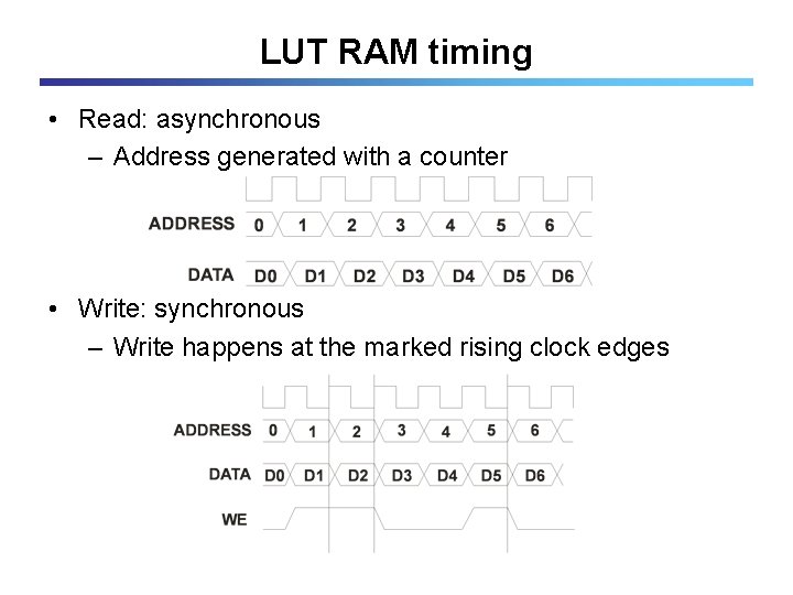
LUT RAM timing • Read: asynchronous – Address generated with a counter • Write: synchronous – Write happens at the marked rising clock edges

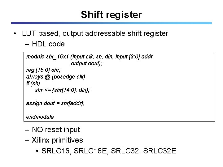
Shift register • LUT based, output addressable shift register – HDL code module shr_16 x 1 (input clk, sh, din, input [3: 0] addr, output dout); reg [15: 0] shr; always @ (posedge clk) if (sh) shr <= {shr[14: 0], din}; assign dout = shr[addr]; endmodule – NO reset input – Xilinx primitives • SRLC 16, SRLC 16 E, SRLC 32 E
![Shift register array module shr16 x 8 input clk sh input 3 0 addr Shift register array module shr_16 x 8 (input clk, sh, input [3: 0] addr,](https://slidetodoc.com/presentation_image/248aef338f6368e64b32e59b750bf3fa/image-65.jpg)
Shift register array module shr_16 x 8 (input clk, sh, input [3: 0] addr, input [7: 0] din, output [7: 0] dout); reg [7: 0] shr[15: 0]; integer i; always @ (posedge clk) if (sh) begin shr[0] <= din; for (i=15; i>0, i=i-1) begin shr[i] <= shr[i-1]; end assign dout = shr[addr]; endmodule

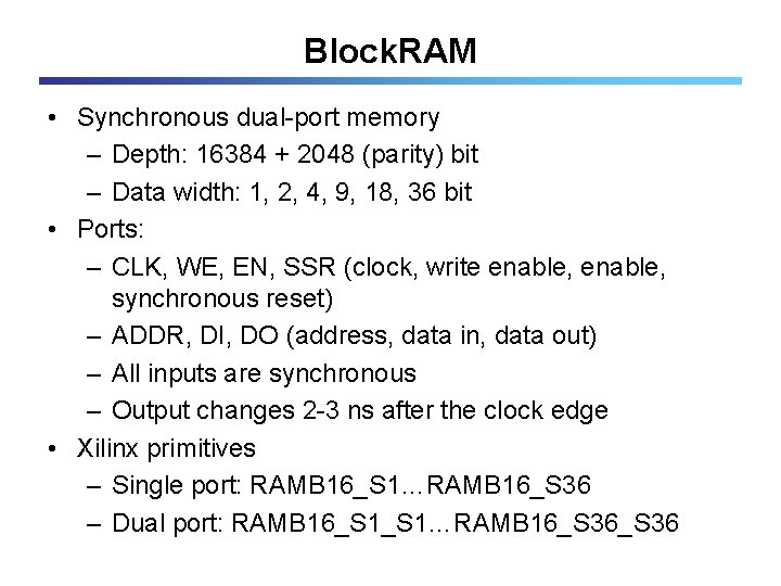
Block. RAM • Synchronous dual-port memory – Depth: 16384 + 2048 (parity) bit – Data width: 1, 2, 4, 9, 18, 36 bit • Ports: – CLK, WE, EN, SSR (clock, write enable, synchronous reset) – ADDR, DI, DO (address, data in, data out) – All inputs are synchronous – Output changes 2 -3 ns after the clock edge • Xilinx primitives – Single port: RAMB 16_S 1…RAMB 16_S 36 – Dual port: RAMB 16_S 1…RAMB 16_S 36

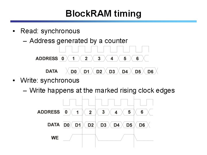
Block. RAM timing • Read: synchronous – Address generated by a counter • Write: synchronous – Write happens at the marked rising clock edges

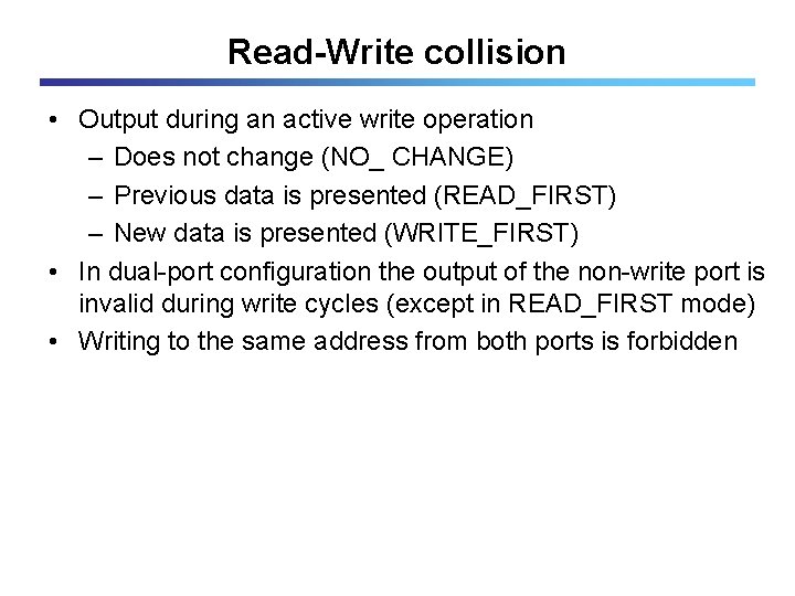
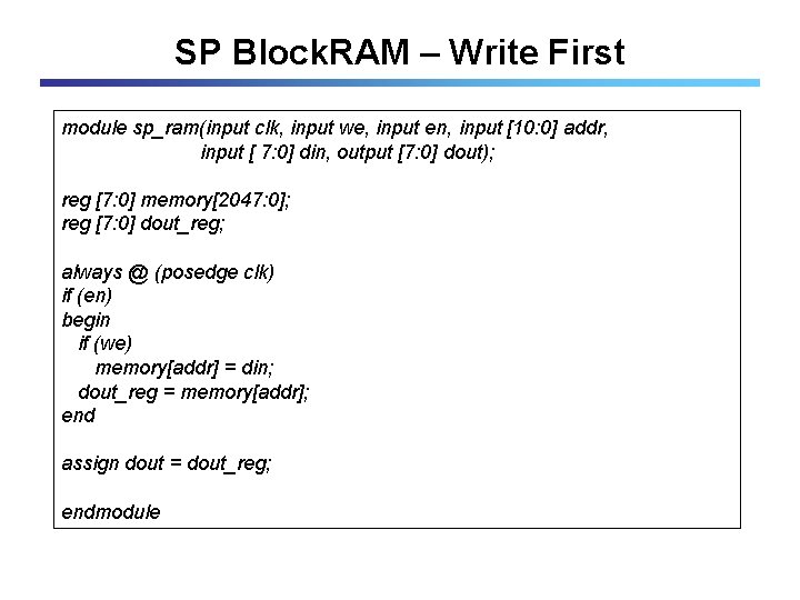
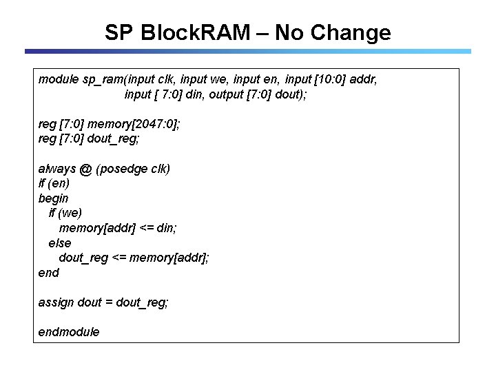
Read-Write collision • Output during an active write operation – Does not change (NO_ CHANGE) – Previous data is presented (READ_FIRST) – New data is presented (WRITE_FIRST) • In dual-port configuration the output of the non-write port is invalid during write cycles (except in READ_FIRST mode) • Writing to the same address from both ports is forbidden

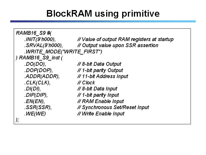
Block. RAM using primitive RAMB 16_S 9 #(. INIT(9'h 000), // Value of output RAM registers at startup. SRVAL(9'h 000), // Output value upon SSR assertion. WRITE_MODE("WRITE_FIRST") ) RAMB 16_S 9_inst (. DO(DO), // 8 -bit Data Output. DOP(DOP), // 1 -bit parity Output. ADDR(ADDR), // 11 -bit Address Input. CLK(CLK), // Clock. DI(DI), // 8 -bit Data Input. DIP(DIP), // 1 -bit parity Input. EN(EN), // RAM Enable Input. SSR(SSR), // Synchronous Set/Reset Input. WE(WE) // Write Enable Input );

SP Block. RAM – Read First module sp_ram(input clk, input we, input en, input [10: 0] addr, input [ 7: 0] din, output [7: 0] dout); reg [7: 0] memory[2047: 0]; reg [7: 0] dout_reg; always @ (posedge clk) if (en) begin if (we) memory[addr] <= din; dout_reg <= memory[addr]; end assign dout = dout_reg; endmodule

SP Block. RAM – Write First module sp_ram(input clk, input we, input en, input [10: 0] addr, input [ 7: 0] din, output [7: 0] dout); reg [7: 0] memory[2047: 0]; reg [7: 0] dout_reg; always @ (posedge clk) if (en) begin if (we) memory[addr] = din; dout_reg = memory[addr]; end assign dout = dout_reg; endmodule

SP Block. RAM – No Change module sp_ram(input clk, input we, input en, input [10: 0] addr, input [ 7: 0] din, output [7: 0] dout); reg [7: 0] memory[2047: 0]; reg [7: 0] dout_reg; always @ (posedge clk) if (en) begin if (we) memory[addr] <= din; else dout_reg <= memory[addr]; end assign dout = dout_reg; endmodule
![DP Block RAM module dpraminput clka wea ena clkb web enb input 10 0 DP Block. RAM module dp_ram(input clk_a, we_a, en_a, clk_b, we_b, en_b, input [10: 0]](https://slidetodoc.com/presentation_image/248aef338f6368e64b32e59b750bf3fa/image-73.jpg)
DP Block. RAM module dp_ram(input clk_a, we_a, en_a, clk_b, we_b, en_b, input [10: 0] addr_a, addr_b, input [ 7: 0] din_a, din_b, output [7: 0] dout_a, dout_b); reg [7: 0] memory[2047: 0]; reg [7: 0] dout_reg_a, dout_reg_b; always @ (posedge clk_a) if (en_a) begin if (we_a) memory[addr_a] <= din_a; dout_reg_a <= memory[addr_a]; end assign dout_a = dout_reg_a; always @ (posedge clk_b) if (en_b) begin if (we_b) memory[addr_b] <= din_b; dout_reg_b <= memory[addr_b]; end assign dout_b = dout_reg_b; endmodule

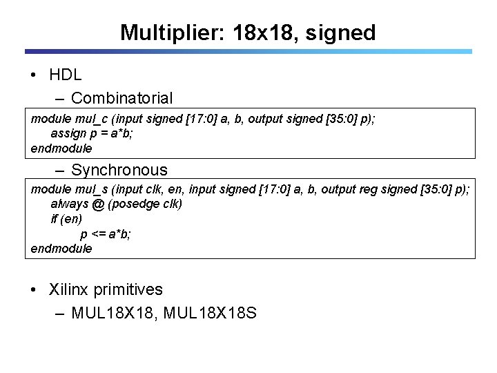
Multiplier: 18 x 18, signed • HDL – Combinatorial module mul_c (input signed [17: 0] a, b, output signed [35: 0] p); assign p = a*b; endmodule – Synchronous module mul_s (input clk, en, input signed [17: 0] a, b, output reg signed [35: 0] p); always @ (posedge clk) if (en) p <= a*b; endmodule • Xilinx primitives – MUL 18 X 18, MUL 18 X 18 S