Verilog for Digital Design Chapter 5 RTL Design


![High-Level State Machine Behavior • . . . Comb. Logic process reg [0: 0] High-Level State Machine Behavior • . . . Comb. Logic process reg [0: 0]](https://slidetodoc.com/presentation_image/3445e84bc32449840c7fe4f3282bca91/image-5.jpg)



- Slides: 45

Verilog for Digital Design Chapter 5: RTL Design Verilog for Digital Design Copyright © 2007 Frank Vahid and Roman Lysecky 1

High-Level State Machine Behavior Verilog for Digital Design Copyright © 2007 Frank Vahid and Roman Lysecky 2

High-Level State Machine Behavior • Register-transfer level (RTL) design captures desired system behavior using high-level state machine – Earlier example – 3 cycles high, used FSM – What if 512 cycles high? 512 -state FSM? – Better solution – High-level state machine that uses register to count cycles • Declare explicit register Cnt (2 bits for 3 cycles high) • Initialize Cnt to 2 (2, 1, 0 3 counts) • "On" state – – Sets X=1 Configures Cnt for decrement on next cycle Transitions to Off when Cnt is 0 Note that transition conditions use current value of Cnt, not next (decremented) value • For 512 cycles high, just initialize Cnt to 511 Verilog for Digital Design Copyright © 2007 Frank Vahid and Roman Lysecky Inputs: B; Outputs: X X=0 Off B B' X=1 X=1 On 2 On 3 3 cycles with X=1 Inputs: B; Outputs: X; Register: Cnt(2) X=0 Cnt=2 Off B B' Cnt=0 X=1 Cnt=Cnt-1 On (Cnt=0)' 3 cycles with X=1 3

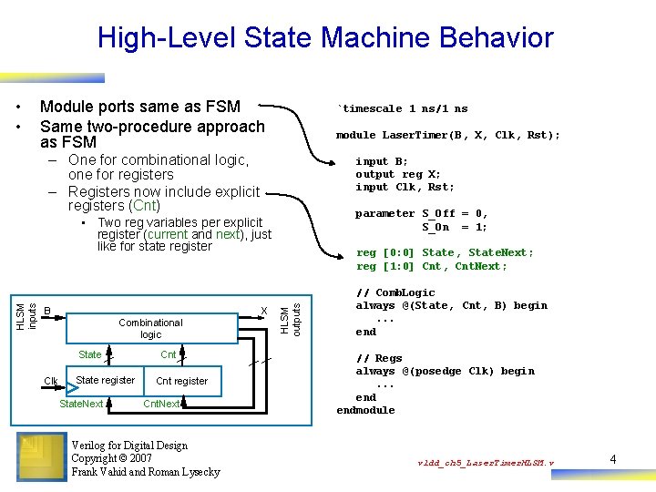
High-Level State Machine Behavior • • Module ports same as FSM Same two-procedure approach as FSM `timescale 1 ns/1 ns module Laser. Timer(B, X, Clk, Rst); – One for combinational logic, one for registers – Registers now include explicit registers (Cnt) input B; output reg X; input Clk, Rst; parameter S_Off = 0, S_On = 1; x Combinational logic State Clk clk Stateregister State. Next Cnt register Cnt. Next Verilog for Digital Design Copyright © 2007 Frank Vahid and Roman Lysecky X reg [0: 0] State, State. Next; reg [1: 0] Cnt, Cnt. Next; HLSM outputs b. B FSM outputs FSM HLSM inputs • Two reg variables per explicit register (current and next), just like for state register // Comb. Logic always @(State, Cnt, B) begin. . . end // Regs always @(posedge Clk) begin. . . endmodule vldd_ch 5_Laser. Timer. HLSM. v 4
![HighLevel State Machine Behavior Comb Logic process reg 0 0 High-Level State Machine Behavior • . . . Comb. Logic process reg [0: 0]](https://slidetodoc.com/presentation_image/3445e84bc32449840c7fe4f3282bca91/image-5.jpg)
High-Level State Machine Behavior • . . . Comb. Logic process reg [0: 0] State, State. Next; reg [1: 0] Cnt, Cnt. Next; – Describes actions and transitions // Comb. Logic always @(State, Cnt, B) begin case (State) S_Off: begin X <= 0; Cnt. Next <= 2; if (B == 0) State. Next <= S_Off; else State. Next <= S_On; end S_On: begin X <= 1; Cnt. Next <= Cnt - 1; if (Cnt == 0) State. Next <= S_Off; else State. Next <= S_On; endcase end Inputs: B; Outputs: X; Register: Cnt(2) X=0 Cnt=2 Off X=1 Cnt=Cnt-1 HLSM inputs On Cnt=0 (Cnt=0)' X B Combinational logic State Clk State register State. Next HLSM outputs B B' Cnt register Cnt. Next Verilog for Digital Design Copyright © 2007 Frank Vahid and Roman Lysecky Note: Writes are to "next" variable, reads are from "current" variable. See target architecture to understand why. . vldd_ch 5_Laser. Timer. HLSM. v 5

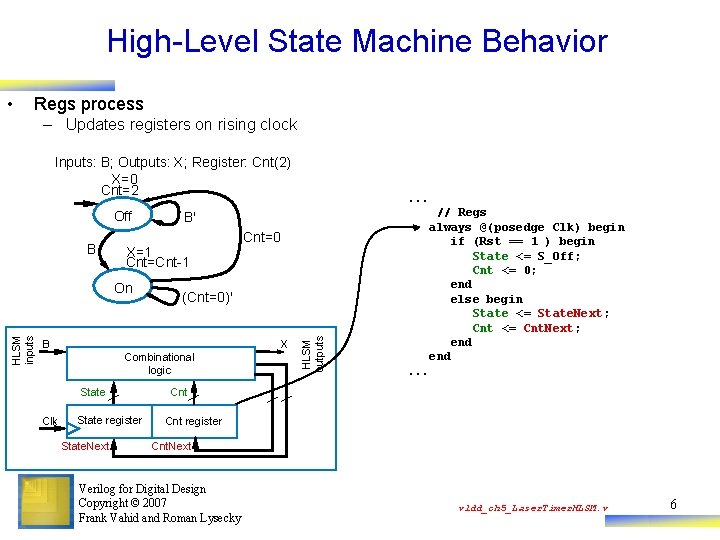
High-Level State Machine Behavior • Regs process – Updates registers on rising clock Inputs: B; Outputs: X; Register: Cnt(2) X=0 Cnt=2 B X=1 Cnt=Cnt-1 HLSM inputs On X Combinational logic Clk Cnt=0 (Cnt=0)' B State register State. Next // Regs always @(posedge Clk) begin if (Rst == 1 ) begin State <= S_Off; Cnt <= 0; end else begin State <= State. Next; Cnt <= Cnt. Next; end B' HLSM outputs Off . . . Cnt register Cnt. Next Verilog for Digital Design Copyright © 2007 Frank Vahid and Roman Lysecky vldd_ch 5_Laser. Timer. HLSM. v 6

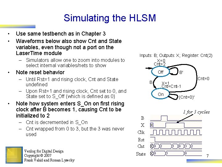
Simulating the HLSM • • Use same testbench as in Chapter 3 Waveforms below also show Cnt and State variables, even though not a port on the Laser. Time module – Simulators allow one to zoom into modules to select internal variables/nets to show • Inputs: B; Outputs: X; Register: Cnt(2) X=0 Cnt=2 Note reset behavior Off – Until Rst=1 and rising clock, Cnt and State undefined – Upon Rst=1 and rising clock, Cnt set to 0, and State set to S_Off (which is defined as 0) • Note how system enters S_On on first rising clock after B becomes 1, causing Cnt to be initialized to 2 – Cnt is decremented in S_On – Cnt wrapped from 0 to 3, but the 3 was never used Verilog for Digital Design Copyright © 2007 Frank Vahid and Roman Lysecky B B' Cnt=0 X=1 Cnt=Cnt-1 On (Cnt=0)' 1 for 3 cycles B X Clk Rst Cnt X State X x 7

Top-Down Design— HLSM to Controller and Datapath Verilog for Digital Design Copyright © 2007 Frank Vahid and Roman Lysecky 8

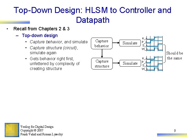
Top-Down Design: HLSM to Controller and Datapath • Recall from Chapters 2 & 3 – Top-down design • Capture behavior, and simulate • Capture structure (circuit), simulate again • Gets behavior right first, unfettered by complexity of creating structure Verilog for Digital Design Copyright © 2007 Frank Vahid and Roman Lysecky Capture behavior Capture structure Simulate K_s P_s S_s W_s Should be the same 9

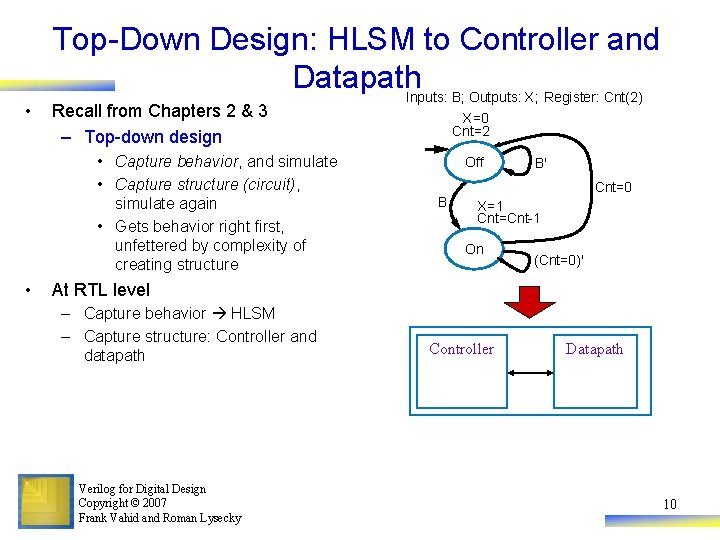
• Top-Down Design: HLSM to Controller and Datapath Inputs: B; Outputs: X; Register: Cnt(2) Recall from Chapters 2 & 3 – Top-down design • Capture behavior, and simulate • Capture structure (circuit), simulate again • Gets behavior right first, unfettered by complexity of creating structure • X=0 Cnt=2 Off B B' Cnt=0 X=1 Cnt=Cnt-1 On (Cnt=0)' At RTL level – Capture behavior HLSM – Capture structure: Controller and datapath Verilog for Digital Design Copyright © 2007 Frank Vahid and Roman Lysecky Controller Datapath 10

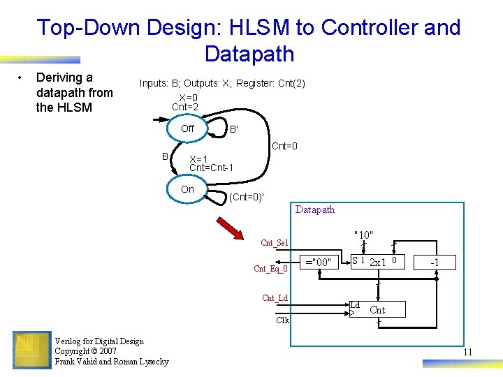
Top-Down Design: HLSM to Controller and Datapath • Deriving a datapath from the HLSM Inputs: B; Outputs: X; Register: Cnt(2) X=0 Cnt=2 Off B B' Cnt=0 X=1 Cnt=Cnt-1 On (Cnt=0)' Datapath "10" Cnt_Sel Cnt_Eq_0 Cnt_Ld Clk Verilog for Digital Design Copyright © 2007 Frank Vahid and Roman Lysecky ="00" S 1 2 x 1 0 Ld -1 Cnt 11

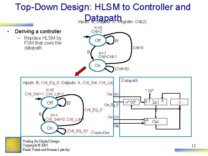
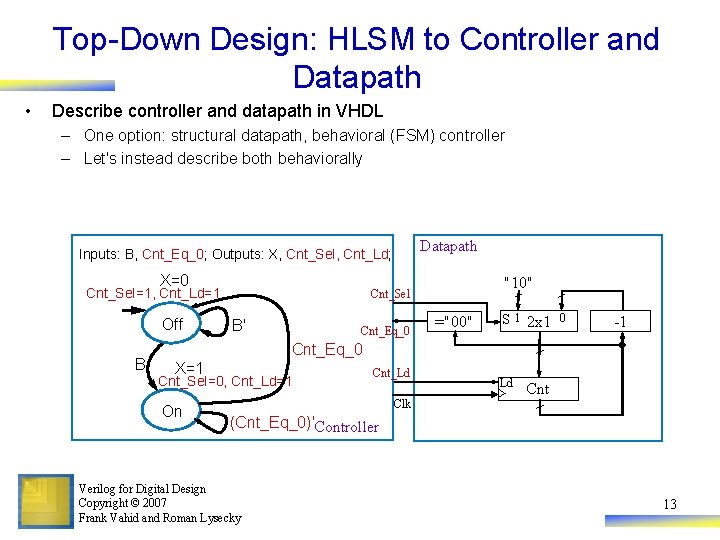
Top-Down Design: HLSM to Controller and Datapath Inputs: B; Outputs: X; Register: Cnt(2) • X=0 Cnt=2 Deriving a controller – Replace HLSM by FSM that uses the datapath Off B B' Cnt=0 X=1 Cnt=Cnt-1 On (Cnt=0)' Datapath Inputs: B, Cnt_Eq_0; Outputs: X, Cnt_Sel, Cnt_Ld; X=0 Cnt_Sel=1, Cnt_Ld=1 Off B "10" Cnt_Sel B' Cnt_Eq_0 ="00" S 1 2 x 1 0 -1 Cnt_Eq_0 X=1 Cnt_Sel=0, Cnt_Ld=1 On Cnt_Ld Clk Ld Cnt (Cnt_Eq_0)' Controller Verilog for Digital Design Copyright © 2007 Frank Vahid and Roman Lysecky 12

Top-Down Design: HLSM to Controller and Datapath • Describe controller and datapath in VHDL – One option: structural datapath, behavioral (FSM) controller – Let's instead describe both behaviorally Datapath Inputs: B, Cnt_Eq_0; Outputs: X, Cnt_Sel, Cnt_Ld; X=0 Cnt_Sel=1, Cnt_Ld=1 Off B "10" Cnt_Sel B' Cnt_Eq_0 ="00" S 1 2 x 1 0 -1 Cnt_Eq_0 X=1 Cnt_Sel=0, Cnt_Ld=1 On Cnt_Ld Clk Ld Cnt (Cnt_Eq_0)'Controller Verilog for Digital Design Copyright © 2007 Frank Vahid and Roman Lysecky 13

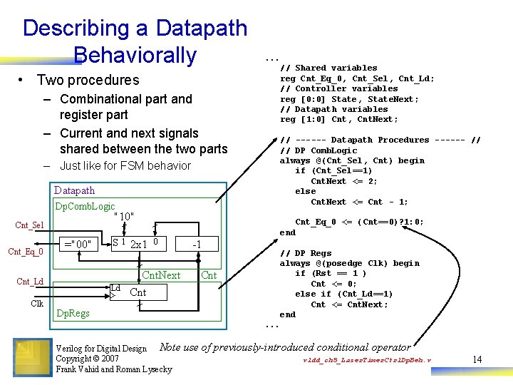
Describing a Datapath Behaviorally . . . // Shared variables reg Cnt_Eq_0, Cnt_Sel, Cnt_Ld; // Controller variables reg [0: 0] State, State. Next; // Datapath variables reg [1: 0] Cnt, Cnt. Next; • Two procedures – Combinational part and register part – Current and next signals shared between the two parts // ------ Datapath Procedures ------ // // DP Comb. Logic always @(Cnt_Sel, Cnt) begin if (Cnt_Sel==1) Cnt. Next <= 2; else Cnt. Next <= Cnt - 1; – Just like for FSM behavior Datapath Dp. Comb. Logic "10" Cnt_Sel Cnt_Eq_0 ="00" 2 x 1 0 Cnt. Next Cnt_Ld Clk S 1 Cnt_Eq_0 <= (Cnt==0)? 1: 0; Ld end -1 // DP Regs always @(posedge Clk) begin if (Rst == 1 ) Cnt <= 0; else if (Cnt_Ld==1) Cnt <= Cnt. Next; end Cnt Dp. Regs. . . Verilog for Digital Design Note Copyright © 2007 Frank Vahid and Roman Lysecky use of previously-introduced conditional operator vldd_ch 5_Laser. Timer. Ctrl. Dp. Beh. v 14

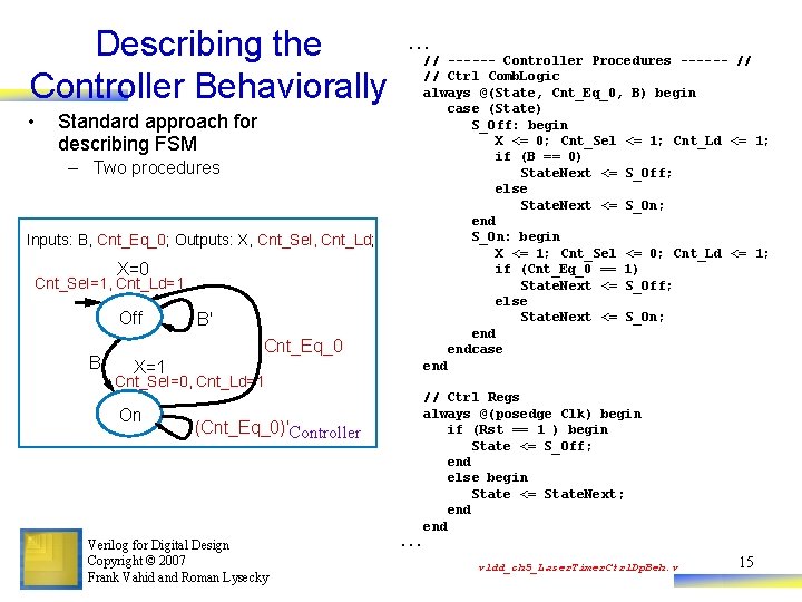
Describing the Controller Behaviorally • Standard approach for describing FSM – Two procedures Inputs: B, Cnt_Eq_0; Outputs: X, Cnt_Sel, Cnt_Ld; X=0 Cnt_Sel=1, Cnt_Ld=1 Off B B' Cnt_Eq_0 X=1 Cnt_Sel=0, Cnt_Ld=1 On . . . // ------ Controller Procedures ------ // // Ctrl Comb. Logic always @(State, Cnt_Eq_0, B) begin case (State) S_Off: begin X <= 0; Cnt_Sel <= 1; Cnt_Ld <= 1; if (B == 0) State. Next <= S_Off; else State. Next <= S_On; end S_On: begin X <= 1; Cnt_Sel <= 0; Cnt_Ld <= 1; if (Cnt_Eq_0 == 1) State. Next <= S_Off; else State. Next <= S_On; endcase end // Ctrl Regs always @(posedge Clk) begin if (Rst == 1 ) begin State <= S_Off; end else begin State <= State. Next; end (Cnt_Eq_0)'Controller Verilog for Digital Design Copyright © 2007 Frank Vahid and Roman Lysecky . . . vldd_ch 5_Laser. Timer. Ctrl. Dp. Beh. v 15

Controller and Datapath Behavior • Result is one module with four procedures • Combinational logic • Registers – Controller procedures (2) // ------ Datapath Procedures ------ // // DP Comb. Logic always @(Cnt_Sel, Cnt) begin. . . end • Combinational logic • Registers X=0 Cnt_Sel=1, Cnt_Ld=1 Off B' "10" Cnt_Eq_0 ="00" S 1 2 x 1 0 Cnt_Eq_0 B X=1 Cnt_Sel=0, Cnt_Ld=1 On // DP Regs always @(posedge Clk) begin. . . end Datapath Cnt_Se l Cnt_Ld Ld Clk (Cnt_Eq_0)' Controller Verilog for Digital Design Copyright © 2007 Frank Vahid and Roman Lysecky Cnt parameter S_Off = 0, S_On = 1; // Shared variables reg Cnt_Eq_0, Cnt_Sel, Cnt_Ld; // Controller variables reg [0: 0] State, State. Next; // Datapath variables reg [1: 0] Cnt, Cnt. Next; – Datapath procedures (2) Inputs: B, Cnt_Eq_0; Outputs: X, Cnt_Sel, Cnt_Ld; . . . module Laser. Timer(B, X, Clk, Rst); . . . -1 // ------ Controller Procedures ------ // // Ctrl Comb. Logic always @(State, Cnt_Eq_0, B) begin. . . end // Ctrl Regs always @(posedge Clk) begin. . . end vldd_ch 5_Laser. Timer. Ctrl. Dp. Beh. v endmodule 16

Describing a State Machine using One Process Verilog for Digital Design Copyright © 2007 Frank Vahid and Roman Lysecky 17

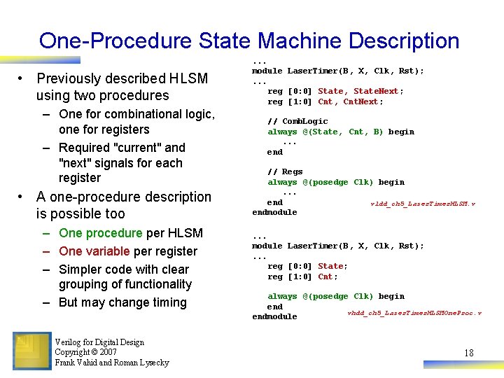
One-Procedure State Machine Description • Previously described HLSM using two procedures – One for combinational logic, one for registers – Required "current" and "next" signals for each register • A one-procedure description is possible too – One procedure per HLSM – One variable per register – Simpler code with clear grouping of functionality – But may change timing Verilog for Digital Design Copyright © 2007 Frank Vahid and Roman Lysecky . . . module Laser. Timer(B, X, Clk, Rst); . . . reg [0: 0] State, State. Next; reg [1: 0] Cnt, Cnt. Next; // Comb. Logic always @(State, Cnt, B) begin. . . end // Regs always @(posedge Clk) begin. . . end vldd_ch 5_Laser. Timer. HLSM. v endmodule. . . module Laser. Timer(B, X, Clk, Rst); . . . reg [0: 0] State; reg [1: 0] Cnt; always @(posedge Clk) begin end vhdd_ch 5_Laser. Timer. HLSMOne. Proc. v endmodule 18

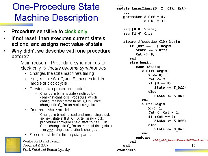
One-Procedure State Machine Description • • • Procedure sensitive to clock only If not reset, then executes current state's actions, and assigns next value of state Why didn't we describe with one procedure before? – Main reason – Procedure synchronous to clock only Inputs become synchronous • Changes the state machine's timing • e. g. , In state S_off, and B changes to 1 in middle of clock cycle • Previous two procedure model – Change in b immediately noticed by combinational logic procedure, which configures next state to be S_On. State changes to S_On on next rising clock. • One procedure model – Change in b noticed until next rising clock, so next state still S_Off. After rising clock, procedure configures next state to be S_On. State changes to S_On on the next rising clock – or two rising clocks after b changed • See next slide for timing diagrams Verilog for Digital Design Copyright © 2007 Frank Vahid and Roman Lysecky . . . module Laser. Timer(B, X, Clk, Rst); . . . parameter S_Off = 0, S_On = 1; reg [0: 0] State; reg [1: 0] Cnt; always @(posedge Clk) begin if (Rst == 1 ) begin State <= S_Off; Cnt <= 0; end else begin case (State) S_Off: begin X <= 0; Cnt <= 2; if (B == 0) State <= S_Off; else State <= S_On; end S_On: begin X <= 1; Cnt <= Cnt - 1; if (Cnt == 0) State <= S_Off; else State <= S_On; endcase vldd_ch 5_Laser. Timer. HLSMOne. Proc. v end 19 endmodule

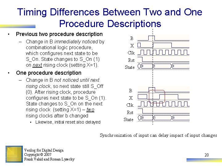
Timing Differences Between Two and One Procedure Descriptions • Previous two procedure description – Change in B immediately noticed by combinational logic procedure, which configures next state to be S_On. State changes to S_On (1) on next rising clock (setting X=1). • One procedure description – Change in B noticed until next rising clock, so next state still S_Off (0). After rising clock, procedure configures next state to be S_On (1). State changes to S_On on the next rising clock (setting X=1) – two rising clocks after b changed • Likewise, initial reset also delayed B X Clk Rst State Synchronization of input can delay impact of input changes Verilog for Digital Design Copyright © 2007 Frank Vahid and Roman Lysecky 20

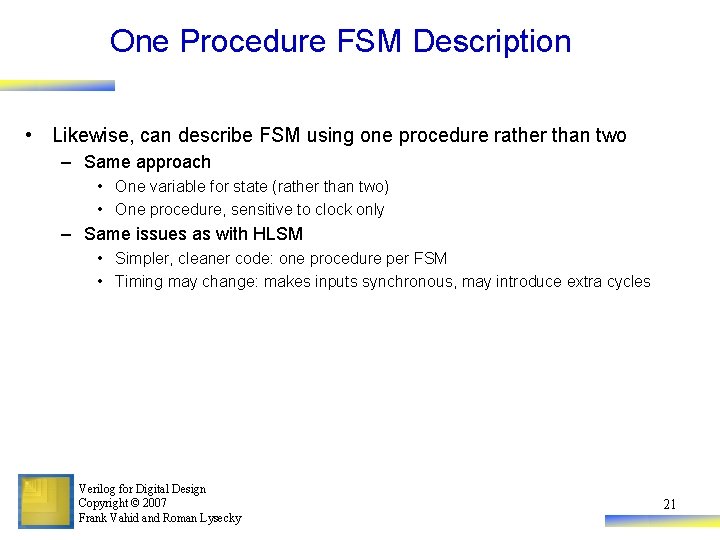
One Procedure FSM Description • Likewise, can describe FSM using one procedure rather than two – Same approach • One variable for state (rather than two) • One procedure, sensitive to clock only – Same issues as with HLSM • Simpler, cleaner code: one procedure per FSM • Timing may change: makes inputs synchronous, may introduce extra cycles Verilog for Digital Design Copyright © 2007 Frank Vahid and Roman Lysecky 21

Improving Timing Realism Verilog for Digital Design Copyright © 2007 Frank Vahid and Roman Lysecky 22

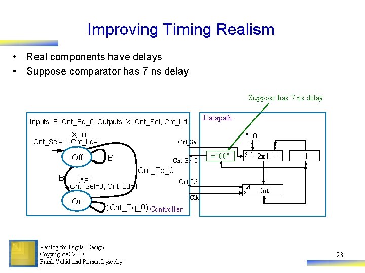
Improving Timing Realism • Real components have delays • Suppose comparator has 7 ns delay Suppose has 7 ns delay Datapath Inputs: B, Cnt_Eq_0; Outputs: X, Cnt_Sel, Cnt_Ld; X=0 Cnt_Sel=1, Cnt_Ld=1 Off B "10" Cnt_Sel B' Cnt_Eq_0 ="00" S 1 2 x 1 0 -1 Cnt_Eq_0 X=1 Cnt_Sel=0, Cnt_Ld=1 On Cnt_Ld Clk Ld Cnt (Cnt_Eq_0)'Controller Verilog for Digital Design Copyright © 2007 Frank Vahid and Roman Lysecky 23

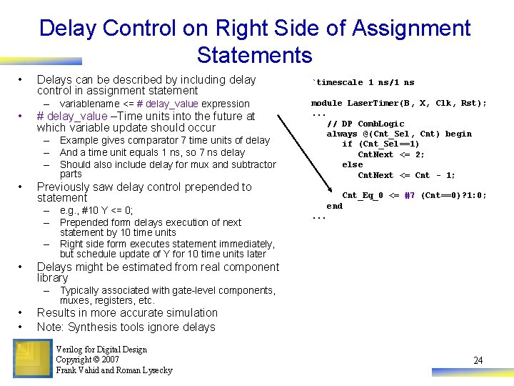
Delay Control on Right Side of Assignment Statements • Delays can be described by including delay control in assignment statement – variablename <= # delay_value expression • # delay_value –Time units into the future at which variable update should occur – Example gives comparator 7 time units of delay – And a time unit equals 1 ns, so 7 ns delay – Should also include delay for mux and subtractor parts • module Laser. Timer(B, X, Clk, Rst); . . . // DP Comb. Logic always @(Cnt_Sel, Cnt) begin if (Cnt_Sel==1) Cnt. Next <= 2; else Cnt. Next <= Cnt - 1; Previously saw delay control prepended to statement – e. g. , #10 Y <= 0; – Prepended form delays execution of next statement by 10 time units – Right side form executes statement immediately, but schedule update of Y for 10 time units later • `timescale 1 ns/1 ns Cnt_Eq_0 <= #7 (Cnt==0)? 1: 0; end. . . Delays might be estimated from real component library – Typically associated with gate-level components, muxes, registers, etc. • • Results in more accurate simulation Note: Synthesis tools ignore delays Verilog for Digital Design Copyright © 2007 Frank Vahid and Roman Lysecky 24

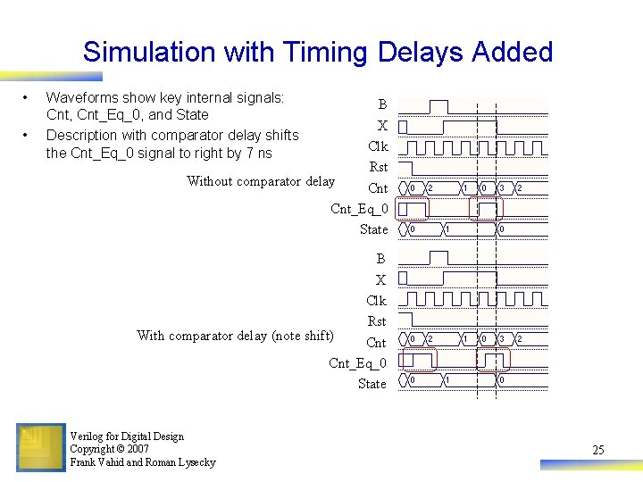
Simulation with Timing Delays Added • • Waveforms show key internal signals: Cnt, Cnt_Eq_0, and State Description with comparator delay shifts the Cnt_Eq_0 signal to right by 7 ns B X Clk Rst Without comparator delay Cnt_Eq_0 State B X Clk Rst With comparator delay (note shift) Cnt_Eq_0 State Verilog for Digital Design Copyright © 2007 Frank Vahid and Roman Lysecky 25

Algorithmic-Level Behavior Verilog for Digital Design Copyright © 2007 Frank Vahid and Roman Lysecky 26

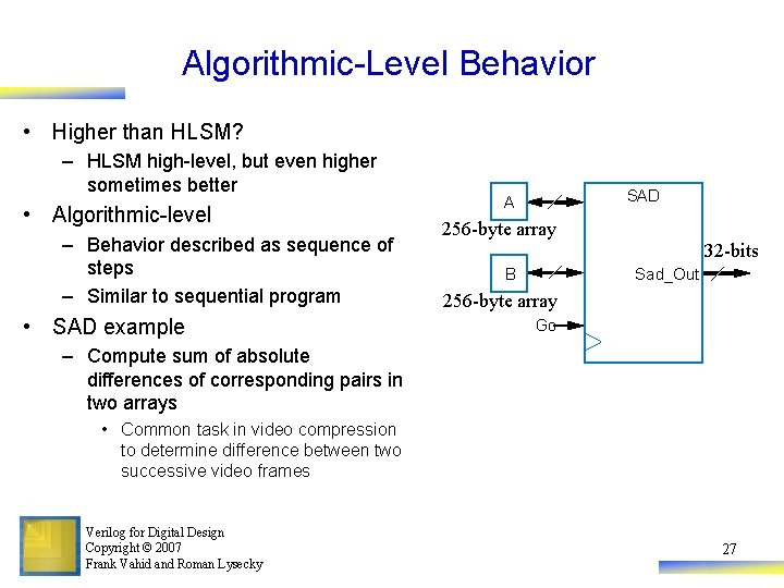
Algorithmic-Level Behavior • Higher than HLSM? – HLSM high-level, but even higher sometimes better • Algorithmic-level – Behavior described as sequence of steps – Similar to sequential program • SAD example SAD A 256 -byte array B 32 -bits Sad_Out 256 -byte array Go – Compute sum of absolute differences of corresponding pairs in two arrays • Common task in video compression to determine difference between two successive video frames Verilog for Digital Design Copyright © 2007 Frank Vahid and Roman Lysecky 27

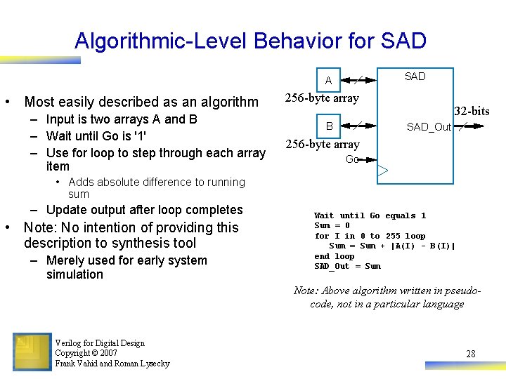
Algorithmic-Level Behavior for SAD A • Most easily described as an algorithm – Input is two arrays A and B – Wait until Go is '1' – Use for loop to step through each array item 256 -byte array B 32 -bits SAD_Out 256 -byte array Go • Adds absolute difference to running sum – Update output after loop completes • Note: No intention of providing this description to synthesis tool – Merely used for early system simulation Wait until Go equals 1 Sum = 0 for I in 0 to 255 loop Sum = Sum + |A(I) - B(I)| end loop SAD_Out = Sum Note: Above algorithm written in pseudocode, not in a particular language Verilog for Digital Design Copyright © 2007 Frank Vahid and Roman Lysecky 28

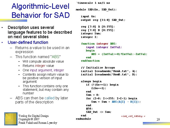
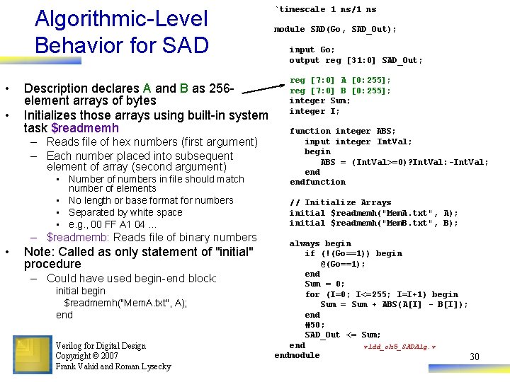
Algorithmic-Level Behavior for SAD • • Description uses several language features to be described on next several slides User-defined function – Returns a value to be used in an expression – This function named "ABS" • • Will compute absolute value Returns integer value One input argument, integer Contents assign return value to be positive version of input argument • This function contains only one statement, but may contain any number – ABS can then be called by later parts of the description Verilog for Digital Design Copyright © 2007 Frank Vahid and Roman Lysecky `timescale 1 ns/1 ns module SAD(Go, SAD_Out); input Go; output reg [31: 0] SAD_Out; reg [7: 0] A [0: 255]; reg [7: 0] B [0: 255]; integer Sum; integer I; function integer ABS; input integer Int. Val; begin ABS = (Int. Val>=0)? Int. Val: -Int. Val; endfunction // Initialize Arrays initial $readmemh("Mem. A. txt", A); initial $readmemh("Mem. B. txt", B); always begin if (!(Go==1)) begin @(Go==1); end Sum = 0; for (I=0; I<=255; I=I+1) begin Sum = Sum + ABS(A[I] - B[I]); end #50; SAD_Out <= Sum; end vldd_ch 5_SADAlg. v endmodule 29

Algorithmic-Level Behavior for SAD • • Description declares A and B as 256 element arrays of bytes Initializes those arrays using built-in system task $readmemh – Reads file of hex numbers (first argument) – Each number placed into subsequent element of array (second argument) • Number of numbers in file should match number of elements • No length or base format for numbers • Separated by white space • e. g. , 00 FF A 1 04. . . – $readmemb: Reads file of binary numbers • Note: Called as only statement of "initial" procedure – Could have used begin-end block: initial begin $readmemh("Mem. A. txt", A); end Verilog for Digital Design Copyright © 2007 Frank Vahid and Roman Lysecky `timescale 1 ns/1 ns module SAD(Go, SAD_Out); input Go; output reg [31: 0] SAD_Out; reg [7: 0] A [0: 255]; reg [7: 0] B [0: 255]; integer Sum; integer I; function integer ABS; input integer Int. Val; begin ABS = (Int. Val>=0)? Int. Val: -Int. Val; endfunction // Initialize Arrays initial $readmemh("Mem. A. txt", A); initial $readmemh("Mem. B. txt", B); always begin if (!(Go==1)) begin @(Go==1); end Sum = 0; for (I=0; I<=255; I=I+1) begin Sum = Sum + ABS(A[I] - B[I]); end #50; SAD_Out <= Sum; end vldd_ch 5_SADAlg. v endmodule 30

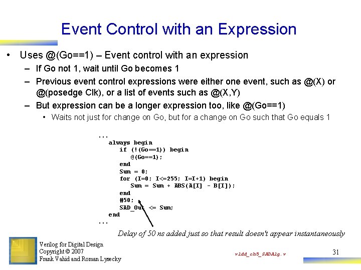
Event Control with an Expression • Uses @(Go==1) – Event control with an expression – If Go not 1, wait until Go becomes 1 – Previous event control expressions were either one event, such as @(X) or @(posedge Clk), or a list of events such as @(X, Y) – But expression can be a longer expression too, like @(Go==1) • Waits not just for change on Go, but for a change on Go such that Go equals 1. . . always begin if (!(Go==1)) begin @(Go==1); end Sum = 0; for (I=0; I<=255; I=I+1) begin Sum = Sum + ABS(A[I] - B[I]); end #50; SAD_Out <= Sum; end. . . Delay of 50 ns added just so that result doesn't appear instantaneously Verilog for Digital Design Copyright © 2007 Frank Vahid and Roman Lysecky vldd_ch 5_SADAlg. v 31

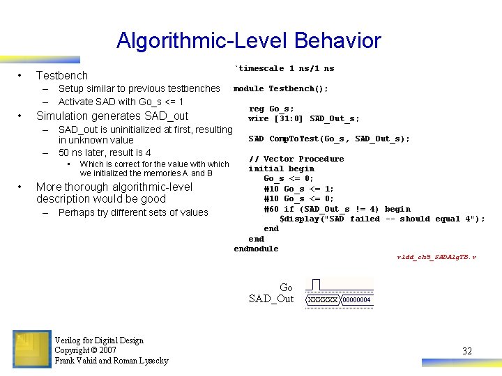
Algorithmic-Level Behavior • Testbench – Setup similar to previous testbenches – Activate SAD with Go_s <= 1 • Simulation generates SAD_out – SAD_out is uninitialized at first, resulting in unknown value – 50 ns later, result is 4 • • Which is correct for the value with which we initialized the memories A and B More thorough algorithmic-level description would be good – Perhaps try different sets of values `timescale 1 ns/1 ns module Testbench(); reg Go_s; wire [31: 0] SAD_Out_s; SAD Comp. To. Test(Go_s, SAD_Out_s); // Vector Procedure initial begin Go_s <= 0; #10 Go_s <= 1; #10 Go_s <= 0; #60 if (SAD_Out_s != 4) begin $display("SAD failed -- should equal 4"); end endmodule vldd_ch 5_SADAlg. TB. v Go SAD_Out Verilog for Digital Design Copyright © 2007 Frank Vahid and Roman Lysecky xxxxxx 32

Top-Down Design – Converting Algorithmic-Level Behavior to RTL Verilog for Digital Design Copyright © 2007 Frank Vahid and Roman Lysecky 33

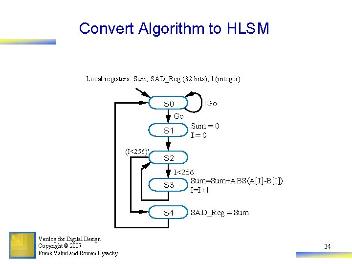
Convert Algorithm to HLSM Local registers: Sum, SAD_Reg (32 bits); I (integer) S 0 Go S 1 (I<256)’ !Go Sum = 0 I=0 S 2 I<256 Sum=Sum+ABS(A[I]-B[I]) S 3 I=I+1 S 4 Verilog for Digital Design Copyright © 2007 Frank Vahid and Roman Lysecky SAD_Reg = Sum 34

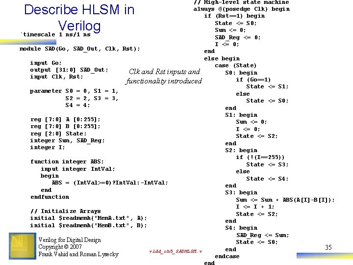
// High-level state machine always @(posedge Clk) begin if (Rst==1) begin State <= S 0; Sum <= 0; `timescale 1 ns/1 ns SAD_Reg <= 0; I <= 0; module SAD(Go, SAD_Out, Clk, Rst); end else begin input Go; case (State) output [31: 0] SAD_Out; Clk and Rst inputs and S 0: begin input Clk, Rst; if (Go==1) functionality introduced State <= S 1; parameter S 0 = 0, S 1 = 1, else S 2 = 2, S 3 = 3, State <= S 0; S 4 = 4; end S 1: begin reg [7: 0] A [0: 255]; Sum <= 0; reg [7: 0] B [0: 255]; I <= 0; reg [2: 0] State; State <= S 2; integer Sum, SAD_Reg; end integer I; S 2: begin if (!(I==255)) function integer ABS; State <= S 3; input integer Int. Val; else begin State <= S 4; ABS = (Int. Val>=0)? Int. Val: -Int. Val; end S 3: begin endfunction Sum <= Sum + ABS(A[I]-B[I]); I <= I + 1; // Initialize Arrays State <= S 2; initial $readmemh("Mem. A. txt", A); end initial $readmemh("Mem. B. txt", B); S 4: begin SAD_Reg <= Sum; Verilog for Digital Design State <= S 0; Copyright © 2007 35 end vldd_ch 5_SADHLSM. v Frank Vahid and Roman Lysecky endcase Describe HLSM in Verilog

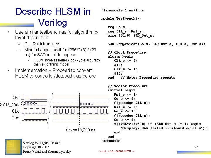
Describe HLSM in Verilog • `timescale 1 ns/1 ns module Testbench(); reg Go_s; reg Clk_s, Rst_s; wire [31: 0] SAD_Out_s; Use similar testbench as for algorithmiclevel description – Clk, Rst introduced – Minor change – wait for (256*2+3) * (20 ns) for SAD result to appear • • SAD Comp. To. Test(Go_s, SAD_Out_s, Clk_s, Rst_s); HLSM involves better clock cycle accuracy than algorithmic model Implementation – Proceed to convert HLSM to controller/datapath, as before Go SAD_Out Clk Rst time=10, 290 ns Verilog for Digital Design Copyright © 2007 Frank Vahid and Roman Lysecky // Clock Procedure always begin Clk_s <= 0; #10; Clk_s <= 1; #10; end // Note: Procedure repeats // Vector Procedure initial begin Rst_s <= 1; Go_s <= 0; @(posedge Clk_s); Rst_s <= 0; Go_s <= 1; @(posedge Clk_s); Go_s <= 0; #((256*2+3)*20) if ( SAD_Out_s != 4) begin $display("SAD failed -- should equal 4"); end endmodule vldd_ch 5_SADHLSMTB. v 36

Automated Synthesis from the Algorithmic Level • Behavioral synthesis (or high-level synthesis) tools – – Introduced in the 1990 s and 2000 s Automatically synthesize algorithmic-code to RTL code or directly to circuits Not yet adopted as widely as RTL synthesis tools Each tool imposes strong requirements and restrictions on the algorithmiclevel code – The quality of RTL code or circuits created from such tools also varies tremendously – Interesting direction and may prove increasingly useful in coming years Verilog for Digital Design Copyright © 2007 Frank Vahid and Roman Lysecky 37

Simulation Speed • Higher-level descriptions yield faster simulations – Due to fewer procedures, fewer variables, fewer events, . . . – 10 x difference means difference between tens of minutes versus hours; 100 x could mean days – High-level descriptions (e. g. , algorithmic) preferred early in design, and for integrated systems with many (hundreds) of sub-systems • One-procedure clocked procedure state machine is also faster than procedure approach where one procedure is combinational – Again, fewer procedures, fewer variables, fewer events, . . . • Differences become significant for very large systems, or for very lengthy testbenches Verilog for Digital Design Copyright © 2007 Frank Vahid and Roman Lysecky 38

Memory Verilog for Digital Design Copyright © 2007 Frank Vahid and Roman Lysecky 39

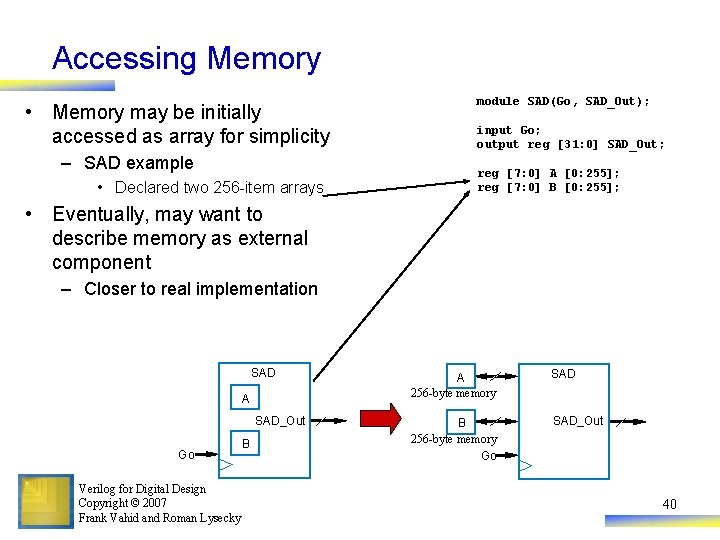
Accessing Memory • Memory may be initially accessed as array for simplicity – SAD example • Declared two 256 -item arrays module SAD(Go, SAD_Out); input Go; output reg [31: 0] SAD_Out; reg [7: 0] A [0: 255]; reg [7: 0] B [0: 255]; • Eventually, may want to describe memory as external component – Closer to real implementation SAD A 256 -byte memory SAD_Out B 256 -byte memory Go SAD_Out A Go Verilog for Digital Design Copyright © 2007 Frank Vahid and Roman Lysecky B 40

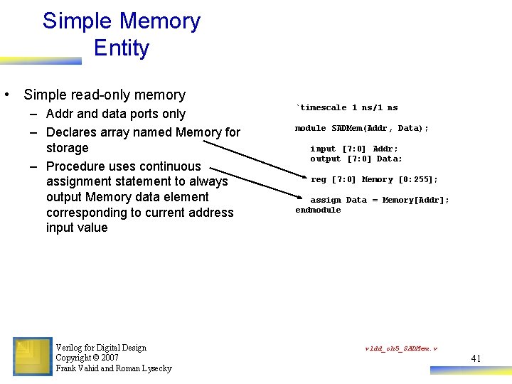
Simple Memory Entity • Simple read-only memory – Addr and data ports only – Declares array named Memory for storage – Procedure uses continuous assignment statement to always output Memory data element corresponding to current address input value Verilog for Digital Design Copyright © 2007 Frank Vahid and Roman Lysecky `timescale 1 ns/1 ns module SADMem(Addr, Data); input [7: 0] Addr; output [7: 0] Data; reg [7: 0] Memory [0: 255]; assign Data = Memory[Addr]; endmodule vldd_ch 5_SADMem. v 41

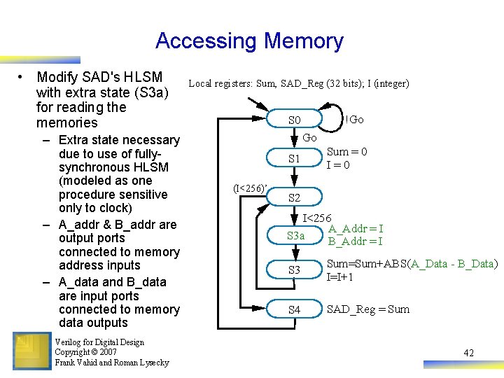
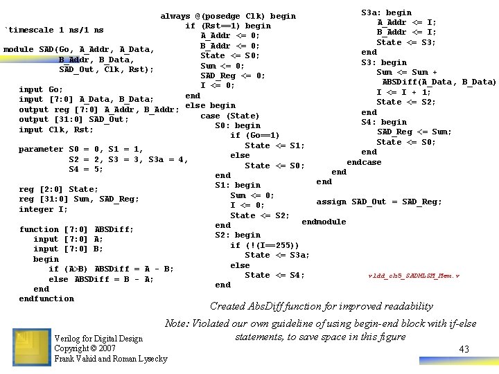
Accessing Memory • Modify SAD's HLSM with extra state (S 3 a) for reading the memories – Extra state necessary due to use of fullysynchronous HLSM (modeled as one procedure sensitive only to clock) – A_addr & B_addr are output ports connected to memory address inputs – A_data and B_data are input ports connected to memory data outputs Verilog for Digital Design Copyright © 2007 Frank Vahid and Roman Lysecky Local registers: Sum, SAD_Reg (32 bits); I (integer) !Go S 0 Go S 1 (I<256)’ Sum = 0 I=0 S 2 I<256 A_Addr = I S 3 a B_Addr = I S 3 Sum=Sum+ABS(A_Data - B_Data) I=I+1 S 4 SAD_Reg = Sum 42

S 3 a: begin always @(posedge Clk) begin A_Addr <= I; if (Rst==1) begin `timescale 1 ns/1 ns B_Addr <= I; A_Addr <= 0; State <= S 3; B_Addr <= 0; module SAD(Go, A_Addr, A_Data, end State <= S 0; B_Addr, B_Data, S 3: begin Sum <= 0; SAD_Out, Clk, Rst); Sum <= Sum + SAD_Reg <= 0; ABSDiff(A_Data, B_Data); I <= 0; input Go; I <= I + 1; end input [7: 0] A_Data, B_Data; State <= S 2; output reg [7: 0] A_Addr, B_Addr; else begin end case (State) output [31: 0] SAD_Out; S 4: begin S 0: begin input Clk, Rst; SAD_Reg <= Sum; if (Go==1) State <= S 0; State <= S 1; parameter S 0 = 0, S 1 = 1, end else S 2 = 2, S 3 = 3, S 3 a = 4, endcase State <= S 0; S 4 = 5; end end S 1: begin reg [2: 0] State; Sum <= 0; reg [31: 0] Sum, SAD_Reg; assign SAD_Out = SAD_Reg; I <= 0; integer I; State <= S 2; endmodule end function [7: 0] ABSDiff; S 2: begin input [7: 0] A; if (!(I==255)) input [7: 0] B; State <= S 3 a; begin else if (A>B) ABSDiff = A - B; State <= S 4; vldd_ch 5_SADHLSM_Mem. v else ABSDiff = B - A; end endfunction Created Abs. Diff function for improved readability Note: Violated our own guideline of using begin-end block with if-else statements, to save space in this figure Verilog for Digital Design Copyright © 2007 Frank Vahid and Roman Lysecky 43

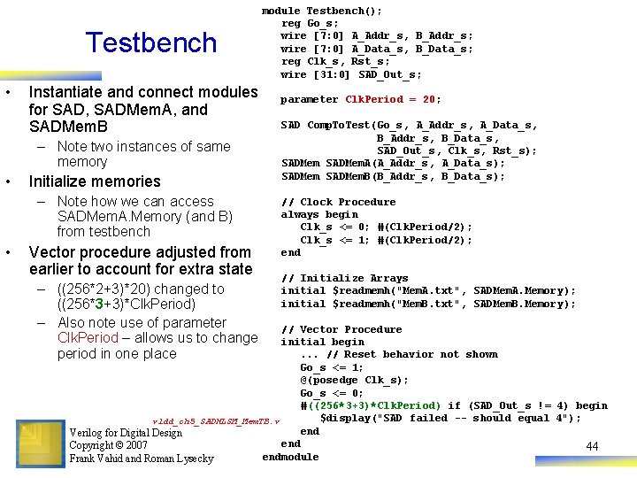
Testbench • Instantiate and connect modules for SAD, SADMem. A, and SADMem. B – Note two instances of same memory • Initialize memories – Note how we can access SADMem. A. Memory (and B) from testbench • Vector procedure adjusted from earlier to account for extra state – ((256*2+3)*20) changed to ((256*3+3)*Clk. Period) – Also note use of parameter Clk. Period – allows us to change period in one place module Testbench(); reg Go_s; wire [7: 0] A_Addr_s, B_Addr_s; wire [7: 0] A_Data_s, B_Data_s; reg Clk_s, Rst_s; wire [31: 0] SAD_Out_s; parameter Clk. Period = 20; SAD Comp. To. Test(Go_s, A_Addr_s, A_Data_s, B_Addr_s, B_Data_s, SAD_Out_s, Clk_s, Rst_s); SADMem. A(A_Addr_s, A_Data_s); SADMem. B(B_Addr_s, B_Data_s); // Clock Procedure always begin Clk_s <= 0; #(Clk. Period/2); Clk_s <= 1; #(Clk. Period/2); end // Initialize Arrays initial $readmemh("Mem. A. txt", SADMem. A. Memory); initial $readmemh("Mem. B. txt", SADMem. B. Memory); // Vector Procedure initial begin. . . // Reset behavior not shown Go_s <= 1; @(posedge Clk_s); Go_s <= 0; #((256*3+3)*Clk. Period) if (SAD_Out_s != 4) begin $display("SAD failed -- should equal 4"); vldd_ch 5_SADHLSM_Mem. TB. v end Verilog for Digital Design end Copyright © 2007 44 endmodule Frank Vahid and Roman Lysecky

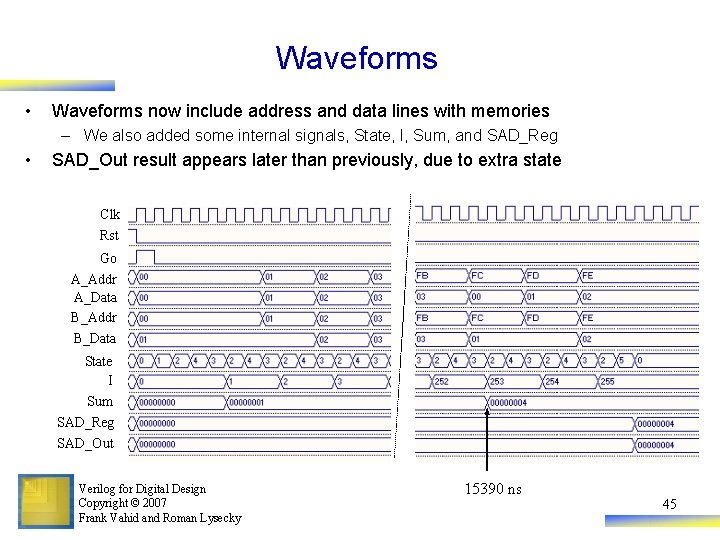
Waveforms • Waveforms now include address and data lines with memories – We also added some internal signals, State, I, Sum, and SAD_Reg • SAD_Out result appears later than previously, due to extra state Clk Rst Go A_Addr A_Data B_Addr B_Data State I Sum SAD_Reg SAD_Out Verilog for Digital Design Copyright © 2007 Frank Vahid and Roman Lysecky 15390 ns 45