Verilog A Cadence Inverter simulation tutorial 1 Continue
- Slides: 10

Verilog A - Cadence Inverter simulation tutorial 1

• Continue from “ 1_Loading_verilog. A_on_cadence. pptx” In the same way as you’ve included “NCNFET_L 1. va”, make a cell(symbol, verlioga) for “PCNFET_L 1. va” 2

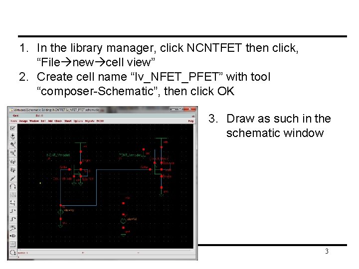
1. In the library manager, click NCNTFET then click, “File new cell view” 2. Create cell name “Iv_NFET_PFET” with tool “composer-Schematic”, then click OK 3. Draw as such in the schematic window 3

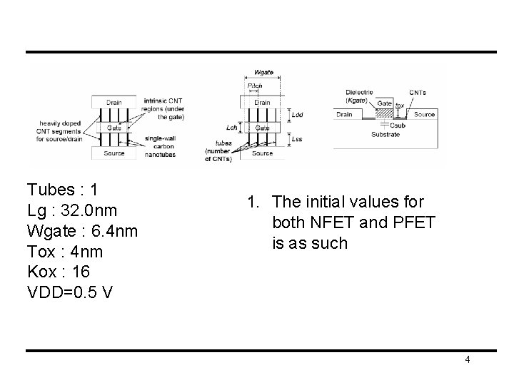
Tubes : 1 Lg : 32. 0 nm Wgate : 6. 4 nm Tox : 4 nm Kox : 16 VDD=0. 5 V 1. The initial values for both NFET and PFET is as such 4

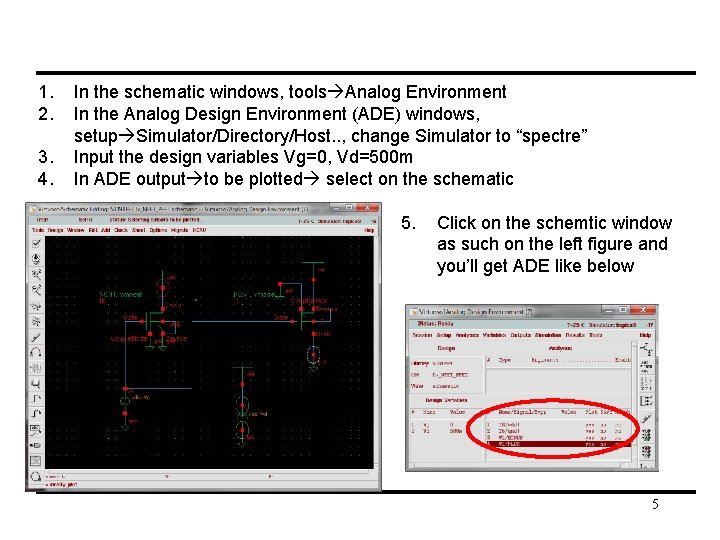
1. 2. 3. 4. In the schematic windows, tools Analog Environment In the Analog Design Environment (ADE) windows, setup Simulator/Directory/Host. . , change Simulator to “spectre” Input the design variables Vg=0, Vd=500 m In ADE output to be plotted select on the schematic 5. Click on the schemtic window as such on the left figure and you’ll get ADE like below 5

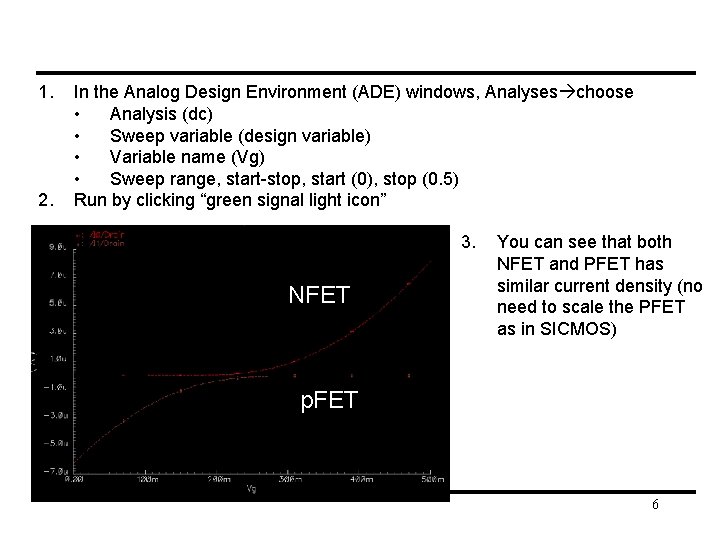
1. 2. In the Analog Design Environment (ADE) windows, Analyses choose • Analysis (dc) • Sweep variable (design variable) • Variable name (Vg) • Sweep range, start-stop, start (0), stop (0. 5) Run by clicking “green signal light icon” 3. NFET You can see that both NFET and PFET has similar current density (no need to scale the PFET as in SICMOS) p. FET 6

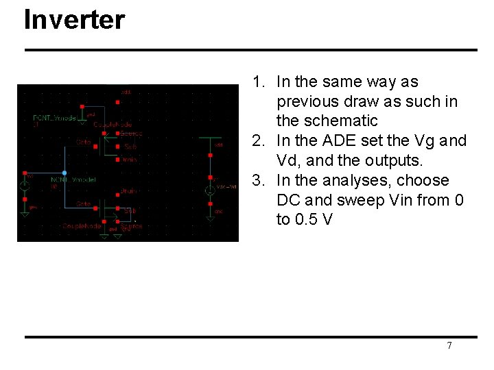
Inverter 1. In the same way as previous draw as such in the schematic 2. In the ADE set the Vg and Vd, and the outputs. 3. In the analyses, choose DC and sweep Vin from 0 to 0. 5 V 7

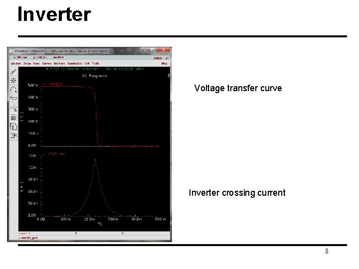
Inverter Voltage transfer curve Inverter crossing current 8

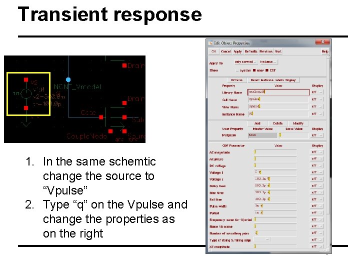
Transient response 1. In the same schemtic change the source to “Vpulse” 2. Type “q” on the Vpulse and change the properties as on the right 9

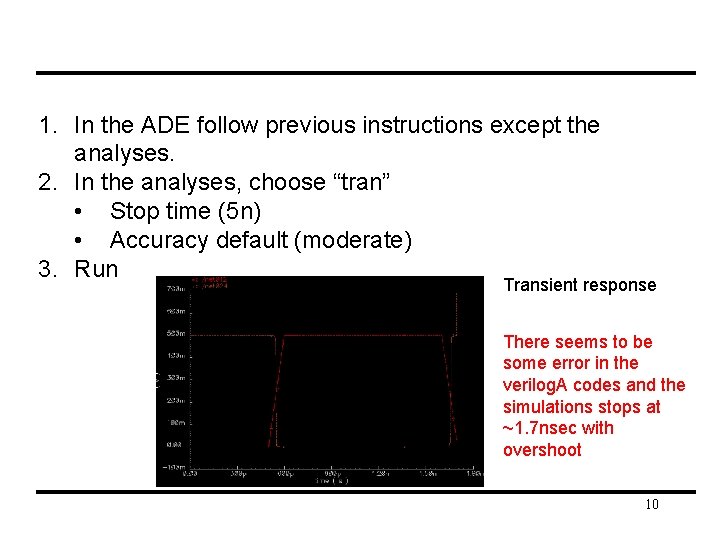
1. In the ADE follow previous instructions except the analyses. 2. In the analyses, choose “tran” • Stop time (5 n) • Accuracy default (moderate) 3. Run Transient response There seems to be some error in the verilog. A codes and the simulations stops at ~1. 7 nsec with overshoot 10