UW Madison Geoscience 777 Electron probe microanalysis Scanning

UW- Madison Geoscience 777 Electron probe microanalysis Scanning Electron Microscopy EPMA - SEM Acquiring Images in the SEM Modified 9/18/09 Modified 2/10/19

What’s the point? “A picture is worth a thousand words” The more we know about how images are acquired, the better we can present research results graphically. And we want to optimize the quality of our images, by understanding how various parameters affect the images.

Where do images come from? The sample responds to being bombarded by high energy (~15, 000) volts by generating many signals. . . Many which can be used to create images.

“SEM Imaging Modes”* You can distinguish 4 ‘end member’ types of SEM imaging: • High depth of field (mainly for 3 D images) • High spatial resolution • High current (for EBSD, EDS, mainly) • Low voltage By understanding what is different about how the SEM/column is optimized for each of these, you can improve your SEM images. You can also distinguish “high vacuum” from “variable pressure/low vacuum/environmental SEM. . . * From Goldstein et al, SEM & XRMA 4 th Edition 2018, Chapter 5. 3

Depth of Field for 3 D objects Light microscope image SEM SEI A strength of the SEM is the enhanced depth of field compared to optical microscopy as shown above for the radiolarian Trochodiscus longispinus. Optical image has only a few micron depth of field (=plane in focus), whereas SEM images can be made to be in focus for hundreds of microns by increasing the working distance Goldstein et al 2003 Fig 1. 3

Changing the depth of field W=working distance (mm between bottom of pole piece and sample surface To get greater depth of field of 3 D objects, (1) lower the stage, (2) possibly put in small aperture From Goldstein et al, SEM & XRMA 4 th Edition 2018, Chapter 5. 3
 resolution imaging • This means using secondary electrons (not BSEs) • Tighten")
High (spatial) resolution imaging • This means using secondary electrons (not BSEs) • Tighten the beam spot diameter: lower the current*, possibly higher k. V (next slide) • Reduce the working distance to minimum possible • Optimize the stigmation • If “in lens” SE detector available, use it to eliminate “scattered” secondary electrons * On some SEMs, there is a “spot size” knob--this really is NOT directly changing the “spot size”, rather it is changing the beam current which results in beam size From Goldstein et al, SEM & XRMA 4 th Edition 2018, Chapter 5. 3

Why do some say use high k. V for better images? A lot of books and folks with years of experience say that higher k. V gives better images. Goldstein For example, Goldstein et al 2003, p. 197 go thru an explanation why a 30 k. V image of Silicon would be sharp at 100, 000 X -- for a 1 nm! resolution beam on a 1024 x 1024 pixel image (=1 nm pixels) the 1 nm SE 1 “signal” would have a high signal/noise ratio, with the SE 2 noise “being constant” and therefore presumably vanishing. 2003 Fig. 5. 2 Figure caption: SE 1 has FWHM of 2 nm and SE 2 has FWHM of ~10 um. 30 ke. V probe, 1 nm beam, on silicon.

Why do some say use high k. V for better images? Nowhere in that text can I find an explanation why this is not the case also at say 15 k. V, and why 30 is better than 15 k. V. However, in the JEOL booklet, they say “theoretically the electron probe diameter is smaller”. My suggestion: be empirical… try going to higher, then to lower k. V, and see what you think is better…. And it may all be sample specific!
 resolution imaging • This means using secondary electrons (not BSEs) • Tighten")
High (spatial) resolution imaging • This means using secondary electrons (not BSEs) • Tighten the beam spot diameter: lower the current*, possibly higher k. V (next slide) • Reduce the working distance to minimum possible • Optimize the stigmation • If “in lens” SE detector available, use it to eliminate “scattered” secondary electrons * On some SEMs, there is a “spot size” knob--this really is NOT directly changing the “spot size”, rather it is changing the beam current which results in beam size From Goldstein et al, SEM & XRMA 4 th Edition 2018, Chapter 5. 3

SE 1 and SE 2 The picture gets a little more complicated … secondary electrons in fact can be generated and detected from more than just the “landing point” of the E 0 beam (SE 1’s). As the electron scatters away from the impact spot, if it stays near the surface, a second generation (SE 2’s) can be generated and detected -- these will cause the SE image to be less sharp. Solution: go to lower E 0 (5 k. V or less is mentioned by Goldstein) Goldstein et al 2003 Fig 3. 20

SE 1 and SE 2…and SE 3! And in the real world it may be even more complicated … backscattered electrons may bounce off the chamber walls, or the bottom of the column, generating SE 3’s. Because the E-T detector has a positive bias to attract the low energy SEs, these extraneous signals can add more noise to the image. This is especially problematic at high E 0 s and is a reason not to expect high resolution SE images at high k. V values. Goldstein et al 2003 Fig 4. 20
 can cause the beam")
Stigmatism Imperfect magnetic lenses (metal machining, electrical windings, dirty apertures) can cause the beam to be not exactly round, but “astigmatic”. This can be corrected using a “stigmator”, a set of 8 electromagnetic coils (bottom image). Top left: original “poor” image Top right: underfocus with stig Bottom left: overfocus with stig Bottom right: image corrected for astigmatism. Marker = 200 nm Goldstein et al 2003 Fig 2. 24

High current operation X-ray work EBSD work CL work • Secondary electron images are easy to acquire with rather low bream currents, say 100’s of p. A. • BSE images can also be acquired a lowish beam currents, however for maximum contrast of phases with similar BSE yields (=grey levels), higher beam currents may be needed (1 -10 or more n. A) • However, as X-rays are relatively rarer signals (vs SEs and BSEs), to achieve good precision, we need higher signal intensities, say 10’s to 100’s of n. A. • EBSD mapping at high spatial resolution also requires high beam currents, to allow fast processing of large area maps.

Low voltage imaging • Much less commonly used is “low voltage” imaging, meaning using something less than 15 k. V, usually 10 kv and below • This can be challenging, for many reasons, but also may be rewarding in providing a different view (sometimes “better”, sometimes “worse”) of the sample • Key is the fact that the electron scattering range is reduced, sometimes significantly • This decrease goes approximately as a 1. 7 power, i. e. dropping from 15 to 1. 5 k. V will reduce the electron range (scatter) by 101. 7 -- a factor of 50!
, you")
Low voltage imaging • At very low voltages (a couple of k. V), you do not need to coat your sample! • Also at low voltages, there is potentially less damage to fragile (e. g. biological) samples (assuming you are using very low beam currents); though this needs to be determined empirically

Goldstein et al 2003 Figure 5. 1 As seen in the figure SE 1’s (and BSE 1’s) occur immediately at the beam impact point. Of course, electrons continue to scatter within the sample and SE 2’s (and BSE 2’s) will emerge over a range of distances from that central point. Dropping the E 0 therefore might produce better resolution electron images. However there are issues to understand:

There are potentially limits, however, to low voltage imaging: • Will the gun put out a “bright” (strong, tight) enough beam at the particular lower voltage? • Is the sample surface clean? Going to lower k. V means that any stuff (fingerprints, hydrocarbons, dust) on the surface will be preferentially enhanced in the image. -- On the other hand, if what you WANT to image is the surface, lower k. V is definitely called for! • SE detectors operate pretty well down to very low voltages (at or below 1 k. V). • However, many BSE detectors start to become less sensitive as you drop below 10 k. V. However, our Hitachi S 3400 BSE detector works very well below 5 k. V and even gives a weak image at 1 k. V.
 SEM: Need Conductivity! Above left: uncoated. A charge builds up causes")
High Vacuum (traditional) SEM: Need Conductivity! Above left: uncoated. A charge builds up causes oversaturation (white) and horizontal streaking from beam Above right: what same area would appear with conductive coating Right: High vacuum carbon coater (“evaporator” not sputterer). This is the old original version with oil diffusion pump (now replaced with turbo pump).

Edge Effects Edges of objects can appear to be brighter in SE and BSE images, because electrons can be emitted not only from the top but the side, artifically making that part of the image brighter. This can lead to some incorrect conclusions for BSE images. Note: this explanation is for topography. Reed 2005 Fig 4. 3

Secondary electron images SE imaging: the signal is from the top 5 nm in metals, and the top 50 nm in insulators. Thus, fine scale surface features are imaged. The detector is located to one side, so there is a shadow effect – one side is brighter than the opposite. Everhart-Thornley detector: low-energy secondary electrons are attracted by +200 V on grid and accelerated onto scintillator by +10 k. V bias; light produced by scintillator (phosphor surface) passes along light pipe to external photomultiplier (PM) which converts light to electric signal. Back scattered electrons also detected but less efficiently because they have higher energy and are not significantly deflected by grid potential. (image and text from Reed, 1996, p. 37)

BSE images There are several different types of detectors used to acquire BSE images: (1) Everhart-Thornley detector can have a 50 e. V bias put on the grid to reject secondary electrons, so only BSEs get thru -- however this is not useful at fast, TV scanning rates, i. e. moving the stage. BSE imaging: the signal comes from the top ~. 1 um surface). Above, 5 phases stand out in a volcanic ash fragment (2) Robinson detector — a modern version of the E-T for BSE at TV rates. Must be inserted and retracted. (3) Solid state detector — which is most commonly used today on electron microprobes and many SEMs. Permanently mounted below pole piece.

BSE images BSE imaging: the signal comes from the top ~. 1 um surface; solid-state detector is sensitive to light (and red LEDs). A solid-state (semi-conductor) backscattered electron detector (a) is energized by incident high energy electrons (~90% E 0), wherein electron-hole pairs are generated and swept to opposite poles by an applied bias voltage. This charge is collected and input into an amplifier (gain of ~1000). (b) It is positioned directly above the specimen, surrounding the opening through the polepiece. You are able to modify the amplifier gain by switching between different levels. Goldstein et al, 1992, Fig 4. 24, p. 184

Variations on a theme There are several alternative type SEM images sometimes found in BSE or SE imaging: (left) channeling (BSE) and (right) magnetic contrast (SE). I have found BSE images of single phase metals with crystalline structure shown by the first effect, and suspect the second effect may be the cause of problems with some Mn. Ni phases. Crystal lattice shown above, with 2 beam-crystal orientations: (a) nonchanneling, and (b) channelling. Less BS electrons get out in B, so darker. From Newbury et al, 1986, Advanced Scanning Electron Microscopy and X-ray Microanalysis, Plenum, p. 88 and 159.

BSE and SE Detectors on our CAMECA SX 51 EPMA Anticontamination air jet Annular BSE detectors Plates for +voltage for SE detector View from inside, looking up obliquely (image taken by handheld digital camera)

Hitachi SEM Detectors Annular BSE detector EDS detector ESED detector E-T SE detector View from inside, looking up obliquely (image taken by handheld digital camera) IR Chamber scope

Images: • Optimal adjustment of brightness and contrast critical for BSE of samples with different phases/chemistries • Sharpness of images resolution • Field of view how to increase • Documentation Scale bars

BSE Brightness/Contrast Example 1 Washed out whites

BSE Brightness/Contrast Example 1 Turn down brightness, turn up contrast!

BSE Brightness/Contrast Example 1 Ti-magnetite Ilmenite Critical mineral pair would have not been found! Fe-Ti oxide pair are an important geothermometer and oxygen fugacity indicator

BSE Brightness/Contrast Example 2 Washed out whites

BSE Brightness/Contrast Example 2 Pyrite Ilmenite Strange partners?

BSE Brightness/Contrast Example 3 Washed out whites

BSE Brightness/Contrast Example 3 Apatite inside Ti-magnetite

Sharpness = Focusing Image Resolution • Start with SE image • Coarse focus at low magnification • Zoom to highest magnification possible and fine focus • Stigmate (twist both knobs one at a time, fine “average good” for each) • Switch to BSE if that is mode desired

SEM Resolution However, the approach apparently used today (e. g. our Hitachi field service engineer) is to take his “test sample” (gold sputtered on graphite substrate) and with optimized contrast, find the narrowest spacing between 2 gold blobs and define that as the “resolution”.

SEM Resolution The above 2 scans show the technique (though apparently the proofreader didn’t catch the inverted signal on the left image). The only way to increase resolution is to turn DOWN the beam current, as the plot on the right shows dramatically -the current is a few tens of picoamps, not nanoamps. Lyman et al, 1990, “Lehigh Lab Workbook”, Figs A 2. 3, A 2. 4, p. 191

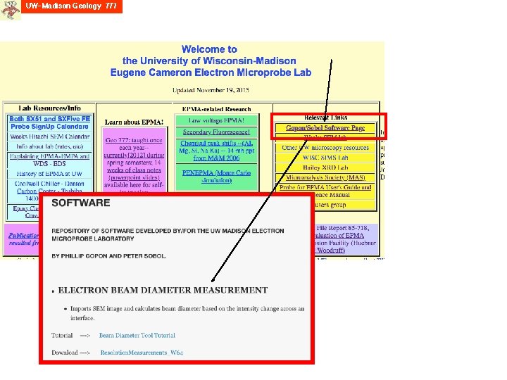
SEM Resolution: K 409 We found a “failed” NIST-standard that makes a great resolution standard for FE-microprobes. Peter Sobol wrote a program that automatically calculates the beam resolution.

From “A Guide to Scanning Microscope Observation” by JEOL “When theoretically considering the electron probe diameter alone, the higher the accelerating voltage, the smaller the electron probe [at constant electron flux]. However, there are some unnegligible demerits in increasing the accelerating voltage. They are mainly as follows: 1. Lack of detailed structures of specimen surfaces 2. Remarkable edge effect 3. Higher possibility of charge-up 4. Higher possibility of specimen damage. ” This suggests to me: if you want to “pass a test” with Au-spheres on graphite, 30 k. V is better…. but for “real” samples, maybe lower k. V will produce a better image…

Wider Field of View: Move the sample down or Make a mosaic/tiled image

Mosaic Images There are occasions where the feature you wish to image is larger than the field of view acquirable by the rastered beam. A complete thin section (24 x 48 mm) can have a mosaic BSE image acquired in < 1 hour (though an Xray map could take a week, so only smaller areas are typically X-ray mapped. ) This is achieved by tiling or mosaicing smaller images together. The software calculates how many smaller images are needed based upon the field of view at the magnification used, drives to the center of each rectangle, and then seemlessly stitches the images into one whole. The false colored BSE image of a cm-sized zoned garnet to the right was made by many (>100) 63 x scans (each scan 1. 9 mm max width). From research of Cory Clechenko and John Valley.
 frames ICE program: Image")
ICE is NICE! Zircon CL image: 70 (10 x 7) frames ICE program: Image Composite Editor <www. microsoft. com/en-us/research/product/computationalphotography-applications/image-composite-editor>

Image Documentation: Scale bars, LUT • Always include a scale bar in all images, with numbers/words easily readable • Always include a LUT (look up table) if using colors for distinguishing intensity values Without a scale bar and LUT, you’d have no idea of the size nor whether green was higher or lower Ca than orange

Image Documentation: Scale bars, LUT • Always include a scale bar in all images, with numbers/words easily readable • Always include a LUT (look up table) if using colors for distinguishing intensity values • Always state explicitly what kind of signal (SE, BSE, CL, ESED, Absorbed current, X-ray line) • If X-ray map, always state if background substracted (essential for older systems) • Always include somewhat a description of the conditions (minimally the instrument and the k. V)

Suggested references “A Guide to Scanning Microscope Observation” by JEOL <http: //www. geology. wisc. edu/~johnf/g 777/JEOLguide. pdf> and “Invitation to the SEM World” by JEOL <http: //www. geology. wisc. edu/~johnf/g 777/Invitation. SEM. pdf> Also many others are available on line as well from JEOL: https: //www. jeolusa. com/RESOURCES/Electron. Optics/Documents-Downloads
- Slides: 46