UVCurved Nano Imprint Lithography Lithography ImprintTo produce a

- Slides: 18

UV-Curved Nano Imprint Lithography

�Lithography �Imprint-To produce (a mark or pattern) on a surface by pressure. �Nanoscale �Uv- Method

Introduction �This was first invented by Prof. Stephen Chou and his students in 1995. �This is a method of fabricating nanometer scale patterns. �It creates patterns by mechanical deformation of imprint resist and subsequent processes. �This is the road map for the 32 -nm semiconductor technology

Requirements �The materials required for the Imprint technique is �(i) a mold with predefined surface relief nanostructures, and �(ii) a suitable resist material that can be deformed and hardened to preserve the shape of the impression.

Mold Fabrication �Thermal expansion co-efficient is an important factor to be considered. �Si, Si. O 2, Si. C, silicon nitride, metals, sapphire, and diamond film.

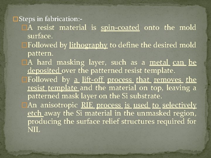
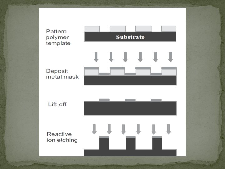
� Steps in fabrication: - �A resist material is spin-coated onto the mold surface. �Followed by lithography to define the desired mold pattern. �A hard masking layer, such as a metal can be deposited over the patterned resist template. �Followed by a lift-off process that removes the resist template and the material on top, leaving a patterned mask layer on the Si substrate. �An anisotropic RIE process is used to selectively etch away the Si material in the unmasked region, producing the surface relief structures required for NIL


Types � Thermoplastic Nanoimprint lithography � Uv-curved Nano. Imprint Lithographhy � Roll imprint process, � Laser-assisted direct imprint, � Reverse imprint lithography, � Substrate conformal imprint lithography, � Ultrasonic NIL, etc.

Uv-Curved Method � The UV curved Nanoimprint Lithography is normally carried out in room temperature and at low pressure. � The mold material used is of transparent type fused with silica. � Here we do use the soft UV for the lithographic process. � The resist material used is the liquid polymer but in thermal method they use thermal plastic.

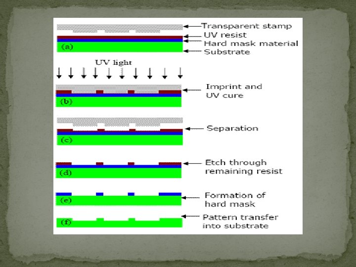
Principle: �The transparent mold is pressed over the resist material. �Now the cavities are fully filled by the resist. �Now the resist is curved by the UV-rays so that the resist will become solid and it is etched till the base. �After demolding, a similar pattern transfer process can be used to transfer the pattern in resist onto the underneath material


Crucial process issues for NIL �Thickness and uniformity of residual layer. . �Pattern fidelity(Precision) �Defect control �Filling process

Key concern for NIL templates �Template surface treatment �Defect inspection. �Lifetime.

Advantages � Nanoimprint lithography has experimentally been shown to achieve 25 nm feature size. � The promise of repeatability and durability consequently leads this to low costs and ease of fabrication.

Draw. Backs � The surface sticking problem has not been perfected. � The molding conditions haven’t been optimized. � The effect of thermal expansion through the process is not fully understood.

Applications � Nanoimprint lithography has been used to fabricate devices for electrical, optical, photonic and biological application. � For electronics devices, NIL has been used to fabricate MOSFET, O-TFT, single electron memory. For optics and photonics, intensive study has been conducted in fabrication of subwavelength resonant grating filter, polarizers, waveplate, anti-reflective structures, integrated photonics circuit and plasmontic devices by NIL.

The future of nanoimprint �Nanoimprint lithography is a simple pattern transfer process that is neither limited by diffraction nor scattering effects nor secondary electrons, and does not require any sophisticated radiation chemistry. It is also a potentially simple and inexpensive technique. �However, a lingering barrier to nanometer-scale patterning is the current reliance on other lithography techniques to generate the template. �As of October 2007, Toshiba is the only company to have validated nanoimprint lithography for 22 nm and beyond.

Reference �S. Chou, P. Krauss, P. Renstrom, 1996, “Nanoimprint lithography, ” J. Vac. Sci. Technol. B, Volume 14(6), pp. 4129 -4133. �S. Chou, P. Krauss, P. Renstrom, 1996, “Imprint Lithography with 25 -Nanometer Resolution, ” SCIENCE, Volume 272, pp. 85 -87. �www. wikipedeia. org