Using Virtual Platforms for Firmware Verification James Pangburn

Using Virtual Platforms for Firmware Verification James Pangburn Jason Andrews
About the Authors § James Pangburn − (Cadence, jpangburn@cadence. com, 408 -914 -6386) − Firmware Architect at Cadence, 30 years experience in hardware and software development, embedded systems, EDA tools § Jason Andrews − (Cadence, jasona@cadence. com, 763 -862 -1655) − Senior Architect at Cadence, responsible for embedded software and hardware/software coverification products and methodology 2 © 2013 Cadence Design Systems, Inc. All rights reserved.
Agenda • Problem Statement • Solution: Virtual Platforms – How to build them – How they help firmware verification • Tested Examples • Conclusion 4 © 2013 Cadence Design Systems, Inc. All rights reserved.
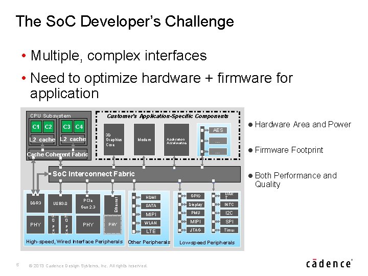
The So. C Developer’s Challenge • Multiple, complex interfaces • Need to optimize hardware + firmware for application CPU Subsystem Customer’s Application-Specific Components C 3 C 4 C 1 C 2 L 2 cache 3 D Graphics Core AES Modem Application Accelerators … PHY USB 3. 0 2. 0 P H Y Gen 2, 3 PHY Ethernet So. C Interconnect Fabric DDR 3 PHY l Firmware Footprint l Both Performance and Quality HDMI GPIO UAR T SATA Display INTC MIPI PMU I 2 C WLAN LTE High-speed, Wired Interface Peripherals Other Peripherals 5 Area and Power … Cache Coherent Fabric PCIe l Hardware © 2013 Cadence Design Systems, Inc. All rights reserved. MIPI SPI Low-speed peripheral JTAG Timer subsystem Low-speed Peripherals
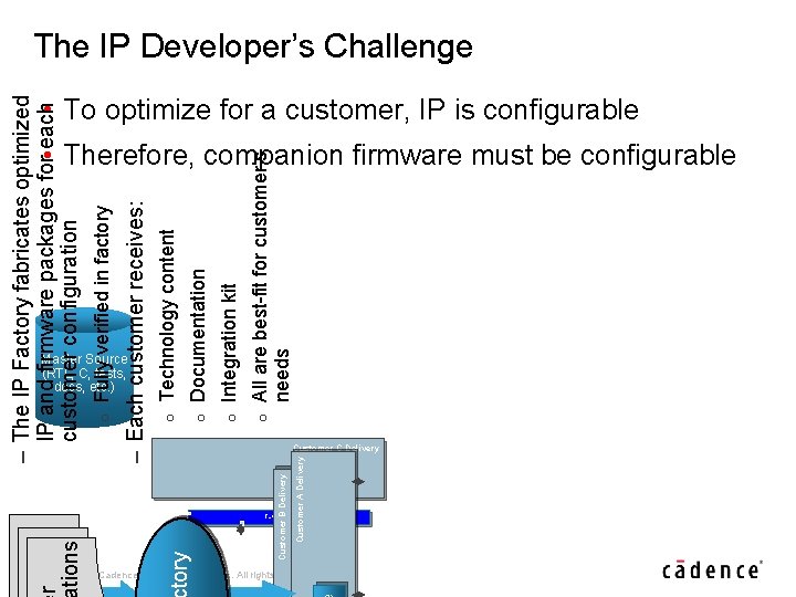
© 2013 Cadence Design Systems, Inc. All rights reserved. Other JTAG er GPIO Modem Other Peripherals o Fully verified in factory Technology content Documentation Integration kit All are best-fit for customer’s needs o o o • Therefore, companion firmware must be configurable o – Each customer receives: Customer A Delivery Other Customer B Delivery C JTAG Other GPIO TLM Router RT 6 tions Master Source (RTL, C, tests, docs, etc. ) tory r – The IP Factory fabricates optimized IP and firmware packages for each customer configuration The IP Developer’s Challenge • To optimize for a customer, IP is configurable Customer C Delivery
The Problem at Hand • How to verify that the generated firmware is correct? − Drives the selected configuration of the IP − Causes the IP to perform the functions as understood by the firmware developers • Catch errors, misunderstandings, etc. early 7 © 2013 Cadence Design Systems, Inc. All rights reserved.
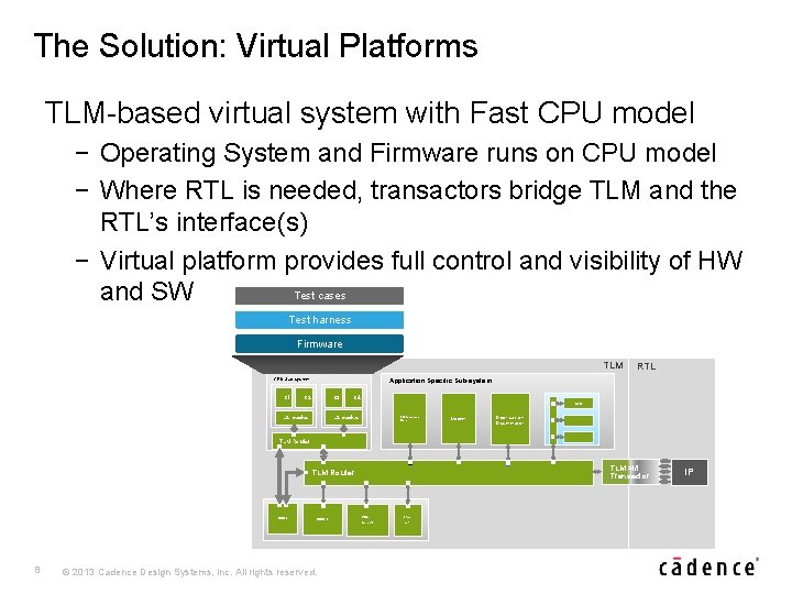
The Solution: Virtual Platforms TLM-based virtual system with Fast CPU model − Operating System and Firmware runs on CPU model − Where RTL is needed, transactors bridge TLM and the RTL’s interface(s) − Virtual platform provides full control and visibility of HW Test cases and SW Test harness Firmware TLM CPU Sub-system C 1 RTL Application Specific Sub-system C 3 C 2 C 4 AES L 2 cache 3 D Graphics Core … TLM >i/f Transactor TLM Router 8 Application Accelerator … TLM Router DDR 3 Modem USB 3. 0 © 2013 Cadence Design Systems, Inc. All rights reserved. PCIe Ether Gen 2, 3 net IP
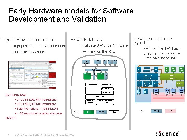
Early Hardware models for Software Development and Validation VP platform available before RTL VP with RTL Hybrid • High performance SW execution • Validate SW driver/firmware • Run entire SW stack • Running on the RTL GIC SRAM Arm Processor VP with Palladium® XP Hybrid • Run entire SW Stack • On RTL in Palladium for majority of So. C Timer UART Term TLM Wrapper Host PCIe Core Drv Mouse CDDC USB Linux Shell Cmds Unit Test Func SMP Linux boot: UDR kernel Module • CPU 1 489, 558, 519 instructions • In 30 seconds on a laptop computer Key: 36 MIPS 9 © 2013 Cadence Design Systems, Inc. All rights reserved. RTL NV NV Flow Clock Timer Control MUX (c. Router) c. Router (subsyst. cfg) (top. cfg) Frame Real Buffer Time Mon Clock UI VNC_ SDL Loader Fast Model reset Smart AXI Interrupt Manager Mem Bridge Manager So. C PCIe RC Initialization Module TLM SW Key: interrupt Reset Linux Kernel • CPU 0 615, 093, 547 instructions • Total Instructions: 1, 104, 652, 066 Keyboard PCIe Core Register Access UART Socket Serv SRAM PIPE 3 PCIe Core e. MMC TLM RTL
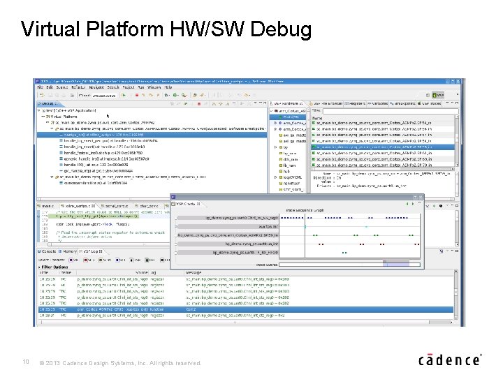
Virtual Platform HW/SW Debug 10 © 2013 Cadence Design Systems, Inc. All rights reserved.
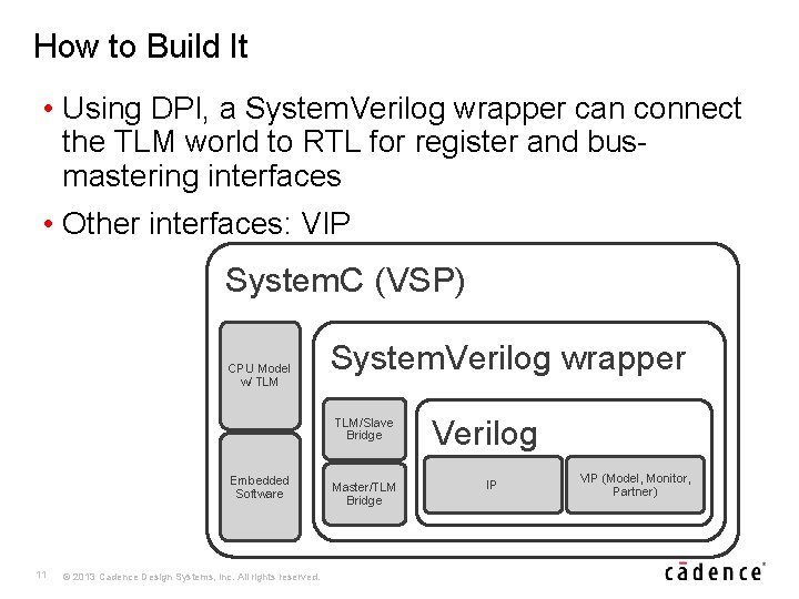
How to Build It • Using DPI, a System. Verilog wrapper can connect the TLM world to RTL for register and busmastering interfaces • Other interfaces: VIP System. C (VSP) CPU Model w/ TLM System. Verilog wrapper TLM/Slave Bridge Embedded Software 11 © 2013 Cadence Design Systems, Inc. All rights reserved. Master/TLM Bridge Verilog IP VIP (Model, Monitor, Partner)
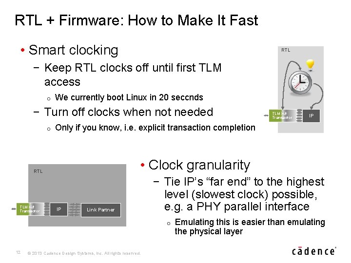
RTL + Firmware: How to Make It Fast • Smart clocking RTL − Keep RTL clocks off until first TLM access o We currently boot Linux in 20 seccnds − Turn off clocks when not needed o • Clock granularity IP Link Partner − Tie IP’s “far end” to the highest level (slowest clock) possible, e. g. a PHY parallel interface o 12 IP Only if you know, i. e. explicit transaction completion RTL TLM >i/f Transactor © 2013 Cadence Design Systems, Inc. All rights reserved. Emulating this is easier than emulating the physical layer
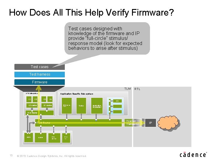
How Does All This Help Verify Firmware? Test cases designed with knowledge of the firmware and IP provide “full-circle” stimulus/ response model (look for expected behaviors to arise after stimulus) Test cases Test harness Firmware TLM CPU Sub-system C 1 RTL Application Specific Sub-system C 3 C 2 C 4 AES L 2 cache 3 D Graphics Core Modem TLM >i/f Transactor TLM Router 13 … … TLM Router DDR 3 Application Accelerator USB 3. 0 PCIe Ether Gen 2, 3 net © 2013 Cadence Design Systems, Inc. All rights reserved. IP
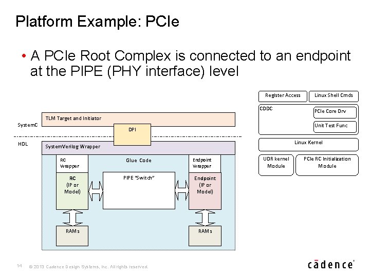
Platform Example: PCIe • A PCIe Root Complex is connected to an endpoint at the PIPE (PHY interface) level Register Access CDDC System. C HDL PCIe Core Drv TLM Target and Initiator Unit Test Func DPI Linux Kernel System. Verilog Wrapper RC (IP or Model) Glue Code PIPE “Switch” RAMs 14 Linux Shell Cmds © 2013 Cadence Design Systems, Inc. All rights reserved. Endpoint Wrapper Endpoint (IP or Model) RAMs UDR kernel Module PCIe RC Initialization Module
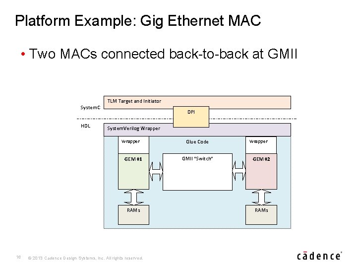
Platform Example: Gig Ethernet MAC • Two MACs connected back-to-back at GMII System. C HDL TLM Target and Initiator DPI System. Verilog Wrapper GEM #1 RAMs 16 © 2013 Cadence Design Systems, Inc. All rights reserved. Glue Code GMII “Switch” Wrapper GEM #2 RAMs
Conclusion: Time Saved • Physical hardware platform creation − Avoid all issues with boards: acquiring, board-specific IP builds and glue code, bring up • Firmware development − Need not wait for hardware bring up/stability • Firmware verification − 17 Can exercise all code due to ease of error injection (through virtual registers, test harness can inject faults in “switches” or VIP models) © 2013 Cadence Design Systems, Inc. All rights reserved.
- Slides: 15