Using Module Compiler to build FPGA Structures st
Using Module Compiler to build FPGA Structures st Robu Low Robust er Pow LSI V Power VLSI Seyi Ayorinde ECE 6505
Outline § Architectures § § FPGA Look-Up Table (LUT) Configurable Logic Block (CLB) Switch Box § Using Module Compiler § Approach § Challenges st Robu Low er Pow VLSI 2
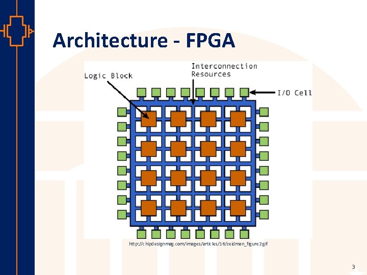
Architecture - FPGA st Robu Low er Pow VLSI http: //chipdesignmag. com/images/articles/16/zeidman_figure 2. gif 3
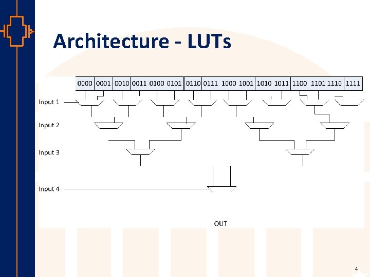
Architecture - LUTs st Robu Low er Pow VLSI 4
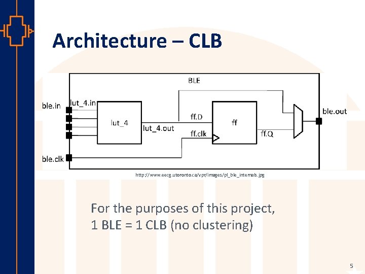
Architecture – CLB http: //www. eecg. utoronto. ca/vpr/images/pl_ble_internals. jpg st Robu Low er Pow VLSI For the purposes of this project, 1 BLE = 1 CLB (no clustering) 5
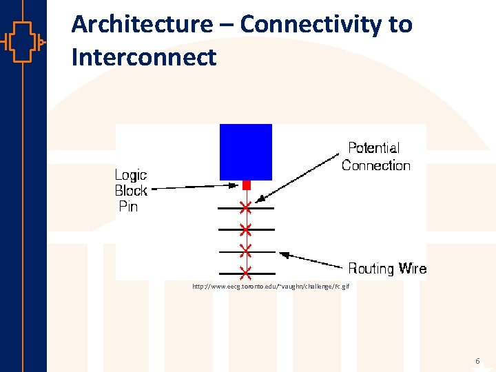
Architecture – Connectivity to Interconnect st Robu Low er Pow VLSI http: //www. eecg. toronto. edu/~vaughn/challenge/Fc. gif 6
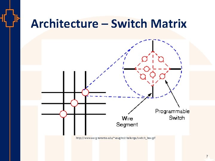
Architecture – Switch Matrix st Robu Low er Pow VLSI http: //www. eecg. toronto. edu/~vaughn/challenge/switch_box. gif 7
Project Architecture § 100 CLBs § 10 x 10 Array § 4 -Input LUTs § No Clustering § Channel Width – 4 st Robu Low er Pow VLSI § Reconfigurable Switch – Mux 8
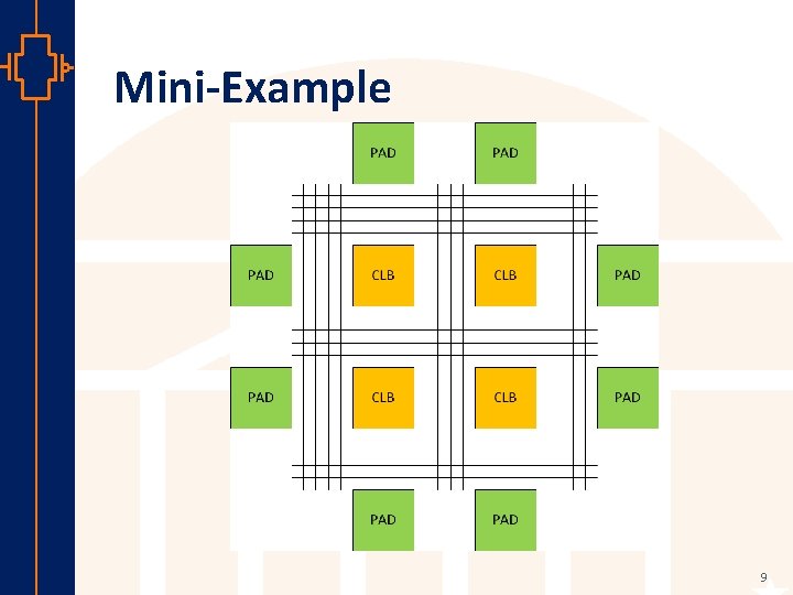
Mini-Example st Robu Low er Pow VLSI 9
Approach § Module Compiler – Relative Placement § Places portions of the design in specific areas relative to each other § Uses a grid of rows and columns § (0, 0) is bottom left corner st Robu Low er Pow VLSI 10
Acronyms § HC and VC – Horizontal and Vertical Channels § SM – Switch Matrix § CLB – Configurable Logic Block st Robu Low er Pow VLSI 11
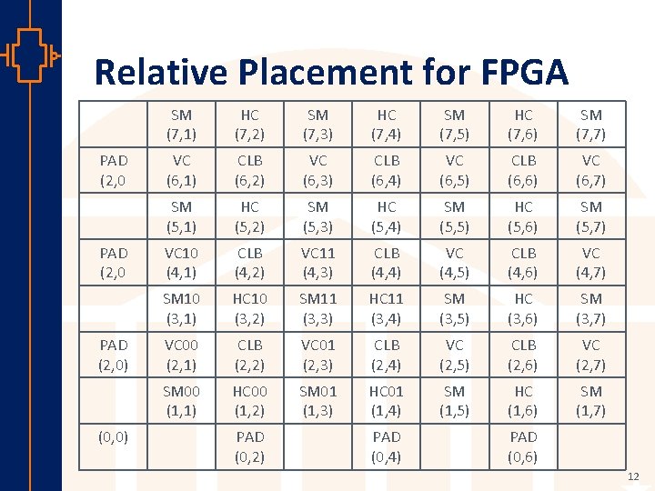
Relative Placement for FPGA PAD (2, 0) st Robu Low er Pow VLSI (0, 0) SM (7, 1) HC (7, 2) SM (7, 3) HC (7, 4) SM (7, 5) HC (7, 6) SM (7, 7) VC (6, 1) CLB (6, 2) VC (6, 3) CLB (6, 4) VC (6, 5) CLB (6, 6) VC (6, 7) SM (5, 1) HC (5, 2) SM (5, 3) HC (5, 4) SM (5, 5) HC (5, 6) SM (5, 7) VC 10 (4, 1) CLB (4, 2) VC 11 (4, 3) CLB (4, 4) VC (4, 5) CLB (4, 6) VC (4, 7) SM 10 (3, 1) HC 10 (3, 2) SM 11 (3, 3) HC 11 (3, 4) SM (3, 5) HC (3, 6) SM (3, 7) VC 00 (2, 1) CLB (2, 2) VC 01 (2, 3) CLB (2, 4) VC (2, 5) CLB (2, 6) VC (2, 7) SM 00 (1, 1) HC 00 (1, 2) SM 01 (1, 3) HC 01 (1, 4) SM (1, 5) HC (1, 6) SM (1, 7) PAD (0, 2) PAD (0, 4) PAD (0, 6) 12
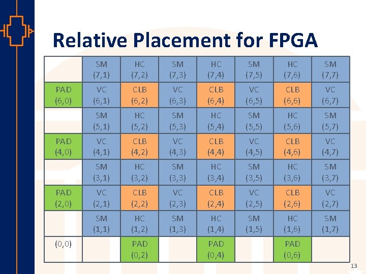
Relative Placement for FPGA PAD (6, 0) PAD (4, 0) PAD (2, 0) st Robu Low er Pow VLSI (0, 0) SM (7, 1) HC (7, 2) SM (7, 3) HC (7, 4) SM (7, 5) HC (7, 6) SM (7, 7) VC (6, 1) CLB (6, 2) VC (6, 3) CLB (6, 4) VC (6, 5) CLB (6, 6) VC (6, 7) SM (5, 1) HC (5, 2) SM (5, 3) HC (5, 4) SM (5, 5) HC (5, 6) SM (5, 7) VC (4, 1) CLB (4, 2) VC (4, 3) CLB (4, 4) VC (4, 5) CLB (4, 6) VC (4, 7) SM (3, 1) HC (3, 2) SM (3, 3) HC (3, 4) SM (3, 5) HC (3, 6) SM (3, 7) VC (2, 1) CLB (2, 2) VC (2, 3) CLB (2, 4) VC (2, 5) CLB (2, 6) VC (2, 7) SM (1, 1) HC (1, 2) SM (1, 3) HC (1, 4) SM (1, 5) HC (1, 6) SM (1, 7) PAD (0, 2) PAD (0, 4) PAD (0, 6) 13
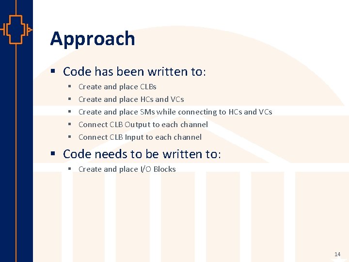
Approach § Code has been written to: § § § Create and place CLBs Create and place HCs and VCs Create and place SMs while connecting to HCs and VCs Connect CLB Output to each channel Connect CLB Input to each channel § Code needs to be written to: § Create and place I/O Blocks st Robu Low er Pow VLSI 14
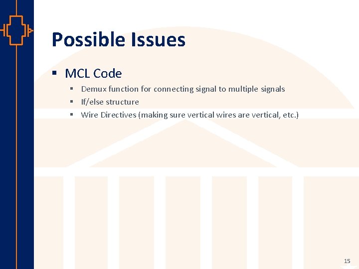
Possible Issues § MCL Code § Demux function for connecting signal to multiple signals § If/else structure § Wire Directives (making sure vertical wires are vertical, etc. ) st Robu Low er Pow VLSI 15
(Immediate) Future Work § Add I/O Blocks § Debug Code st Robu Low er Pow VLSI 16
Deliverables § MCL Code § Other MC Outputs § Layout file, Report Files, etc. § VHDL Code (Output of Module Compiler) § Schematic View § Layout (? ) st Robu Low er Pow VLSI § Analysis of MC 17
Questions? st Robu Low er Pow VLSI 18
- Slides: 18