
Using Direct Memory Access to Improve Performance ARM
- Slides: 18
Using Direct Memory Access to Improve Performance ARM University Program Copyright © ARM Ltd 2013 1
Overview § Basic Concepts § DMA Peripherals in Cortex-M 0+ § DMA Applications § § Data Transfer Replacing ISRs ARM University Program Copyright © ARM Ltd 2013 2
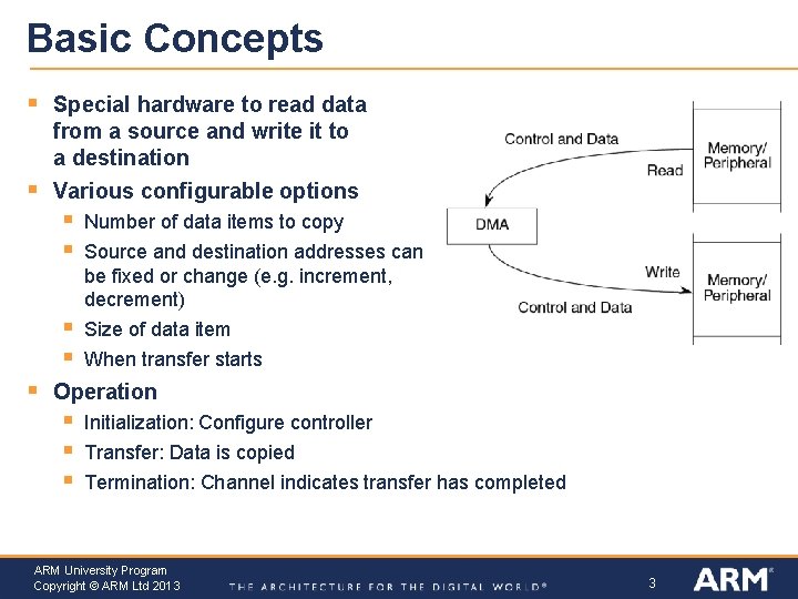
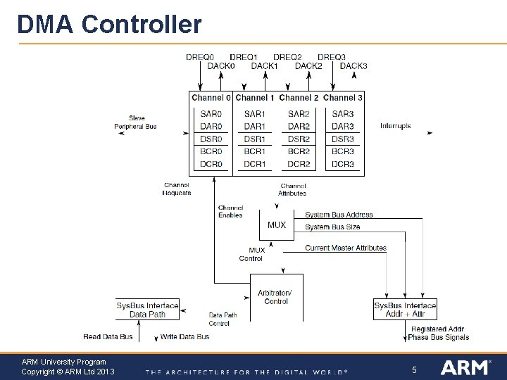
Basic Concepts § § Special hardware to read data from a source and write it to a destination Various configurable options § § § Number of data items to copy Source and destination addresses can be fixed or change (e. g. increment, decrement) Size of data item When transfer starts Operation § § § Initialization: Configure controller Transfer: Data is copied Termination: Channel indicates transfer has completed ARM University Program Copyright © ARM Ltd 2013 3
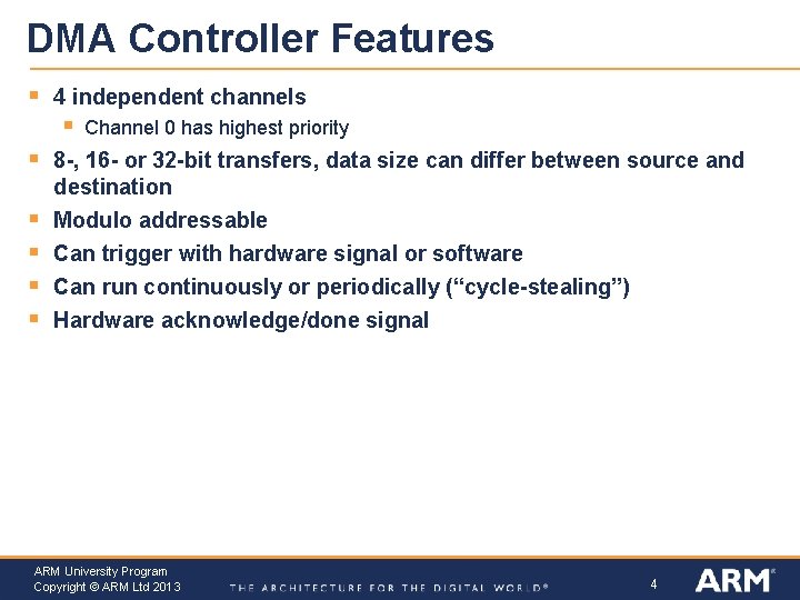
DMA Controller Features § 4 independent channels § § § Channel 0 has highest priority 8 -, 16 - or 32 -bit transfers, data size can differ between source and destination Modulo addressable Can trigger with hardware signal or software Can run continuously or periodically (“cycle-stealing”) Hardware acknowledge/done signal ARM University Program Copyright © ARM Ltd 2013 4
DMA Controller ARM University Program Copyright © ARM Ltd 2013 5
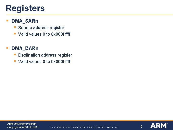
Registers § DMA_SARn § § § Source address register, Valid values 0 to 0 x 000 f ffff DMA_DARn § § Destination address register Valid values 0 to 0 x 000 f ffff ARM University Program Copyright © ARM Ltd 2013 6
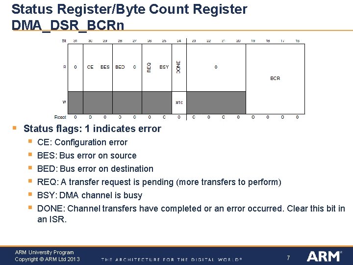
Status Register/Byte Count Register DMA_DSR_BCRn § Status flags: 1 indicates error § § § CE: Configuration error BES: Bus error on source BED: Bus error on destination REQ: A transfer request is pending (more transfers to perform) BSY: DMA channel is busy DONE: Channel transfers have completed or an error occurred. Clear this bit in an ISR. ARM University Program Copyright © ARM Ltd 2013 7
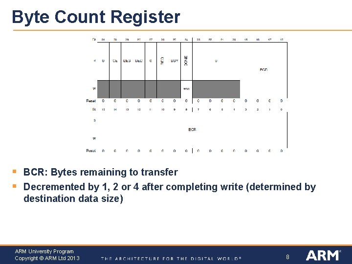
Byte Count Register § § BCR: Bytes remaining to transfer Decremented by 1, 2 or 4 after completing write (determined by destination data size) ARM University Program Copyright © ARM Ltd 2013 8
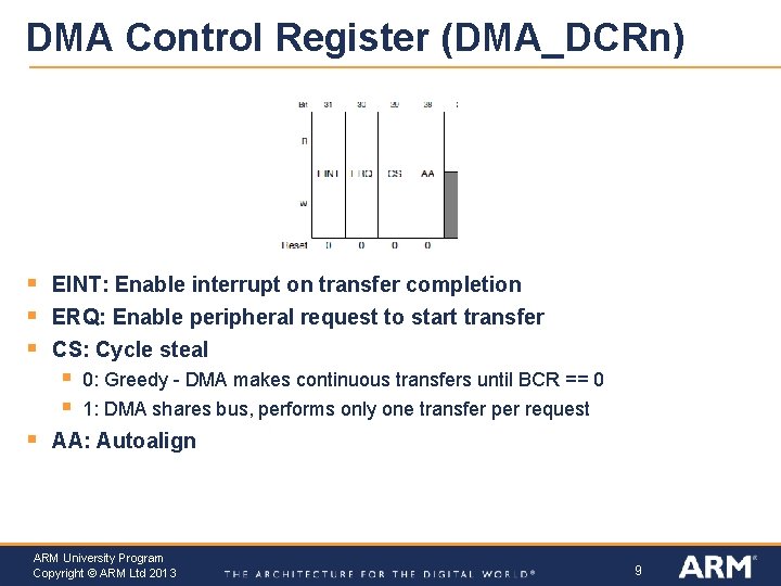
DMA Control Register (DMA_DCRn) § § § EINT: Enable interrupt on transfer completion ERQ: Enable peripheral request to start transfer CS: Cycle steal § § § 0: Greedy - DMA makes continuous transfers until BCR == 0 1: DMA shares bus, performs only one transfer per request AA: Autoalign ARM University Program Copyright © ARM Ltd 2013 9
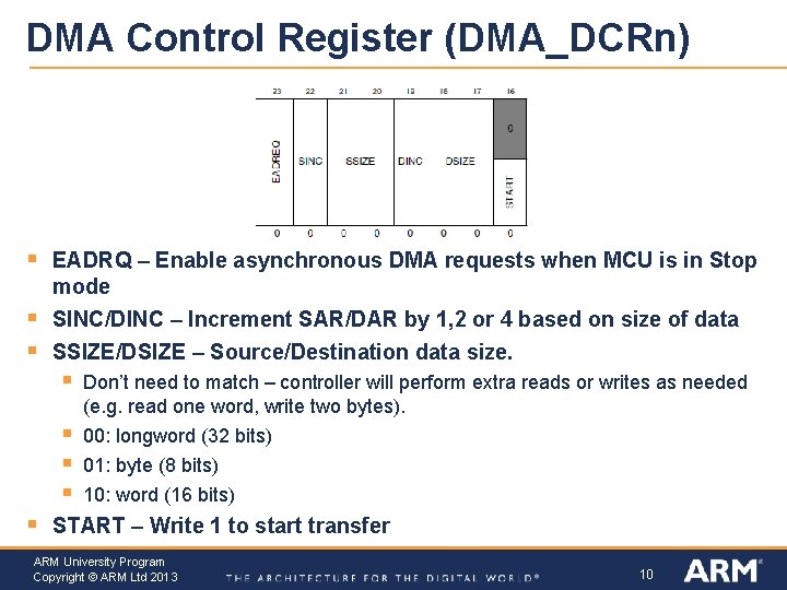
DMA Control Register (DMA_DCRn) § EADRQ – Enable asynchronous DMA requests when MCU is in Stop mode § § SINC/DINC – Increment SAR/DAR by 1, 2 or 4 based on size of data SSIZE/DSIZE – Source/Destination data size. § § § Don’t need to match – controller will perform extra reads or writes as needed (e. g. read one word, write two bytes). 00: longword (32 bits) 01: byte (8 bits) 10: word (16 bits) START – Write 1 to start transfer ARM University Program Copyright © ARM Ltd 2013 10
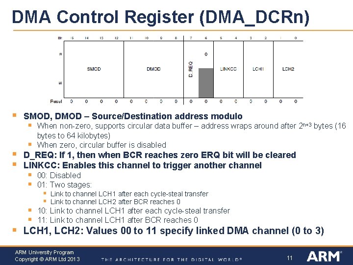
DMA Control Register (DMA_DCRn) § § SMOD, DMOD – Source/Destination address modulo § § When non-zero, supports circular data buffer – address wraps around after 2 n+3 bytes (16 bytes to 64 kilobytes) When zero, circular buffer is disabled D_REQ: If 1, then when BCR reaches zero ERQ bit will be cleared LINKCC: Enables this channel to trigger another channel § § 00: Disabled 01: Two stages: § § Link to channel LCH 1 after each cycle-steal transfer Link to channel LCH 2 after BCR reaches 0 § 10: Link to channel LCH 1 after each cycle-steal transfer § 11: Link to channel LCH 1 after BCR reaches 0 LCH 1, LCH 2: Values 00 to 11 specify linked DMA channel (0 to 3) ARM University Program Copyright © ARM Ltd 2013 11
Basic Use of DMA § § § § Enable clock to DMA module (in SIM register SCGC 7) Initialize control registers Load SARn with source address Load DARn with destination address Load BCRn with number of bytes to transfer Clear DSRn[DONE] Start transfer by setting DCRn[START] Wait for end of transfer § § Interrupt generated if DCRn[EINT] is set (DMAn_IRQHandler) Poll DSRn[DONE] ARM University Program Copyright © ARM Ltd 2013 12
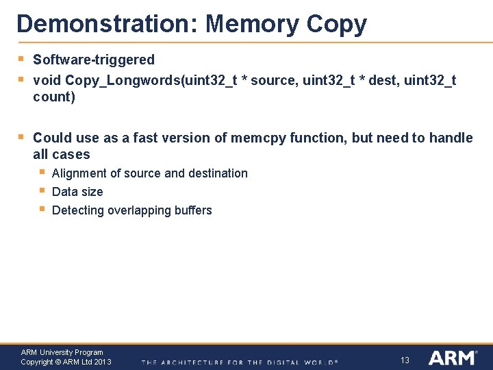
Demonstration: Memory Copy § § Software-triggered void Copy_Longwords(uint 32_t * source, uint 32_t * dest, uint 32_t count) § Could use as a fast version of memcpy function, but need to handle all cases § § § Alignment of source and destination Data size Detecting overlapping buffers ARM University Program Copyright © ARM Ltd 2013 13
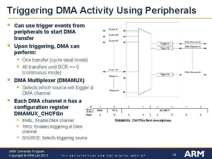
Triggering DMA Activity Using Peripherals § Can use trigger events from peripherals to start DMA transfer § Upon triggering, DMA can perform: § § § DMA Multiplexer (DMAMUX) § § One transfer (cycle steal mode) All transfers until BCR == 0 (continuous mode) Selects which source will trigger a DMA channel Each DMA channel n has a configuration register DMAMUX_CHCFGn § ENBL: Enable DMA channel § TRIG: Enables triggering of DMA § channel SOURCE: Selects triggering source ARM University Program Copyright © ARM Ltd 2013 14
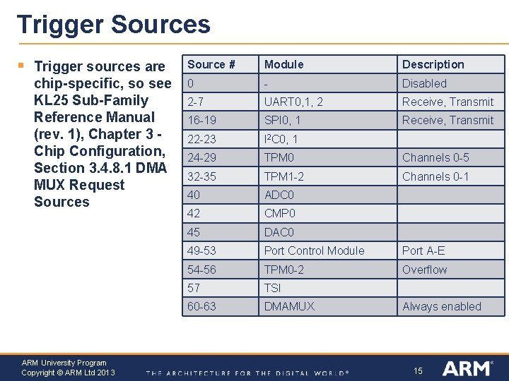
Trigger Sources § Trigger sources are chip-specific, so see KL 25 Sub-Family Reference Manual (rev. 1), Chapter 3 Chip Configuration, Section 3. 4. 8. 1 DMA MUX Request Sources ARM University Program Copyright © ARM Ltd 2013 Source # Module Description 0 - Disabled 2 -7 UART 0, 1, 2 Receive, Transmit 16 -19 SPI 0, 1 Receive, Transmit 22 -23 I 2 C 0, 1 24 -29 TPM 0 Channels 0 -5 32 -35 TPM 1 -2 Channels 0 -1 40 ADC 0 42 CMP 0 45 DAC 0 49 -53 Port Control Module Port A-E 54 -56 TPM 0 -2 Overflow 57 TSI 60 -63 DMAMUX Always enabled 15
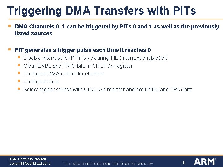
Triggering DMA Transfers with PITs § DMA Channels 0, 1 can be triggered by PITs 0 and 1 as well as the previously listed sources § PIT generates a trigger pulse each time it reaches 0 § § § Disable interrupt for PITn by clearing TIE (interrupt enable) bit. Clear ENBL and TRIG bits in CHCFGn register Configure DMA Controller channel Configure timer Select trigger source with CHCFGn register and set ENBL and TRIG bits ARM University Program Copyright © ARM Ltd 2013 16
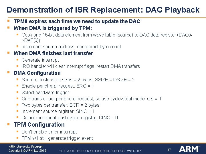
Demonstration of ISR Replacement: DAC Playback § § § TPM 0 expires each time we need to update the DAC When DMA is triggered by TPM: § § Copy one 16 -bit data element from wave table (source) to DAC data register (DAC 0>DAT[0]) Increment source address, decrement byte count When DMA finishes last transfer § § Generate interrupt IRQ handler will clear interrupt flags, restart DMA transfers DMA Configuration § Source, destination sizes = 2 bytes: SSIZE = DSIZE = 2 § Enable peripheral request: ERQ = 1 § Select hardware trigger § One transfer peripheral request, so use cycle-steal mode: CS = 1 § Two bytes per transfer: BCR = 2 bytes § Increment source register: SINC = 1 § Do not increment destination register: DINC = 0 TPM Configuration § Don’t enable timer interrupt § TPM will still generate trigger event ARM University Program Copyright © ARM Ltd 2013 17
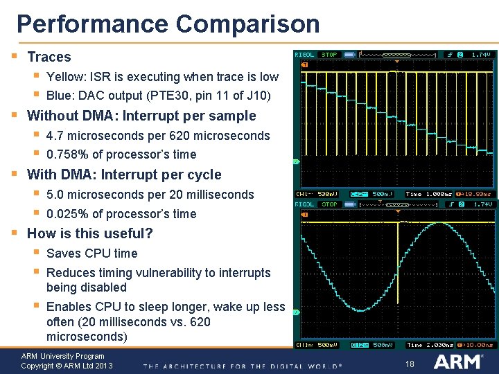
Performance Comparison § Traces § § § 4. 7 microseconds per 620 microseconds 0. 758% of processor’s time With DMA: Interrupt per cycle § § § Blue: DAC output (PTE 30, pin 11 of J 10) Without DMA: Interrupt per sample § § § Yellow: ISR is executing when trace is low 5. 0 microseconds per 20 milliseconds 0. 025% of processor’s time How is this useful? § § Saves CPU time § Enables CPU to sleep longer, wake up less often (20 milliseconds vs. 620 microseconds) Reduces timing vulnerability to interrupts being disabled ARM University Program Copyright © ARM Ltd 2013 18