Updates of clearing electrode and groove structure experiments

- Slides: 28

Updates of clearing electrode and groove structure experiments at KEKB Y. Suetsugu, KEKB Vacuum Group n n Brief review of the experiments in 2008 Clearing electrode Ver. 2 – Improvements in feed through connection n Groove structure Ver. 2 – Shallow groove – Manufacturing methods n Summaries – Future plans 2009/6/25 CESRTA 09, Cornell University 2009 1

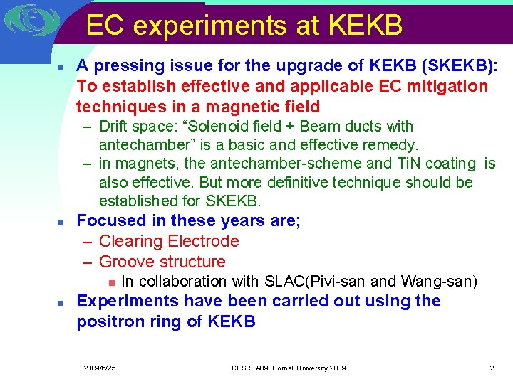
EC experiments at KEKB n A pressing issue for the upgrade of KEKB (SKEKB): To establish effective and applicable EC mitigation techniques in a magnetic field – Drift space: “Solenoid field + Beam ducts with antechamber” is a basic and effective remedy. – in magnets, the antechamber-scheme and Ti. N coating is also effective. But more definitive technique should be established for SKEKB. n Focused in these years are; – Clearing Electrode – Groove structure n n In collaboration with SLAC(Pivi-san and Wang-san) Experiments have been carried out using the positron ring of KEKB 2009/6/25 CESRTA 09, Cornell University 2009 2

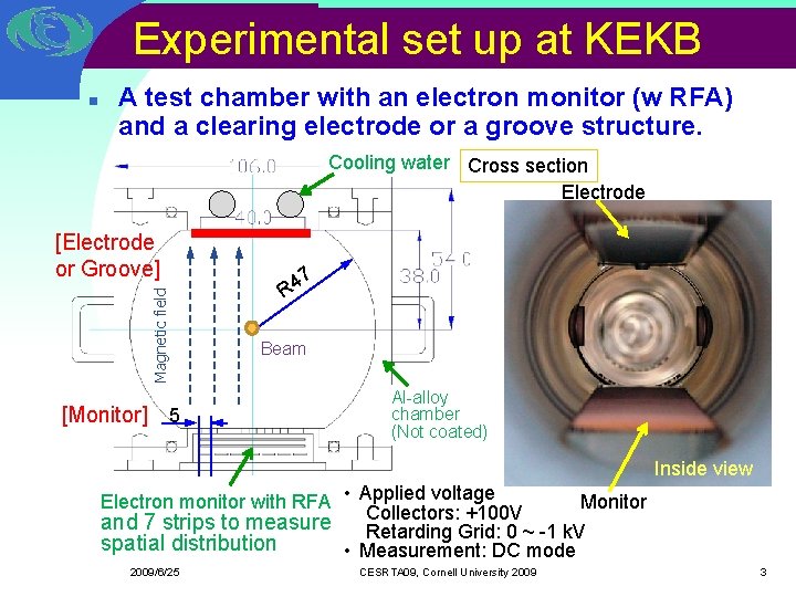
Experimental set up at KEKB n A test chamber with an electron monitor (w RFA) and a clearing electrode or a groove structure. Cooling water Cross section Electrode [Electrode or Groove] 7 Magnetic field R 4 [Monitor] Beam 5 Al-alloy chamber (Not coated) Inside view Monitor Electron monitor with RFA • Applied voltage Collectors: +100 V and 7 strips to measure Retarding Grid: 0 ~ -1 k. V spatial distribution • Measurement: DC mode 2009/6/25 CESRTA 09, Cornell University 2009 3

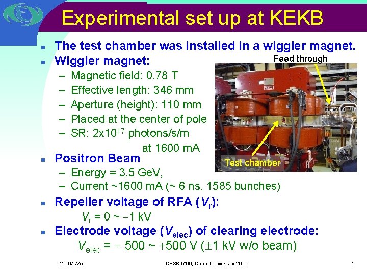
Experimental set up at KEKB n n The test chamber was installed in a wiggler magnet. Feed through Wiggler magnet: – – – n Magnetic field: 0. 78 T Effective length: 346 mm Aperture (height): 110 mm Placed at the center of pole SR: 2 x 10¹⁷ photons/s/m at 1600 m. A Positron Beam Test chamber – Energy = 3. 5 Ge. V, – Current ~1600 m. A (~ 6 ns, 1585 bunches) n Repeller voltage of RFA (Vr): Vr = 0 ~ 1 k. V n Electrode voltage (Velec) of clearing electrode: Velec = 500 ~ 500 V ( 1 k. V w/o beam) 2009/6/25 CESRTA 09, Cornell University 2009 4

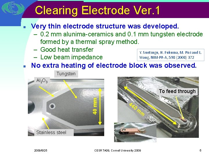
Clearing Electrode Ver. 1 n Very thin electrode structure was developed. – 0. 2 mm alunima-ceramics and 0. 1 mm tungsten electrode formed by a thermal spray method. – Good heat transfer Y. Suetsugu, H. Fukuma, M. Pivi and L. Wang, NIM-PR-A, 598 (2008) 372 – Low beam impedance No extra heating of electrode block was observed. Tungsten Al 2 O 3 To feed through 40 mm n 44 0 m m Stainless steel 2009/6/25 CESRTA 09, Cornell University 2009 5

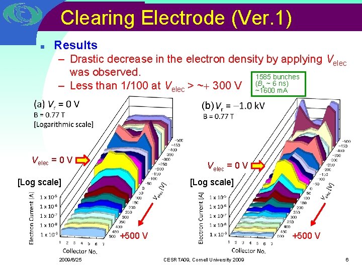
Clearing Electrode (Ver. 1) n Results – Drastic decrease in the electron density by applying Velec was observed. 1585 bunches s ~ 6 ns) – Less than 1/100 at Velec > ~ 300 V (B ~1600 m. A (b) Velec = 0 V [Log scale] +500 V 2009/6/25 +500 V CESRTA 09, Cornell University 2009 6

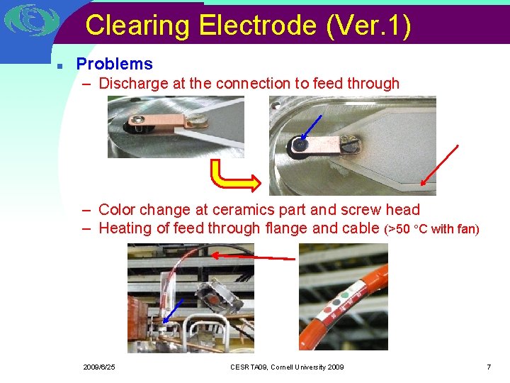
Clearing Electrode (Ver. 1) n Problems – Discharge at the connection to feed through – Color change at ceramics part and screw head – Heating of feed through flange and cable (>50 C with fan) 2009/6/25 CESRTA 09, Cornell University 2009 7

Groove structure Ver. 1 n Triangular-type groove structure, with Ti. N coating – Fabricated in SLAC n Compared with the results for a flat surface (Ti. N coated) and clearing electrode (W) Y. Suetsugu, H. Fukuma, M. Pivi and L. Wang, NIM-PR-A, 604 (2009) 449 2009/6/25 CESRTA 09, Cornell University 2009 8

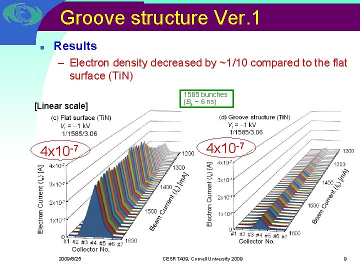
Groove structure Ver. 1 n Results – Electron density decreased by ~1/10 compared to the flat surface (Ti. N) [Linear scale] 4 x 10 -7 2009/6/25 1585 bunches (Bs ~ 6 ns) 4 x 10 -7 CESRTA 09, Cornell University 2009 9

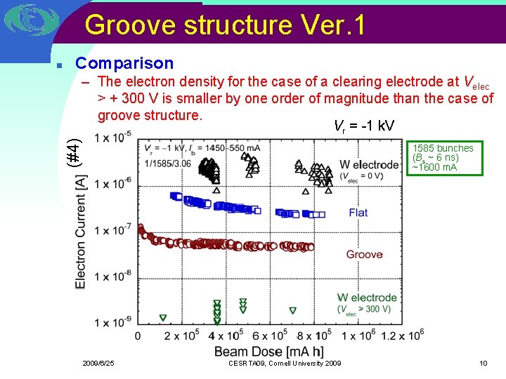
Groove structure Ver. 1 Comparison – The electron density for the case of a clearing electrode at Velec > + 300 V is smaller by one order of magnitude than the case of groove structure. Vr = -1 k. V (#4) n 1585 bunches (Bs ~ 6 ns) ~1600 m. A 2009/6/25 CESRTA 09, Cornell University 2009 10

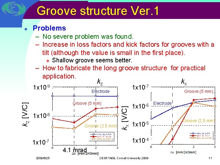
Groove structure Ver. 1 n Problems – No severe problem was found. – Increase in loss factors and kick factors for grooves with a tilt (although the value is small in the first place). n Shallow groove seems better. – How to fabricate the long groove structure for practical application. kz Electrode Groove (5 mm) 1 x 10 -8 Groove (2. 5 mm) kx 1 x 10 -7 kx [V/C] kz [V/C] 1 x 10 -9 1 x 10 -6 1 x 10 -5 Groove (5 mm) Electrode Groove (2. 5 mm) 1 x 10 -4 1 x 10 -7 4. 1 mrad 2009/6/25 CESRTA 09, Cornell University 2009 11

Experiments in 2009 n n Improved versions of the clearing electrode and the groove structure were tested in the spring run. Clearing electrode Ver. 2 – Improvements in feed through connection n Groove structure Ver. 2 – Shallow groove – R&D on the manufacturing methods 2009/6/25 CESRTA 09, Cornell University 2009 12

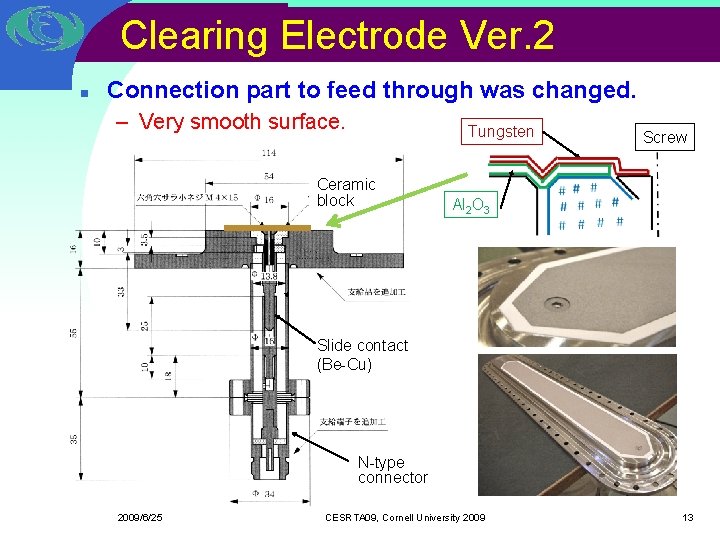
Clearing Electrode Ver. 2 n Connection part to feed through was changed. – Very smooth surface. Tungsten Ceramic block Screw Al 2 O 3 Slide contact (Be-Cu) N-type connector 2009/6/25 CESRTA 09, Cornell University 2009 13

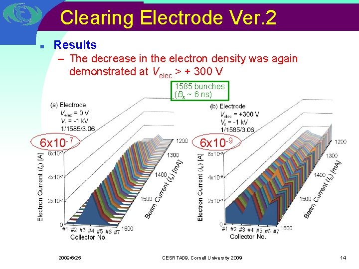
Clearing Electrode Ver. 2 n Results – The decrease in the electron density was again demonstrated at Velec > + 300 V 1585 bunches (Bs ~ 6 ns) 6 x 10 -7 2009/6/25 6 x 10 -9 CESRTA 09, Cornell University 2009 14

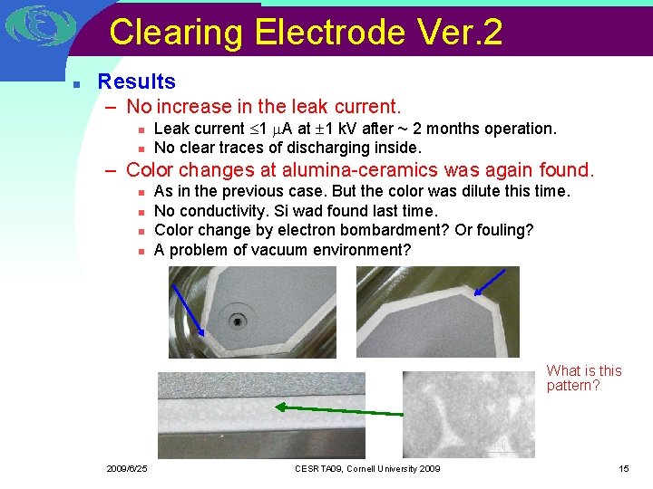
Clearing Electrode Ver. 2 n Results – No increase in the leak current. n n Leak current 1 m. A at 1 k. V after ~ 2 months operation. No clear traces of discharging inside. – Color changes at alumina-ceramics was again found. n n As in the previous case. But the color was dilute this time. No conductivity. Si wad found last time. Color change by electron bombardment? Or fouling? A problem of vacuum environment? What is this pattern? 2009/6/25 CESRTA 09, Cornell University 2009 15

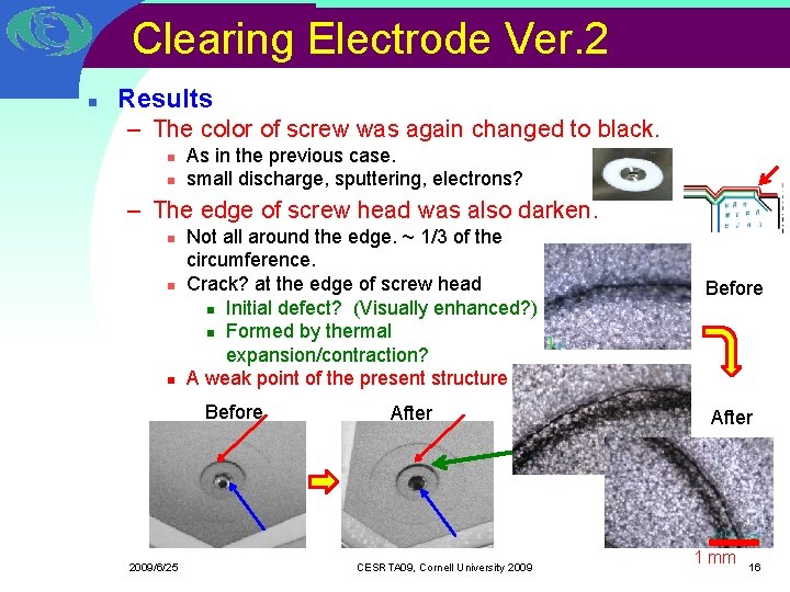
Clearing Electrode Ver. 2 n Results – The color of screw was again changed to black. n n As in the previous case. small discharge, sputtering, electrons? – The edge of screw head was also darken. n n n Not all around the edge. ~ 1/3 of the circumference. Crack? at the edge of screw head n Initial defect? (Visually enhanced? ) n Formed by thermal expansion/contraction? A weak point of the present structure Before 2009/6/25 After CESRTA 09, Cornell University 2009 Before After 1 mm 16

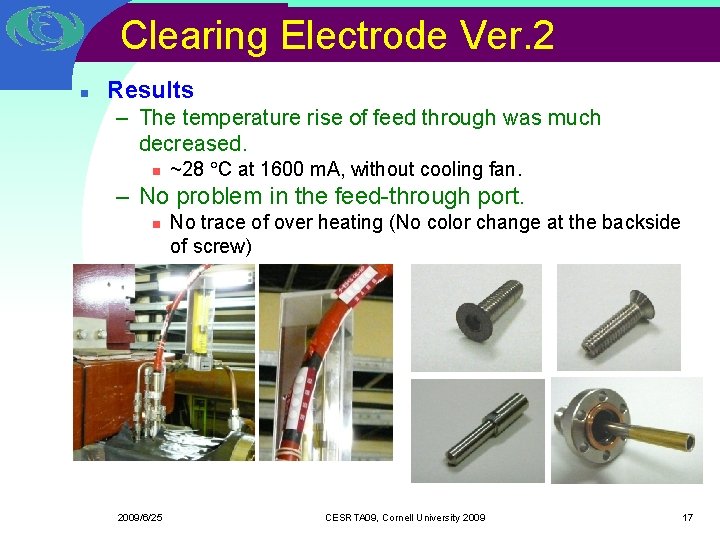
Clearing Electrode Ver. 2 n Results – The temperature rise of feed through was much decreased. n ~28 C at 1600 m. A, without cooling fan. – No problem in the feed-through port. n 2009/6/25 No trace of over heating (No color change at the backside of screw) CESRTA 09, Cornell University 2009 17

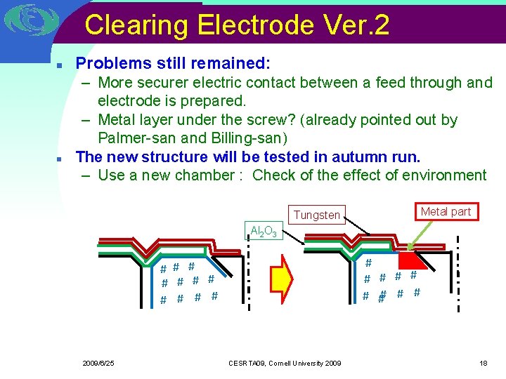
Clearing Electrode Ver. 2 n n Problems still remained: – More securer electric contact between a feed through and electrode is prepared. – Metal layer under the screw? (already pointed out by Palmer-san and Billing-san) The new structure will be tested in autumn run. – Use a new chamber : Check of the effect of environment Metal part Tungsten Al 2 O 3 # # # ## # # # 2009/6/25 CESRTA 09, Cornell University 2009 18

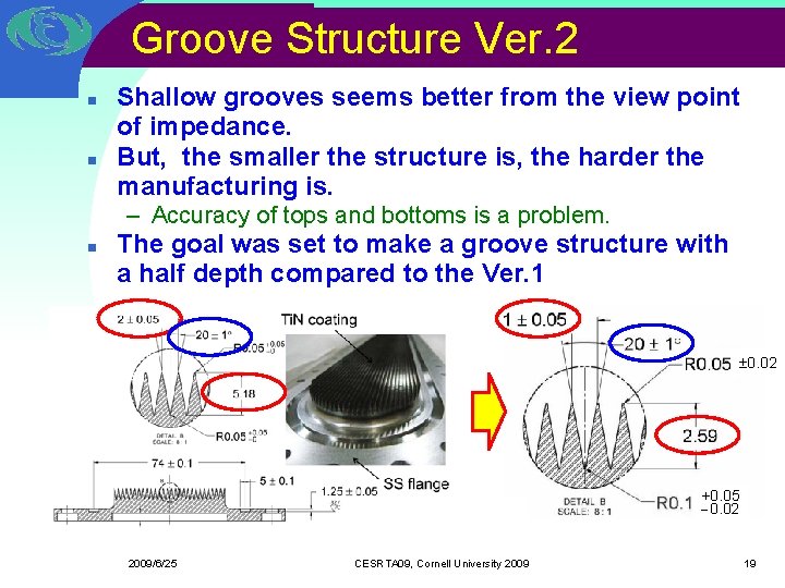
Groove Structure Ver. 2 n n Shallow grooves seems better from the view point of impedance. But, the smaller the structure is, the harder the manufacturing is. – Accuracy of tops and bottoms is a problem. n The goal was set to make a groove structure with a half depth compared to the Ver. 1 0. 02 +0. 05 0. 02 2009/6/25 CESRTA 09, Cornell University 2009 19

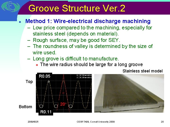
Groove Structure Ver. 2 n Method 1: Wire-electrical discharge machining – Low price compared to the machining, especially for stainless steel (depends on material). – Rough surface, may be good for SEY. – The roundness of valley is determined by the size of wire used. – Long grove is difficult to manufacture. n The wire radius should be large for a long groove Stainless steel model R 0. 05 Top 20 Bottom R 0. 11 2009/6/25 CESRTA 09, Cornell University 2009 20

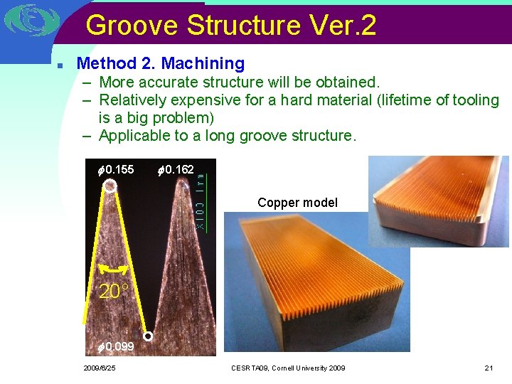
Groove Structure Ver. 2 n Method 2. Machining – More accurate structure will be obtained. – Relatively expensive for a hard material (lifetime of tooling is a big problem) – Applicable to a long groove structure. f 0. 155 f 0. 162 Copper model 20° f 0. 099 2009/6/25 CESRTA 09, Cornell University 2009 21

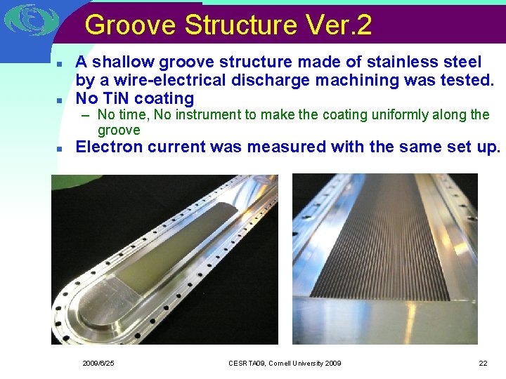
Groove Structure Ver. 2 n n A shallow groove structure made of stainless steel by a wire-electrical discharge machining was tested. No Ti. N coating – No time, No instrument to make the coating uniformly along the groove n Electron current was measured with the same set up. 2009/6/25 CESRTA 09, Cornell University 2009 22

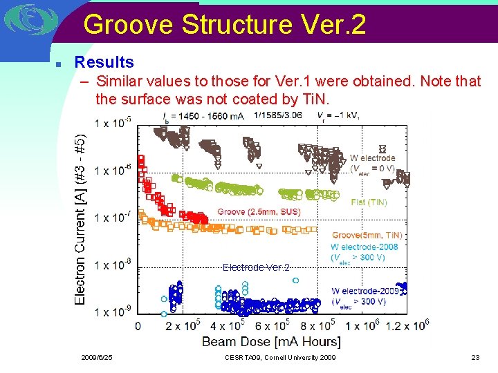
Groove Structure Ver. 2 n Results – Similar values to those for Ver. 1 were obtained. Note that the surface was not coated by Ti. N. Electrode Ver. 2 2009/6/25 CESRTA 09, Cornell University 2009 23

Summaries n n Based on the experiments last year, the improved clearing electrode and the shallow groove structure were tested. Clearing electrode Ver. 2: – The problems found before was much improved. – Still remained are the more reliability of connection part and the understanding of color change. n Groove structure Ver. 2: – A groove with a depth of ~2. 5 mm seems promising. – The similar effect to the 5 mm depth was found. – Manufacturing by wire-electrical discharge machining or machining is both available. – If material is aluminum alloy, the machining seems better. n The experiment will be carried again in the autumn run, which will be the final one for the KEKB. 2009/6/25 CESRTA 09, Cornell University 2009 24

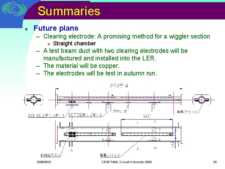
Summaries n Future plans – Clearing electrode: A promising method for a wiggler section n Straight chamber – A test beam duct with two clearing electrodes will be manufactured and installed into the LER. – The material will be copper. – The electrodes will be test in autumn run. 2009/6/25 CESRTA 09, Cornell University 2009 25

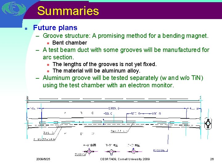
Summaries n Future plans – Groove structure: A promising method for a bending magnet. n Bent chamber – A test beam duct with some grooves will be manufactured for arc section. n n The lengths of the grooves is not yet fixed. The material will be aluminum alloy. – Aluminum groove will be tested separately (w and w/o Ti. N) using the test chamber with an electron monitor. 2009/6/25 CESRTA 09, Cornell University 2009 26

END 2009/6/25 CESRTA 09, Cornell University 2009 27

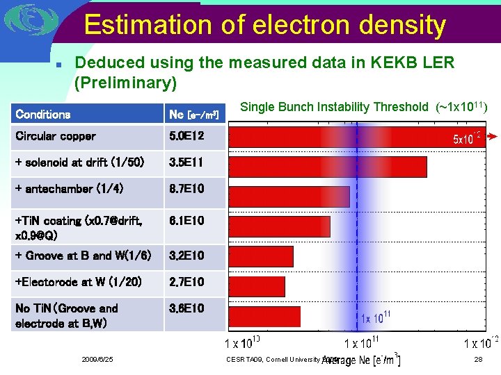
Estimation of electron density n Deduced using the measured data in KEKB LER (Preliminary) Conditions Ne Circular copper 5. 0 E 12 + solenoid at drift (1/50) 3. 5 E 11 + antechamber (1/4) 8. 7 E 10 +Ti. N coating (x 0. 7@drift, x 0. 9@Q) 6. 1 E 10 + Groove at B and W(1/6) 3. 2 E 10 +Electorode at W (1/20) 2. 7 E 10 No Ti. N(Groove and electrode at B, W) 3. 6 E 10 2009/6/25 [e-/m 3] Single Bunch Instability Threshold (~1 x 10¹¹) CESRTA 09, Cornell University 2009 28