University Workshop Introduction to Internal External FPGA Memory




- Slides: 34

University Workshop: Introduction to Internal & External FPGA Memory January 2019

Objectives Understand basics of RAM memory § SRAM vs. DRAM vs. SDRAM § SDRAM evolution Understand basics of FPGA on-chip RAM memory § MLAB, M 9 K, M 20 K, and e. SRAM Understand basics of SDRAM memory § How is the memory organized, how does it operate? Programmable Solutions Group Intel Confidential 2

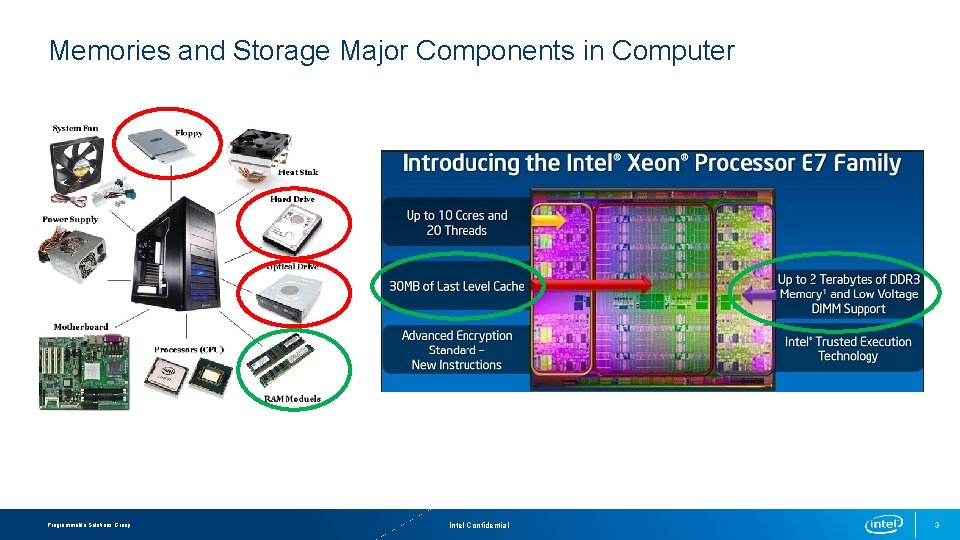
Memories and Storage Major Components in Computer Programmable Solutions Group Intel Confidential 3

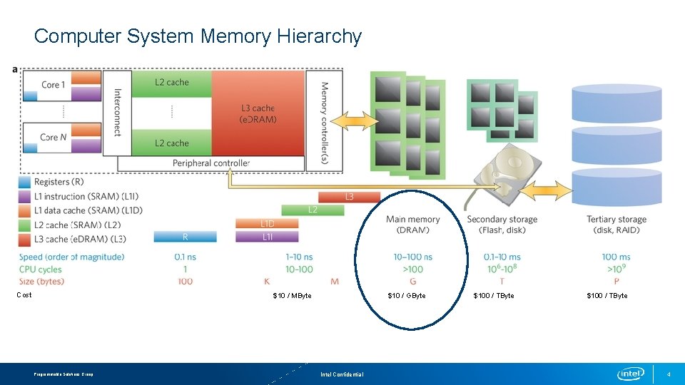
Computer System Memory Hierarchy Cost $10 / GByte $10 / MByte Programmable Solutions Group Intel Confidential $100 / TByte 4

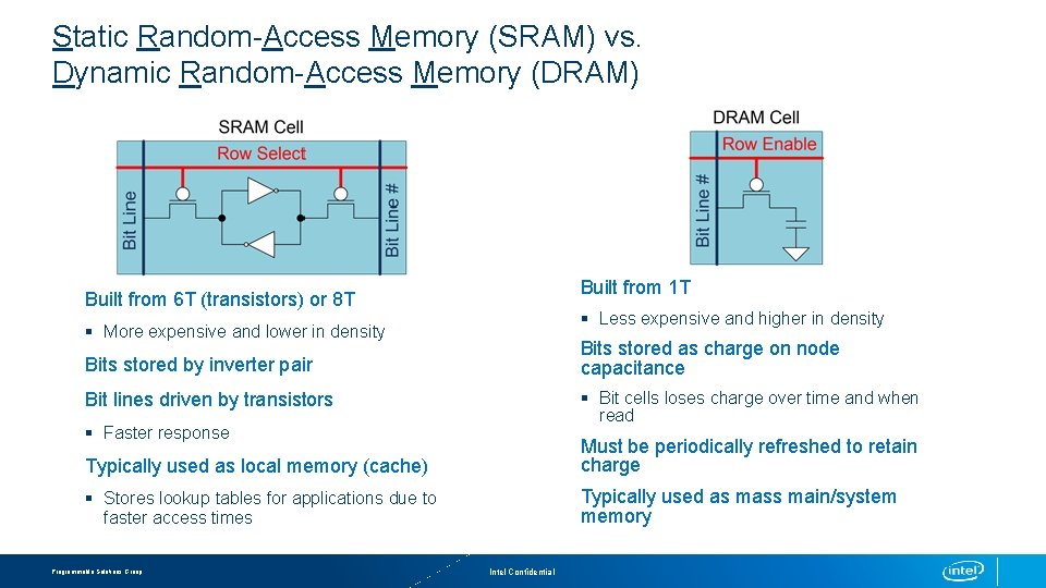
Static Random-Access Memory (SRAM) vs. Dynamic Random-Access Memory (DRAM) Built from 1 T Built from 6 T (transistors) or 8 T § Less expensive and higher in density § More expensive and lower in density Bits stored by inverter pair Bits stored as charge on node capacitance Bit lines driven by transistors § Bit cells loses charge over time and when read § Faster response Typically used as local memory (cache) Must be periodically refreshed to retain charge § Stores lookup tables for applications due to faster access times Typically used as mass main/system memory Programmable Solutions Group Intel Confidential

FPGA On-Chip Memory Basics

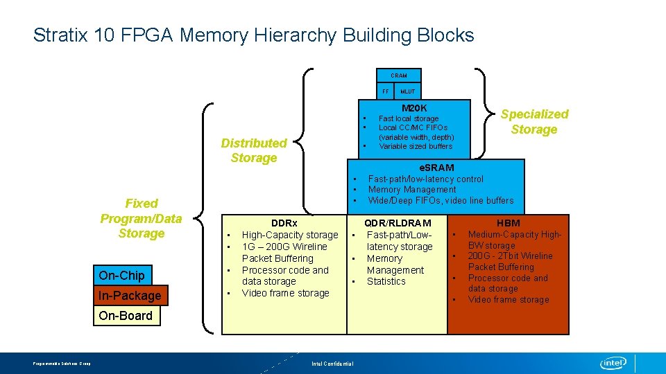
Stratix 10 FPGA Memory Hierarchy Building Blocks CRAM FF MLUT M 20 K • • Distributed Storage Fixed Program/Data Storage • On-Chip • In-Package • DDRx High-Capacity storage 1 G – 200 G Wireline Packet Buffering Processor code and data storage Video frame storage Fast-path/low-latency control Memory Management Wide/Deep FIFOs, video line buffers QDR/RLDRAM • Fast-path/Lowlatency storage • Memory Management • Statistics On-Board Programmable Solutions Group Specialized Storage e. SRAM • • • Fast local storage Local CC/MC FIFOs (variable width, depth) Variable sized buffers Intel Confidential HBM • • Medium-Capacity High. BW storage 200 G - 2 Tbit Wireline Packet Buffering Processor code and data storage Video frame storage

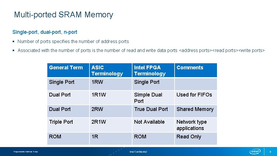
Multi-ported SRAM Memory Single-port, dual-port, n-port § Number of ports specifies the number of address ports § Associated with the number of ports is the number of read and write data ports <address ports><read ports><write ports> Programmable Solutions Group General Term ASIC Terminology Intel FPGA Terminology Single Port 1 RW Single Port Dual Port 1 R 1 W Simple Dual Port Used for FIFOs Dual Port 2 RW True Dual Port Shared Memory Triple Port 2 R 1 W Not Available Network type applications ROM 1 R ROM Read Only Intel Confidential Comments 8

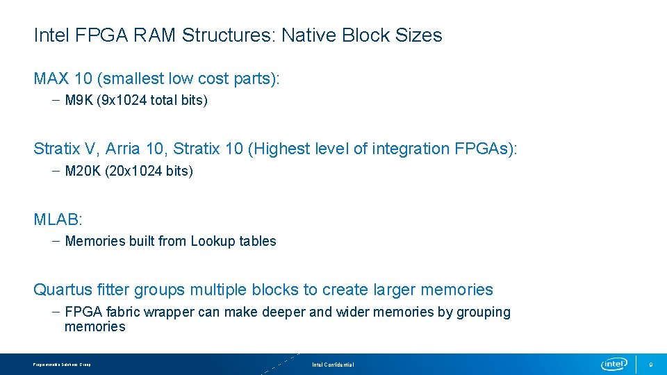
Intel FPGA RAM Structures: Native Block Sizes MAX 10 (smallest low cost parts): – M 9 K (9 x 1024 total bits) Stratix V, Arria 10, Stratix 10 (Highest level of integration FPGAs): – M 20 K (20 x 1024 bits) MLAB: – Memories built from Lookup tables Quartus fitter groups multiple blocks to create larger memories – FPGA fabric wrapper can make deeper and wider memories by grouping memories Programmable Solutions Group Intel Confidential 9

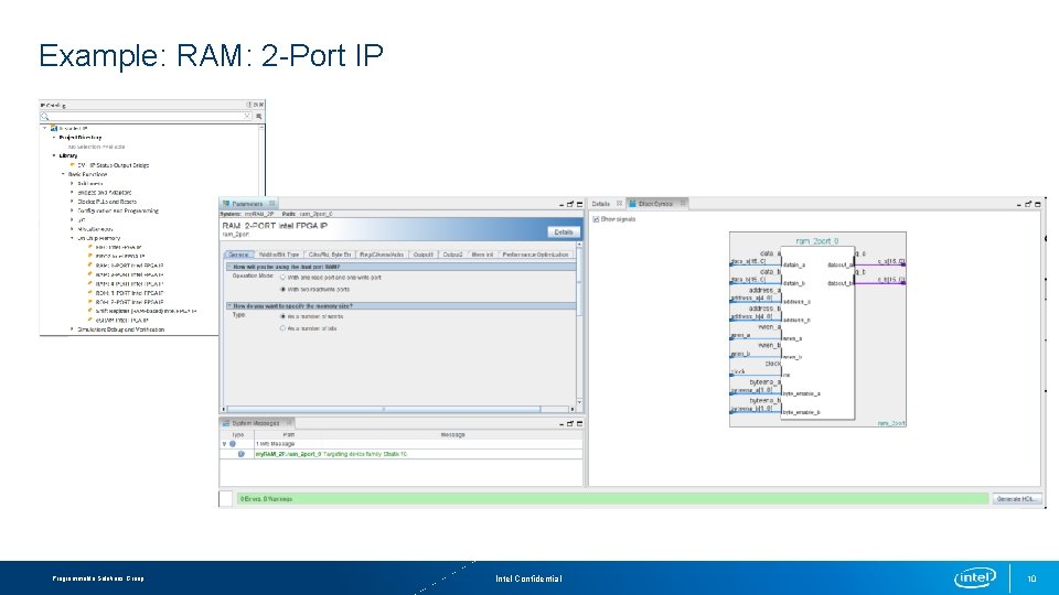
Example: RAM: 2 -Port IP Programmable Solutions Group Intel Confidential 10

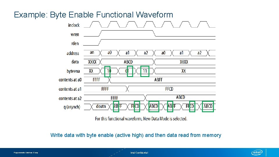
Example: Byte Enable Functional Waveform Write data with byte enable (active high) and then data read from memory Programmable Solutions Group Intel Confidential

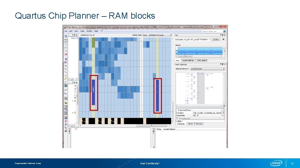
Quartus Chip Planner – RAM blocks Programmable Solutions Group Intel Confidential 12

SDRAM Memory Basics (DDR 3 as an example)

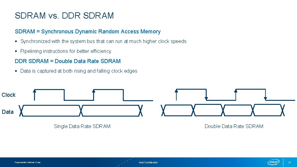
SDRAM vs. DDR SDRAM = Synchronous Dynamic Random Access Memory § Synchronized with the system bus that can run at much higher clock speeds § Pipelining instructions for better efficiency DDR SDRAM = Double Data Rate SDRAM § Data is captured at both rising and falling clock edges Clock Data Single Data Rate SDRAM Programmable Solutions Group Double Data Rate SDRAM Intel Confidential 14

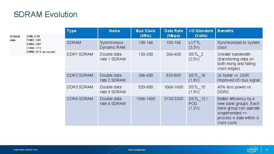
SDRAM Evolution Type Programmable Solutions Group Name Bus Clock (MHz) Data Rate (Mbps) I/O Standard (Volts) Benefits SDRAM Synchronous Dynamic RAM 100 -166 LVTTL (3. 3 V) Synchronized to system clock DDR 1 SDRAM Double data rate 1 SDRAM 133 -200 266 -400 SSTL_2 (2. 5 V) Greater bandwidth (transferring data on both rising and falling clock edges) DDR 2 SDRAM Double data rate 2 SDRAM 266 -400 533 -800 SSTL_18 (1. 8 V) 2 x faster vs. DDR. Improved I/O bus signal. DDR 3 SDRAM Double data rate 3 SDRAM 533 -800 1066 -1600 SSTL_15 (1. 5 V) 40% less power vs. DDR 2. DDR 4 SDRAM Double data rate 4 SDRAM 1066 -1600 2133 -3200 SSTL_12 / POD (1. 2 V) Better efficiency by 4 new bank groups. Each bank group can operate singlehanded => process 4 data within a clock cycle. Intel Confidential 15

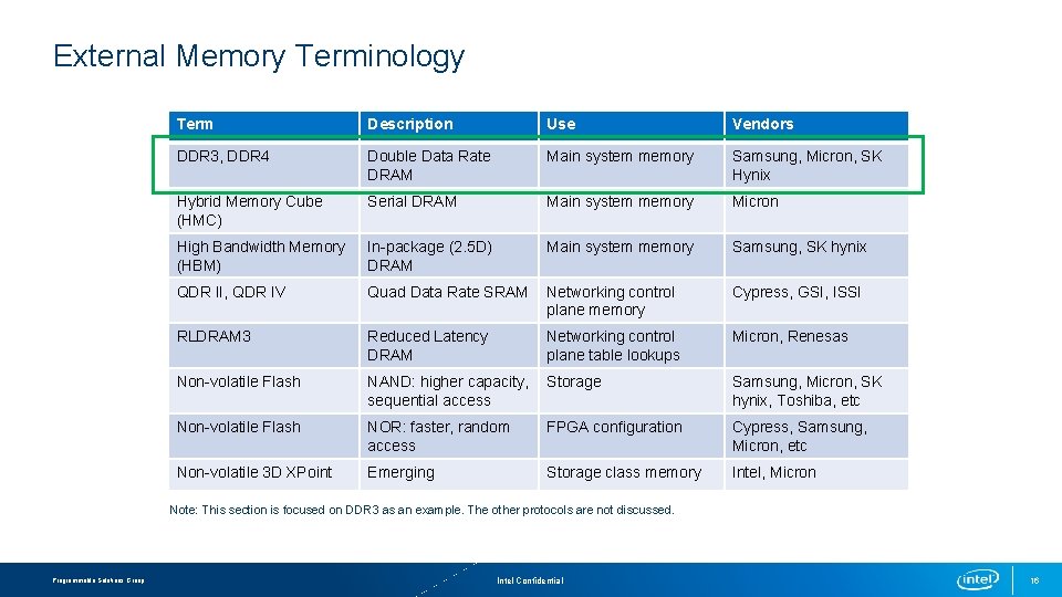
External Memory Terminology Term Description Use Vendors DDR 3, DDR 4 Double Data Rate DRAM Main system memory Samsung, Micron, SK Hynix Hybrid Memory Cube (HMC) Serial DRAM Main system memory Micron High Bandwidth Memory (HBM) In-package (2. 5 D) DRAM Main system memory Samsung, SK hynix QDR II, QDR IV Quad Data Rate SRAM Networking control plane memory Cypress, GSI, ISSI RLDRAM 3 Reduced Latency DRAM Networking control plane table lookups Micron, Renesas Non-volatile Flash NAND: higher capacity, sequential access Storage Samsung, Micron, SK hynix, Toshiba, etc Non-volatile Flash NOR: faster, random access FPGA configuration Cypress, Samsung, Micron, etc Non-volatile 3 D XPoint Emerging Storage class memory Intel, Micron Note: This section is focused on DDR 3 as an example. The other protocols are not discussed. Programmable Solutions Group Intel Confidential 16

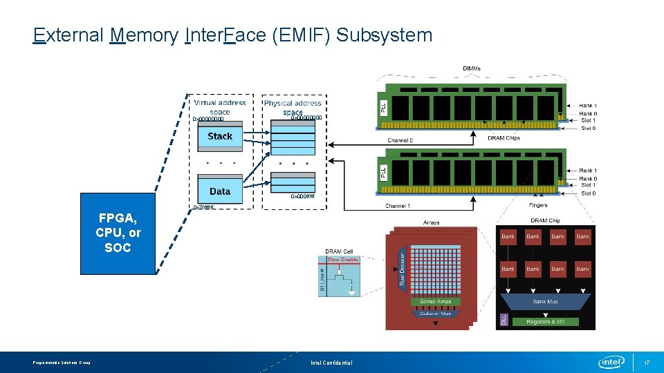
External Memory Inter. Face (EMIF) Subsystem 0 x 00000000 0 x 000 fffff 0 x 7 fffffff FPGA, CPU, or SOC Programmable Solutions Group Intel Confidential 17

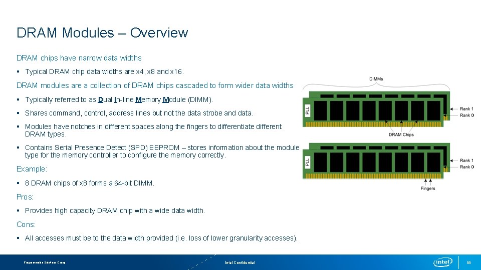
DRAM Modules – Overview DRAM chips have narrow data widths § Typical DRAM chip data widths are x 4, x 8 and x 16. DRAM modules are a collection of DRAM chips cascaded to form wider data widths § Typically referred to as Dual In-line Memory Module (DIMM). § Shares command, control, address lines but not the data strobe and data. § Modules have notches in different spaces along the fingers to differentiate different DRAM types. § Contains Serial Presence Detect (SPD) EEPROM – stores information about the module type for the memory controller to configure the memory correctly. Example: § 8 DRAM chips of x 8 forms a 64 -bit DIMM. Pros: § Provides high capacity DRAM chip with a wide data width. Cons: § All accesses must be to the data width provided (i. e. loss of lower granularity accesses). Programmable Solutions Group Intel Confidential 18

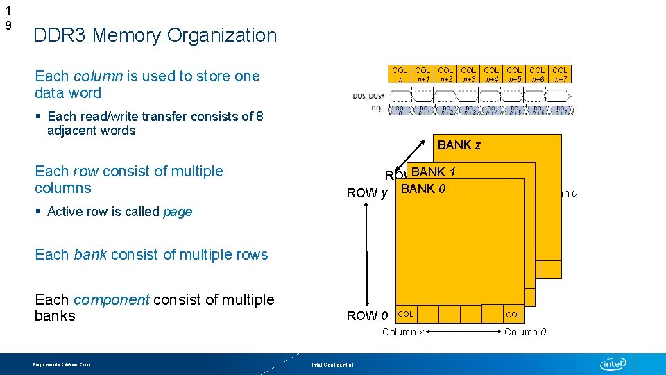
1 9 DDR 3 Memory Organization COL COL n n+1 n+2 n+3 n+4 n+5 n+6 n+7 Each column is used to store one data word § Each read/write transfer consists of 8 adjacent words Each row consist of multiple columns BANK z COL 1 ROWBANK 0 x Column ROW y BANK COL Column 0 § Active row is called page Each bank consist of multiple rows COL Each component consist of multiple banks COL ROW 0 COL Column x Programmable Solutions Group Intel Confidential COL Column 0

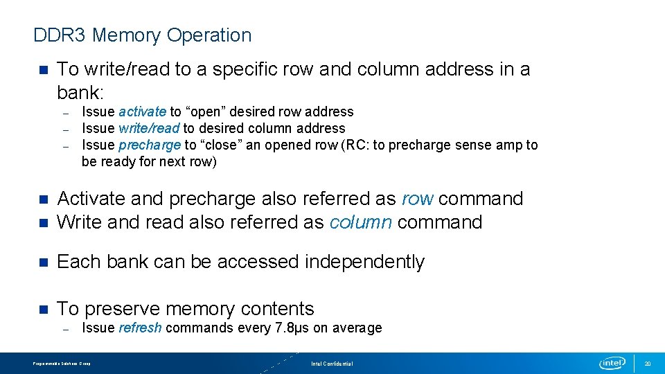
DDR 3 Memory Operation n To write/read to a specific row and column address in a bank: – – – Issue activate to “open” desired row address Issue write/read to desired column address Issue precharge to “close” an opened row (RC: to precharge sense amp to be ready for next row) n Activate and precharge also referred as row command Write and read also referred as column command n Each bank can be accessed independently n To preserve memory contents n – Issue refresh commands every 7. 8µs on average Programmable Solutions Group Intel Confidential 20

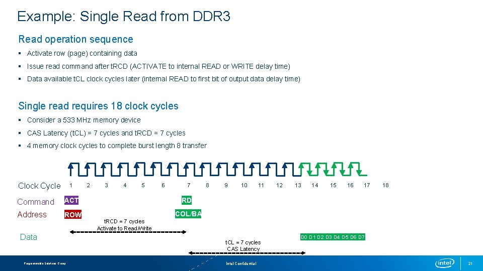
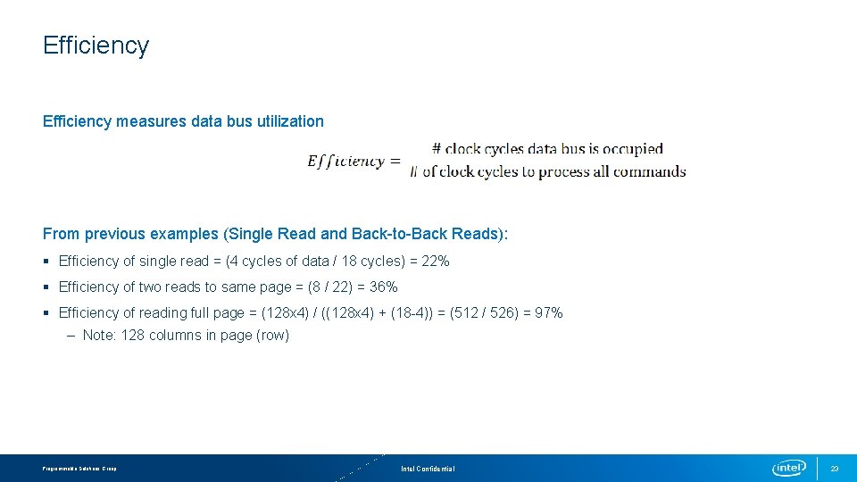
Example: Single Read from DDR 3 Read operation sequence § Activate row (page) containing data § Issue read command after t. RCD (ACTIVATE to internal READ or WRITE delay time) § Data available t. CL clock cycles later (internal READ to first bit of output data delay time) Single read requires 18 clock cycles § Consider a 533 MHz memory device § CAS Latency (t. CL) = 7 cycles and t. RCD = 7 cycles § 4 memory clock cycles to complete burst length 8 transfer Clock Cycle 1 2 3 4 5 6 7 Command ACT RD Address ROW COL/BA Data Programmable Solutions Group 8 9 10 11 12 13 14 15 16 17 18 t. RCD = 7 cycles Activate to Read/Write t. CL = 7 cycles CAS Latency Intel Confidential D 0 D 1 D 2 D 3 D 4 D 5 D 6 D 7 21

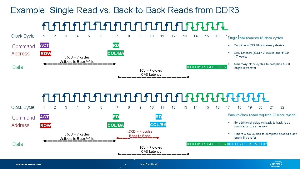
Example: Single Read vs. Back-to-Back Reads from DDR 3 Clock Cycle 1 Command Address ACT 2 ROW 3 4 5 6 t. RCD = 7 cycles Activate to Read/Write 7 8 9 10 11 12 § CAS Latency (t. CL) = 7 cycles and t. RCD = 7 cycles § 4 memory clock cycles to complete burst length 8 transfer Command ACT RD RD Address ROW COL/BA t. RCD = 7 cycles Activate to Read/Write Data Programmable Solutions Group 6 17 18 Single read requires 18 clock cycles COL/BA 1 5 16 Consider a 533 MHz memory device Clock Cycle 4 15 § D 0 D 1 D 2 D 3 D 4 D 5 D 6 D 7 t. CL = 7 cycles CAS Latency 3 14 RD Data 2 13 7 8 9 10 11 t. CCD = 4 cycles Read to Read t. CL = 7 cycles CAS Latency Intel Confidential 12 13 14 15 16 17 18 19 20 21 22 Back-to-Back reads requires 22 clock cycles § No additional delay on back to back read commands to same row § 4 more clock cycles to complete second burst length 8 transfer D 0 D 1 D 2 D 3 D 4 D 5 D 6 D 7

Efficiency measures data bus utilization From previous examples (Single Read and Back-to-Back Reads): § Efficiency of single read = (4 cycles of data / 18 cycles) = 22% § Efficiency of two reads to same page = (8 / 22) = 36% § Efficiency of reading full page = (128 x 4) / ((128 x 4) + (18 -4)) = (512 / 526) = 97% – Note: 128 columns in page (row) Programmable Solutions Group Intel Confidential 23

External Memory Interface IP Solution 24

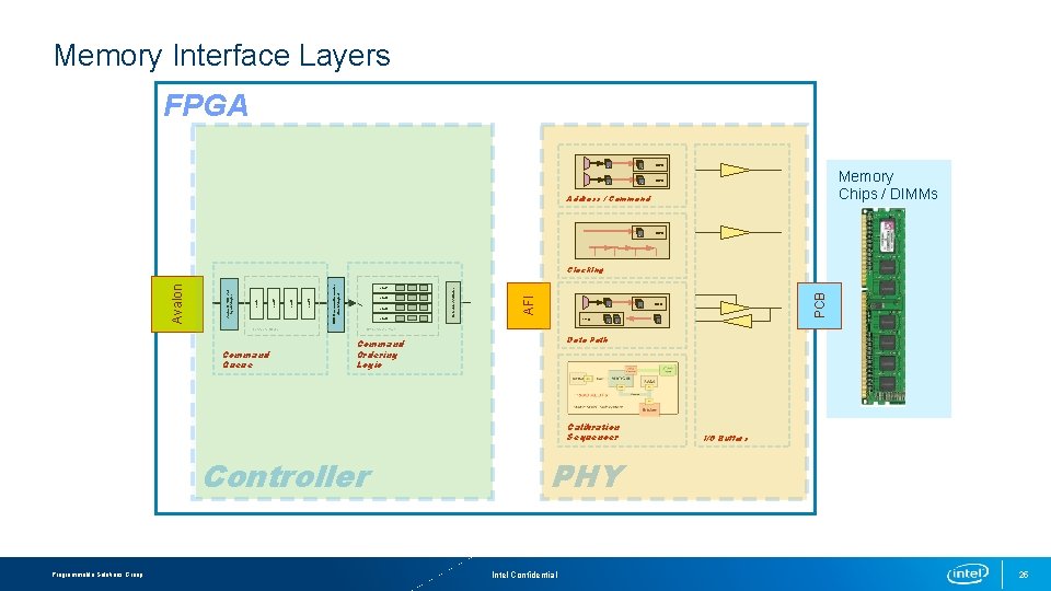
Memory Interface Layers FPGA DDIO Memory Chips / DIMMs DDIO Address / Command DDIO Command Queue cmd 2 cmd 0 DDIO FIFO TBP Command Pool Data Path Command Ordering Logic Calibration Sequencer Controller Programmable Solutions Group PCB cmd 3 AFI cmd 1 Scheduler/Arbitrator DDR Command Generator (Burst Adaptor) cmd 4 cmd 5 cmd 6 cmd 7 Avalon-ST/MM AXI Input Adaptor Avalon Clocking I/O Buffers PHY Intel Confidential 25

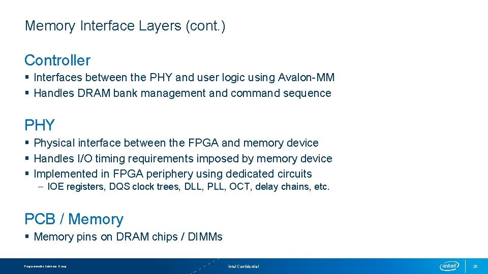
Memory Interface Layers (cont. ) Controller § Interfaces between the PHY and user logic using Avalon-MM § Handles DRAM bank management and command sequence PHY § Physical interface between the FPGA and memory device § Handles I/O timing requirements imposed by memory device § Implemented in FPGA periphery using dedicated circuits – IOE registers, DQS clock trees, DLL, PLL, OCT, delay chains, etc. PCB / Memory § Memory pins on DRAM chips / DIMMs Programmable Solutions Group Intel Confidential 26

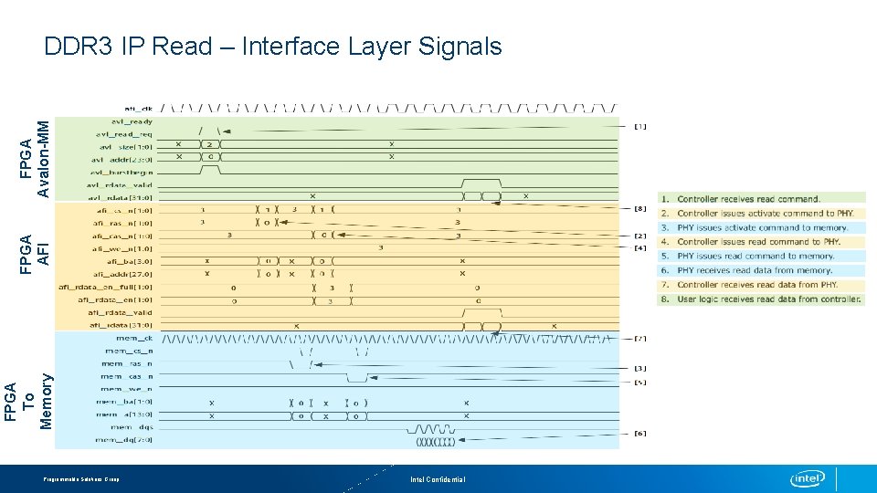
FPGA To Memory FPGA AFI FPGA Avalon-MM DDR 3 IP Read – Interface Layer Signals Programmable Solutions Group Intel Confidential

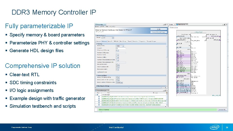
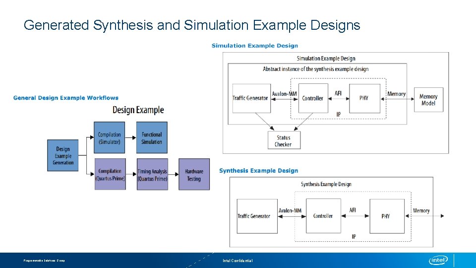
DDR 3 Memory Controller IP Fully parameterizable IP § Specify memory & board parameters § Parameterize PHY & controller settings § Generate HDL design files Comprehensive IP solution § Clear-text RTL § SDC timing constraints § I/O logic assignments § Example design with traffic generator § Simulation testbench and scripts Programmable Solutions Group Intel Confidential 28

Generated Synthesis and Simulation Example Designs Programmable Solutions Group Intel Confidential

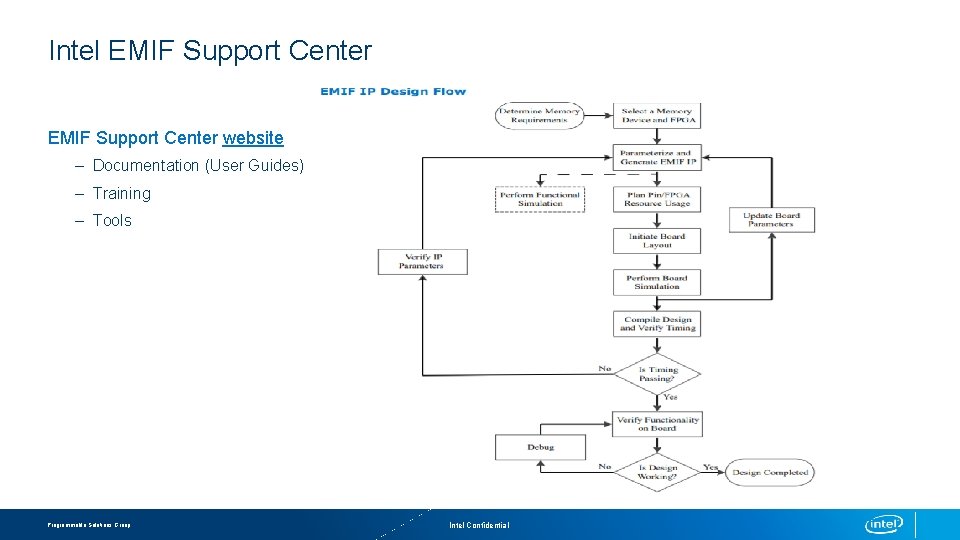
Intel EMIF Support Center website – Documentation (User Guides) – Training – Tools Programmable Solutions Group Intel Confidential

Lab Preview

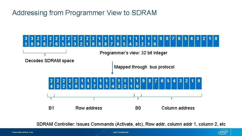
Addressing from Programmer View to SDRAM 3 3 2 2 2 2 2 1 1 1 1 1 9 8 7 6 5 4 3 2 1 0 Programmer’s view: 32 bit integer Decodes SDRAM space Mapped through bus protocol 2 2 2 1 1 1 1 1 9 8 7 6 5 4 3 2 1 0 B 1 Row address B 0 Column address SDRAM Controller: Issues Commands (Activate, etc), Row addr, column addr 1, column 2, etc Programmable Solutions Group Intel Confidential

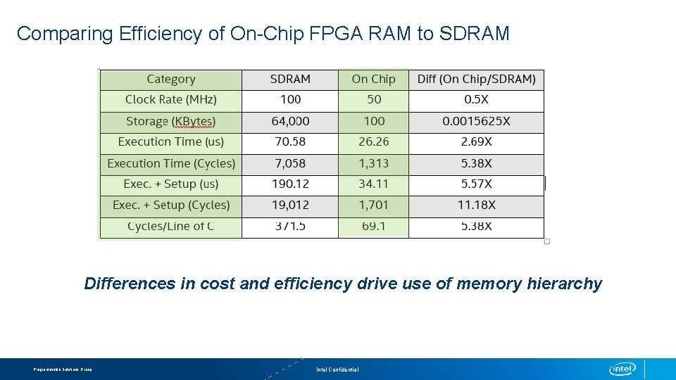
Comparing Efficiency of On-Chip FPGA RAM to SDRAM Differences in cost and efficiency drive use of memory hierarchy Programmable Solutions Group Intel Confidential

Thank you