University Womens Polytechnic AMU Aligarh ELECTRONIC DEVICES CIRCUITSII

- Slides: 48

University Women’s Polytechnic AMU Aligarh ELECTRONIC DEVICES & CIRCUITS-II (WLE-201) Unit-III: TRANSISTOR BIASING Presented By: Shahnawaz Uddin

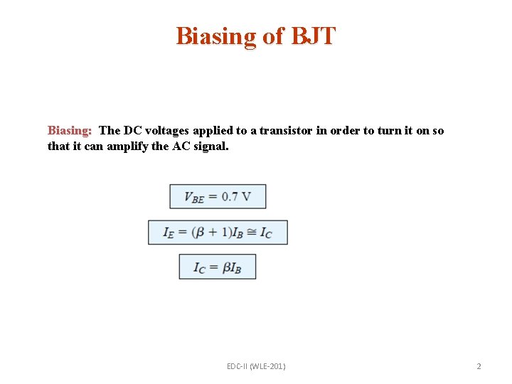
Biasing of BJT Biasing: The T DC voltages applied to a transistor in order to turn it on so that it can amplify the AC signal. EDC-II (WLE-201) 2

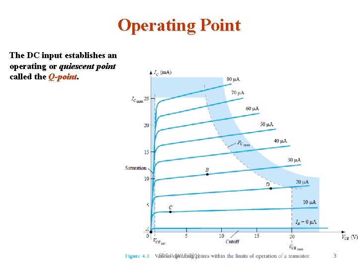
Operating Point The DC input establishes an operating or quiescent point called the Q-point EDC-II (WLE-201) 3

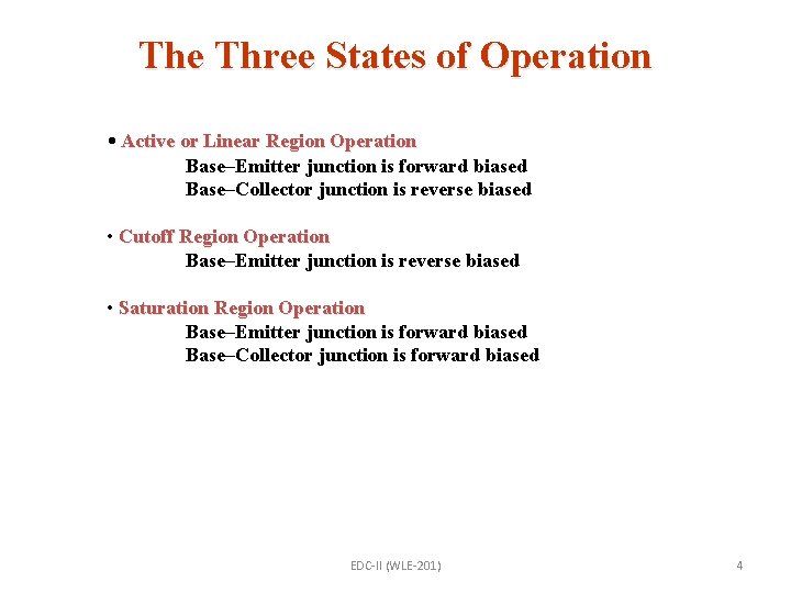
The Three States of Operation • Active or Linear Region Operation Base–Emitter junction is forward biased Base–Collector junction is reverse biased • Cutoff Region Operation Base–Emitter junction is reverse biased • Saturation Region Operation Base–Emitter junction is forward biased Base–Collector junction is forward biased EDC-II (WLE-201) 4

DC Biasing Circuits • • Fixed-bias circuit Emitter-stabilized bias circuit Voltage divider bias circuit DC bias with voltage feedback EDC-II (WLE-201) 5

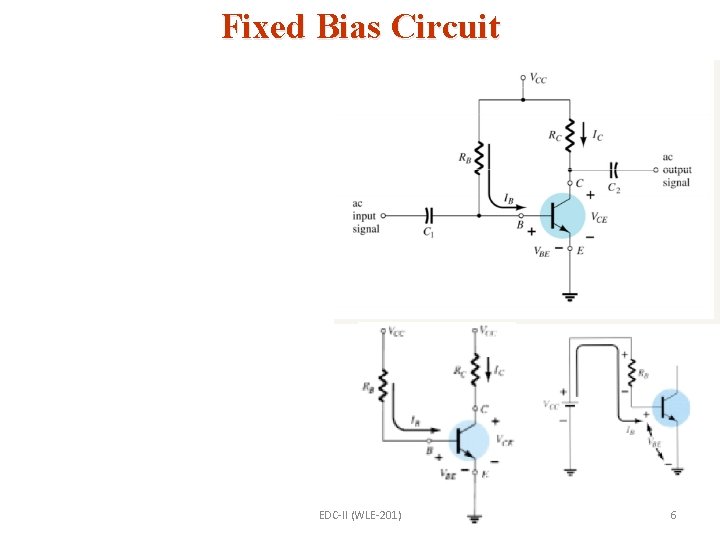
Fixed Bias Circuit EDC-II (WLE-201) 6

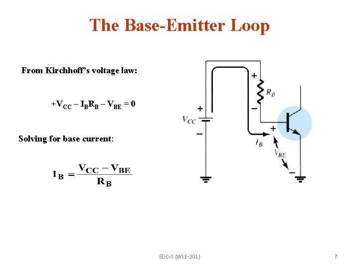
The Base-Emitter Loop From Kirchhoff’s voltage law: +VCC – IBRB – VBE = 0 Solving for base current: EDC-II (WLE-201) 7

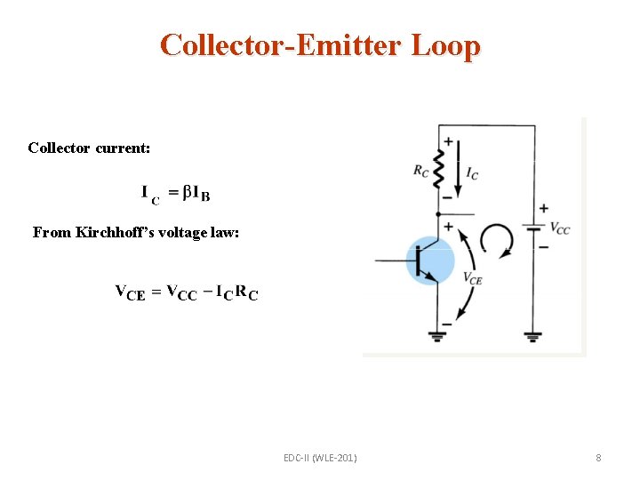
Collector-Emitter Loop Collector current: From Kirchhoff’s voltage law: EDC-II (WLE-201) 8

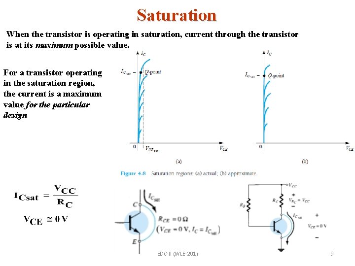
Saturation When the transistor is operating in saturation, current through the transistor is at its maximum possible value. For a transistor operating in the saturation region, the current is a maximum value for the particular design EDC-II (WLE-201) 9

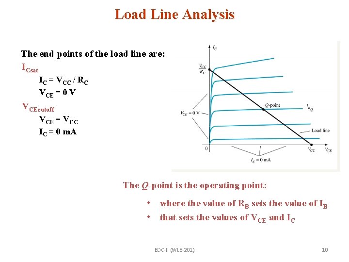
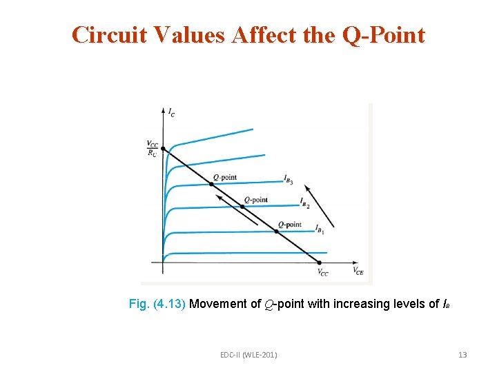
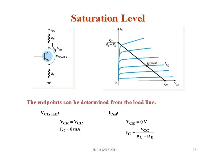
Load Line Analysis The end points of the load line are: ICsat IC = VCC / RC VCE = 0 V VCEcutoff VCE = VCC IC = 0 m. A The Q-point is the operating point: • where the value of RB sets the value of IB • that sets the values of VCE and IC EDC-II (WLE-201) 10

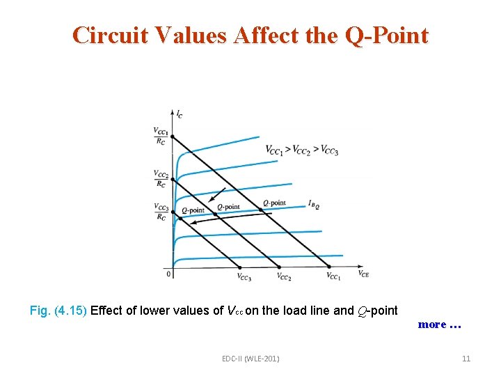
Circuit Values Affect the Q-Point Fig. (4. 15) Effect of lower values of VCC on the load line and Q-point EDC-II (WLE-201) more … 11

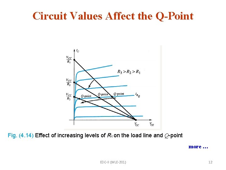
Circuit Values Affect the Q-Point Fig. (4. 14) Effect of increasing levels of RC on the load line and Q-point more … EDC-II (WLE-201) 12

Circuit Values Affect the Q-Point Fig. (4. 13) Movement of Q-point with increasing levels of IB EDC-II (WLE-201) 13

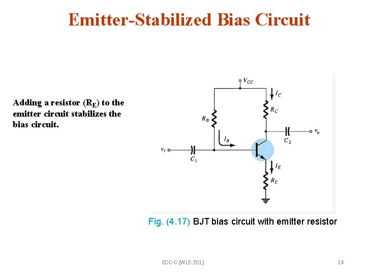
Emitter-Stabilized Bias Circuit Adding a resistor (RE) to the emitter circuit stabilizes the bias circuit. Fig. (4. 17) BJT bias circuit with emitter resistor EDC-II (WLE-201) 14

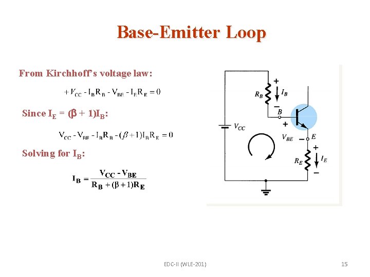
Base-Emitter Loop From Kirchhoff’s voltage law: Since IE = ( + 1)IB: Solving for IB: EDC-II (WLE-201) 15

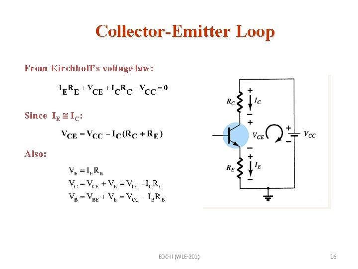
Collector-Emitter Loop From Kirchhoff’s voltage law: Since IE IC: Also: EDC-II (WLE-201) 16

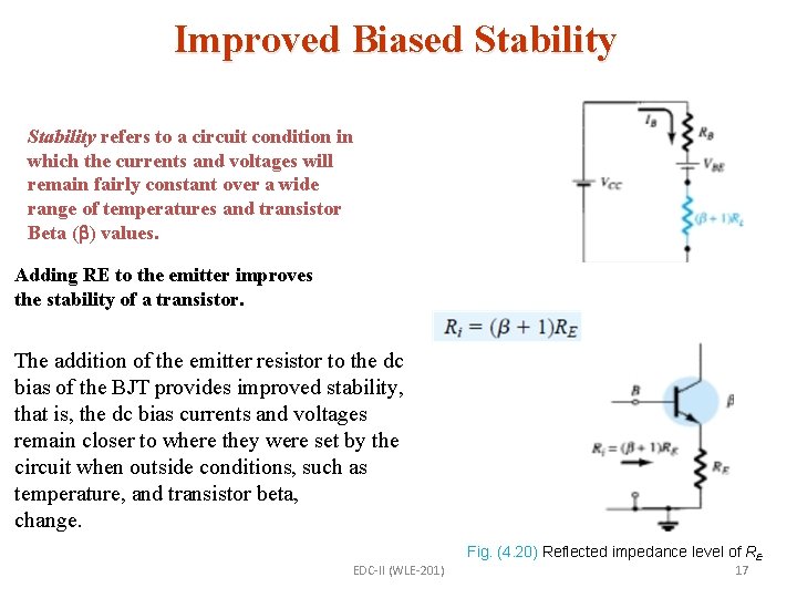
Improved Biased Stability refers to a circuit condition in which the currents and voltages will remain fairly constant over a wide range of temperatures and transistor Beta ( ) values. Adding RE to the emitter improves the stability of a transistor. The addition of the emitter resistor to the dc bias of the BJT provides improved stability, that is, the dc bias currents and voltages remain closer to where they were set by the circuit when outside conditions, such as temperature, and transistor beta, change. EDC-II (WLE-201) Fig. (4. 20) Reflected impedance level of RE 17

Saturation Level The endpoints can be determined from the load line. VCEcutoff: ICsat: EDC-II (WLE-201) 18

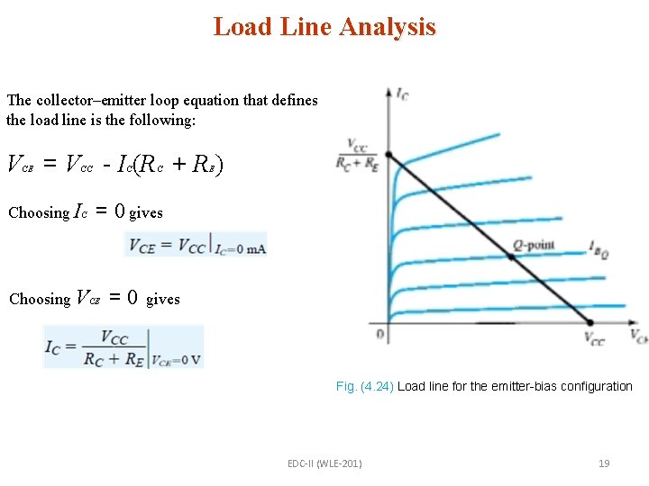
Load Line Analysis The collector–emitter loop equation that defines the load line is the following: V = V - I (R + R ) CE CC Choosing IC C C E = 0 gives Choosing VCE =0 gives Fig. (4. 24) Load line for the emitter-bias configuration EDC-II (WLE-201) 19

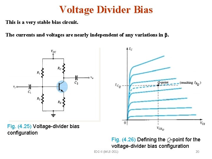
Voltage Divider Bias This is a very stable bias circuit. The currents and voltages are nearly independent of any variations in . Fig. (4. 25) Voltage-divider bias configuration Fig. (4. 26) Defining the Q-point for the voltage-divider bias configuration EDC-II (WLE-201) 20

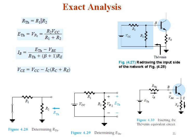
Exact Analysis Fig. (4. 27) Redrawing the input side of the network of Fig. (4. 25) EDC-II (WLE-201) 21

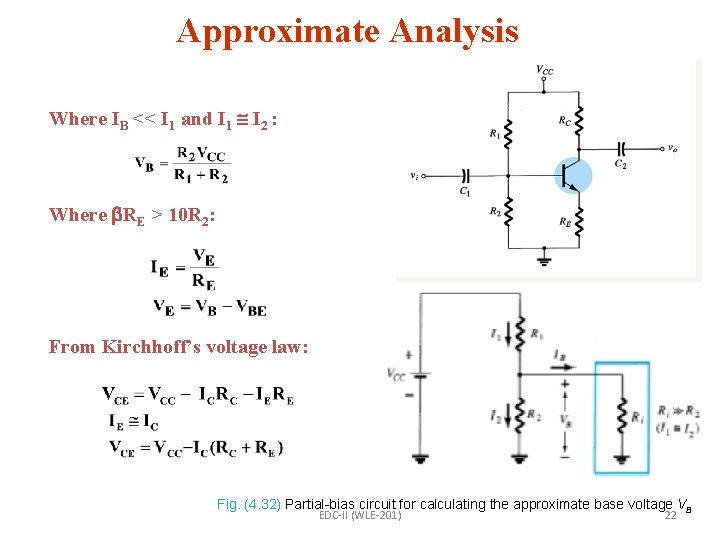
Approximate Analysis Where IB << I 1 and I 1 I 2 : Where RE > 10 R 2: From Kirchhoff’s voltage law: Fig. (4. 32) Partial-bias circuit for calculating the approximate base voltage VB EDC-II (WLE-201) 22

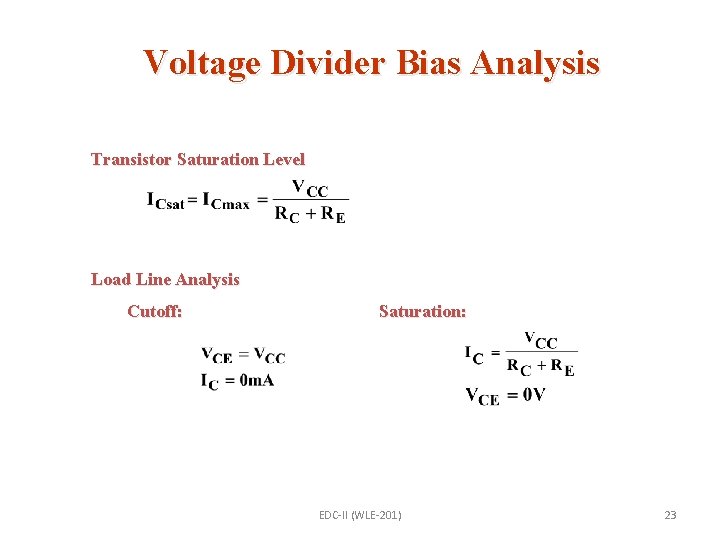
Voltage Divider Bias Analysis Transistor Saturation Level Load Line Analysis Cutoff: Saturation: EDC-II (WLE-201) 23

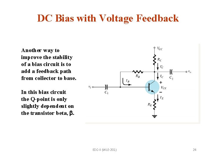
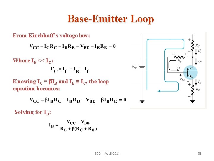
DC Bias with Voltage Feedback Another way to improve the stability of a bias circuit is to add a feedback path from collector to base. In this bias circuit the Q-point is only slightly dependent on the transistor beta, . EDC-II (WLE-201) 24

Base-Emitter Loop From Kirchhoff’s voltage law: Where IB << IC: Knowing IC = IB and IE IC, the loop equation becomes: Solving for IB: EDC-II (WLE-201) 25

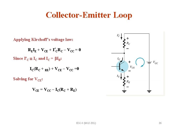
Collector-Emitter Loop Applying Kirchoff’s voltage law: REIE + VCE + I’CRC – VCC = 0 Since I C IC and IC = IB: IC(RC + RE) + VCE – VCC =0 Solving for VCE: VCE = VCC – IC(RC + RE) EDC-II (WLE-201) 26

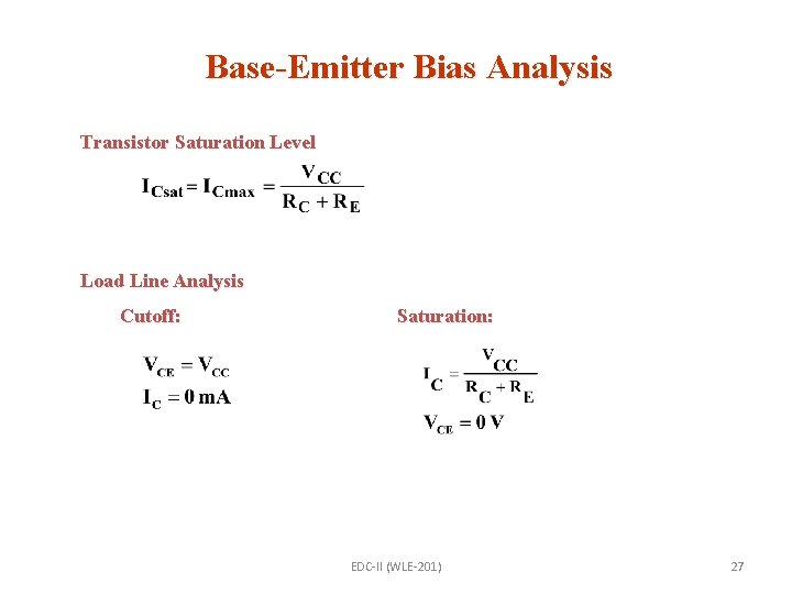
Base-Emitter Bias Analysis Transistor Saturation Level Load Line Analysis Cutoff: Saturation: EDC-II (WLE-201) 27

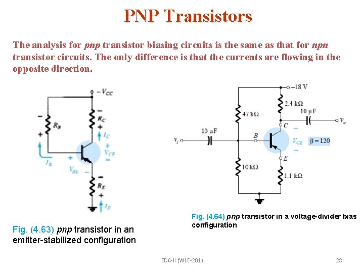
PNP Transistors The analysis for pnp transistor biasing circuits is the same as that for npn transistor circuits. The only difference is that the currents are flowing in the opposite direction. Fig. (4. 63) pnp transistor in an emitter-stabilized configuration Fig. (4. 64) pnp transistor in a voltage-divider bias configuration EDC-II (WLE-201) 28

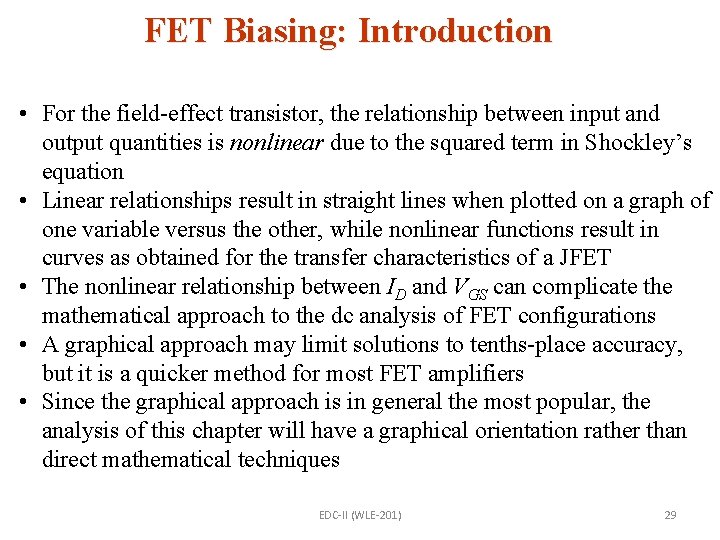
FET Biasing: Introduction • For the field-effect transistor, the relationship between input and output quantities is nonlinear due to the squared term in Shockley’s equation • Linear relationships result in straight lines when plotted on a graph of one variable versus the other, while nonlinear functions result in curves as obtained for the transfer characteristics of a JFET • The nonlinear relationship between ID and VGS can complicate the mathematical approach to the dc analysis of FET configurations • A graphical approach may limit solutions to tenths-place accuracy, but it is a quicker method for most FET amplifiers • Since the graphical approach is in general the most popular, the analysis of this chapter will have a graphical orientation rather than direct mathematical techniques EDC-II (WLE-201) 29

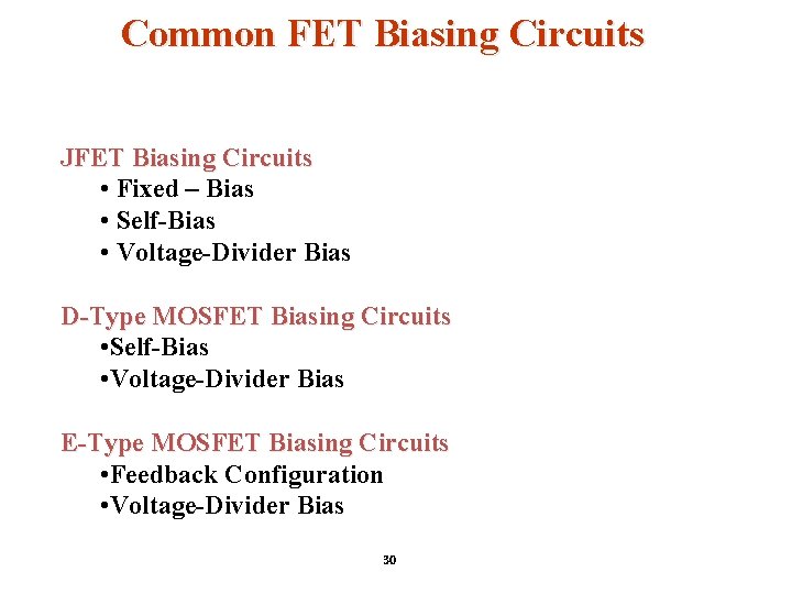
Common FET Biasing Circuits JFET Biasing Circuits • Fixed – Bias • Self-Bias • Voltage-Divider Bias D-Type MOSFET Biasing Circuits • Self-Bias • Voltage-Divider Bias E-Type MOSFET Biasing Circuits • Feedback Configuration • Voltage-Divider Bias 30

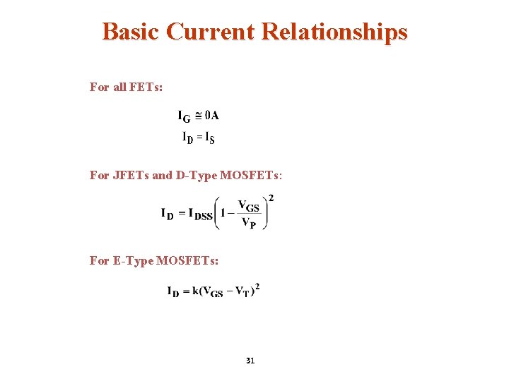
Basic Current Relationships For all FETs: For JFETs and D-Type MOSFETs: For E-Type MOSFETs: 31

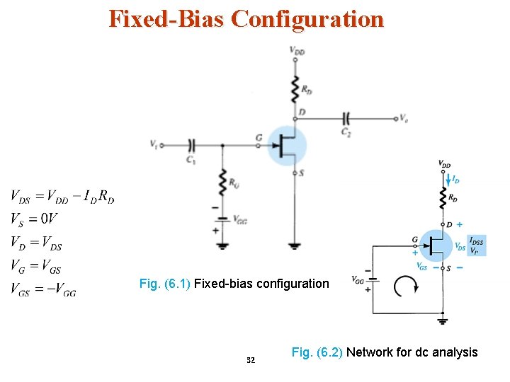
Fixed-Bias Configuration Fig. (6. 1) Fixed-bias configuration 32 Fig. (6. 2) Network for dc analysis

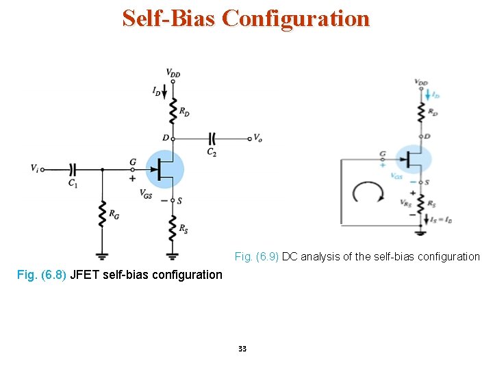
Self-Bias Configuration Fig. (6. 9) DC analysis of the self-bias configuration Fig. (6. 8) JFET self-bias configuration 33

Self-Bias Calculations For the indicated loop, To solve this equation: • Select an ID < IDSS and use the component value of RS to calculate VGS • Plot the point identified by ID and VGS. Draw a line from the origin of the axis to this point. • Plot the transfer curve using IDSS and VP (VP = VGSoff in specification sheets) and a few points such as ID = IDSS / 4 and ID = IDSS / 2 etc. The Q-point is located where the first line intersects the transfer curve. Use the value of ID at the Q-point (IDQ) to solve for the other voltages: 34 Fig. (6. 11) Sketching the self bias line

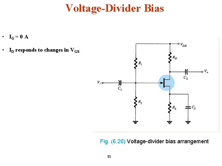
Voltage-Divider Bias • IG = 0 A • ID responds to changes in VGS Fig. (6. 20) Voltage-divider bias arrangement 35

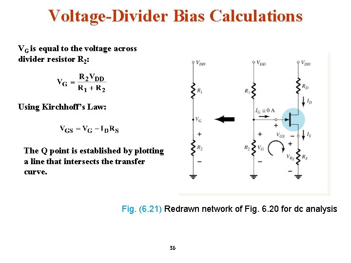
Voltage-Divider Bias Calculations VG is equal to the voltage across divider resistor R 2: Using Kirchhoff’s Law: The Q point is established by plotting a line that intersects the transfer curve. Fig. (6. 21) Redrawn network of Fig. 6. 20 for dc analysis 36

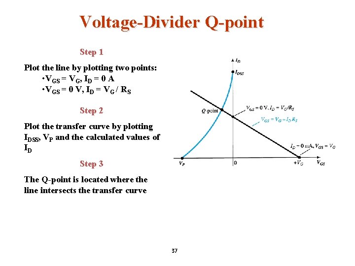
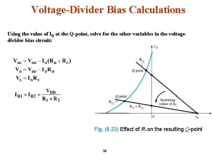
Voltage-Divider Q-point Step 1 Plot the line by plotting two points: • VGS = VG, ID = 0 A • VGS = 0 V, ID = VG / RS Step 2 Plot the transfer curve by plotting IDSS, VP and the calculated values of ID Step 3 The Q-point is located where the line intersects the transfer curve 37

Voltage-Divider Bias Calculations Using the value of ID at the Q-point, solve for the other variables in the voltagedivider bias circuit: Fig. (6. 23) Effect of RS on the resulting Q-point 38

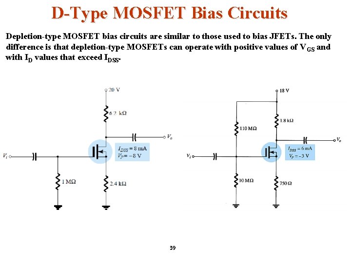
D-Type MOSFET Bias Circuits Depletion-type MOSFET bias circuits are similar to those used to bias JFETs. The only difference is that depletion-type MOSFETs can operate with positive values of VGS and with ID values that exceed IDSS. 39

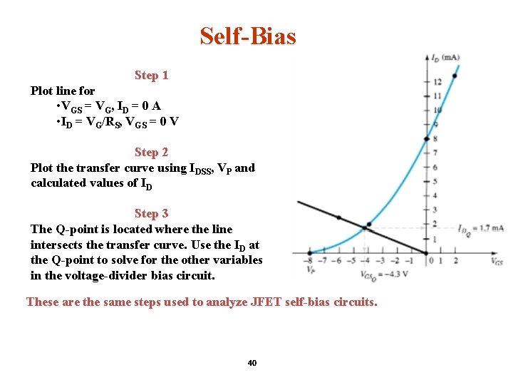
Self-Bias Step 1 Plot line for • VGS = VG, ID = 0 A • ID = VG/RS, VGS = 0 V Step 2 Plot the transfer curve using IDSS, VP and calculated values of ID Step 3 The Q-point is located where the line intersects the transfer curve. Use the ID at the Q-point to solve for the other variables in the voltage-divider bias circuit. These are the same steps used to analyze JFET self-bias circuits. 40

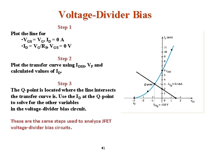
Voltage-Divider Bias Step 1 Plot the line for • VGS = VG, ID = 0 A • ID = VG/RS, VGS = 0 V Step 2 Plot the transfer curve using IDSS, VP and calculated values of ID. Step 3 The Q-point is located where the line intersects the transfer curve is. Use the ID at the Q-point to solve for the other variables in the voltage-divider bias circuit. These are the same steps used to analyze JFET voltage-divider bias circuits. 41

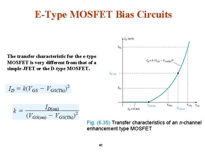
E-Type MOSFET Bias Circuits The transfer characteristic for the e-type MOSFET is very different from that of a simple JFET or the D-type MOSFET. Fig. (6. 35) Transfer characteristics of an n-channel enhancement type MOSFET 42

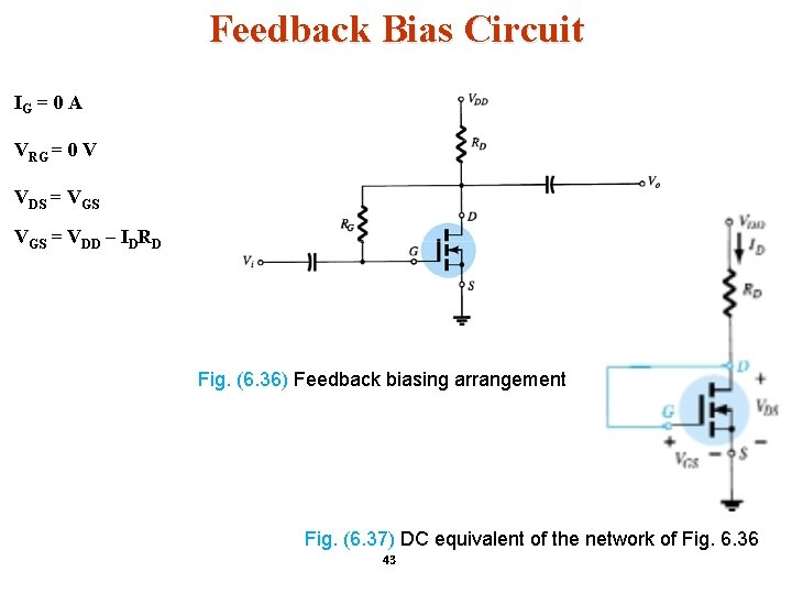
Feedback Bias Circuit IG = 0 A VRG = 0 V VDS = VGS = VDD – IDRD Fig. (6. 36) Feedback biasing arrangement Fig. (6. 37) DC equivalent of the network of Fig. 6. 36 43

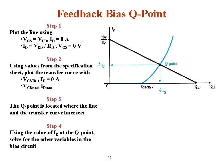
Feedback Bias Q-Point Step 1 Plot the line using • VGS = VDD, ID = 0 A • ID = VDD / RD , VGS = 0 V Step 2 Using values from the specification sheet, plot the transfer curve with • VGSTh , ID = 0 A • VGS(on), ID(on) Step 3 The Q-point is located where the line and the transfer curve intersect Step 4 Using the value of ID at the Q-point, solve for the other variables in the bias circuit 44

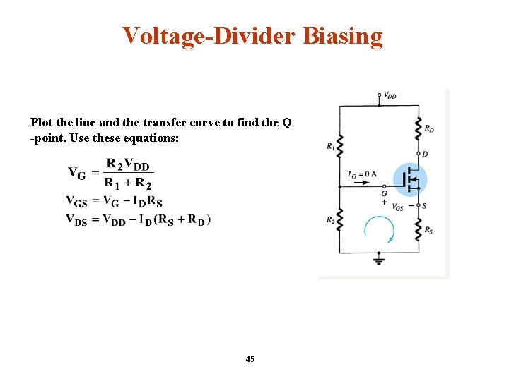
Voltage-Divider Biasing Plot the line and the transfer curve to find the Q -point. Use these equations: 45

Voltage-Divider Bias Q-Point Step 1 Plot the line using • VGS = VG = (R 2 VDD) / (R 1 + R 2), ID = 0 A • ID = VG/RS , VGS = 0 V Step 2 Using values from the specification sheet, plot the transfer curve with • VGSTh, ID = 0 A • VGS(on) , ID(on) Step 3 The point where the line and the transfer curve intersect is the Qpoint. Step 4 Using the value of ID at the Q-point, solve for the other circuit values. 46

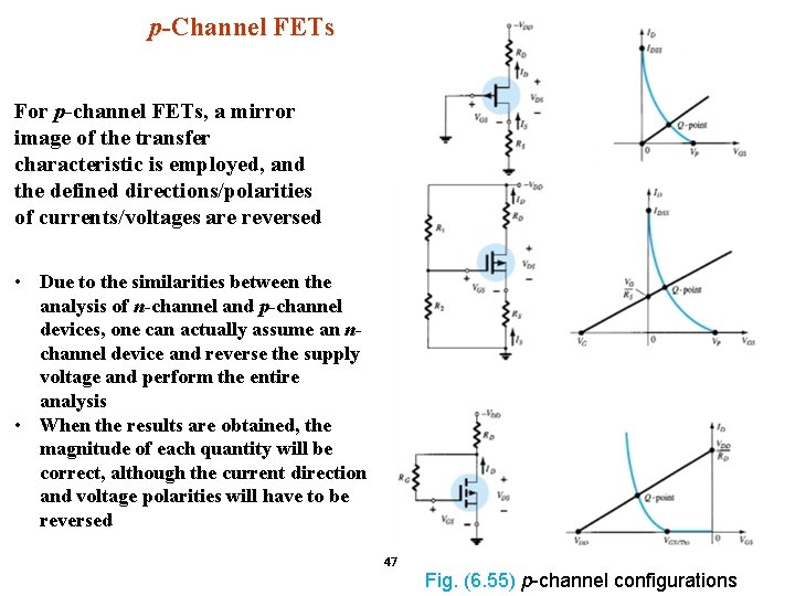
p-Channel FETs For p-channel FETs, a mirror image of the transfer characteristic is employed, and the defined directions/polarities of currents/voltages are reversed • Due to the similarities between the analysis of n-channel and p-channel devices, one can actually assume an nchannel device and reverse the supply voltage and perform the entire analysis • When the results are obtained, the magnitude of each quantity will be correct, although the current direction and voltage polarities will have to be reversed 47 Fig. (6. 55) p-channel configurations

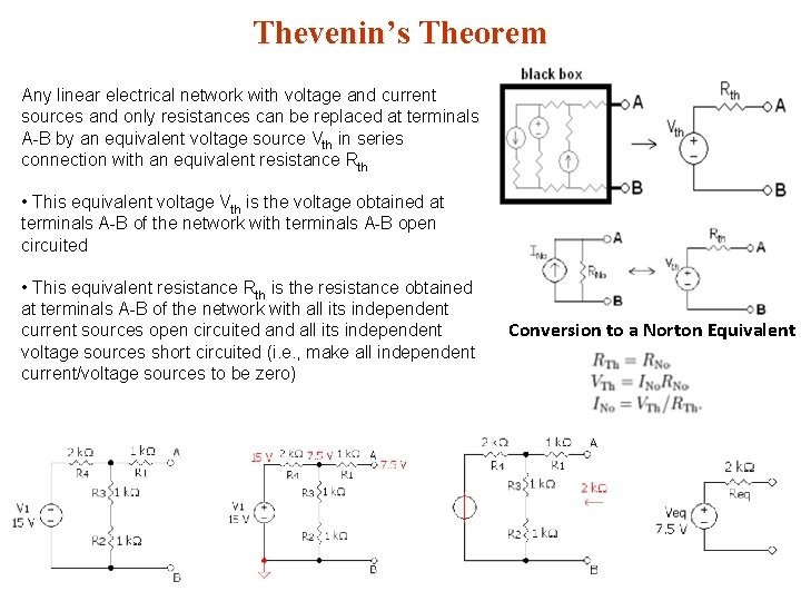
Thevenin’s Theorem Any linear electrical network with voltage and current sources and only resistances can be replaced at terminals A-B by an equivalent voltage source Vth in series connection with an equivalent resistance Rth • This equivalent voltage Vth is the voltage obtained at terminals A-B of the network with terminals A-B open circuited • This equivalent resistance Rth is the resistance obtained at terminals A-B of the network with all its independent current sources open circuited and all its independent voltage sources short circuited (i. e. , make all independent current/voltage sources to be zero) Conversion to a Norton Equivalent