Universidade Federal de Santa Catarina Centro Tecnolgico Computer
![Combinational Circuits in CMOS O Comportamento do Transistor de Passagem 3. 0 Tensão [V] Combinational Circuits in CMOS O Comportamento do Transistor de Passagem 3. 0 Tensão [V]](https://slidetodoc.com/presentation_image/2f1d14100b54c4856e5e455d970a8ba2/image-50.jpg)
![Combinational Circuits in CMOS Restorer Sizing Voltage [V] 3. 0 2. 0 • Upper Combinational Circuits in CMOS Restorer Sizing Voltage [V] 3. 0 2. 0 • Upper](https://slidetodoc.com/presentation_image/2f1d14100b54c4856e5e455d970a8ba2/image-53.jpg)
- Slides: 62

Universidade Federal de Santa Catarina Centro Tecnológico Computer Science & Electrical Engineering Digital Integrated Circuits INE 5442 / EEL 7312 Lectures 33 to 36 Combinational Circuits in CMOS Prof. José Luís Güntzel guntzel@inf. ufsc. br INE 5442 / EEL 7312 Digital Integrated Circuits 1

Combinational Circuits in CMOS Agenda • • Complementary CMOS Pass-Transistor Logic INE 5442 / EEL 7312 Digital Integrated Circuits 2 Lectures 33 to 36 Prof. Güntzel

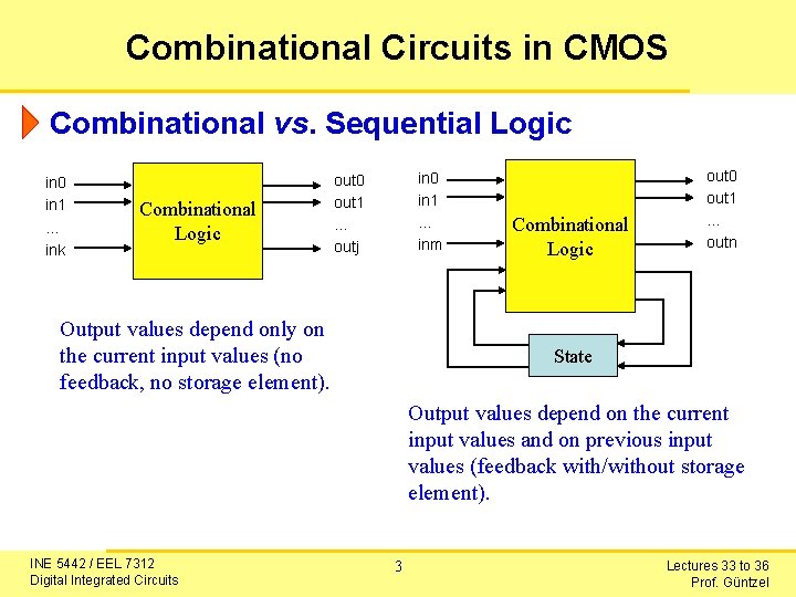
Combinational Circuits in CMOS Combinational vs. Sequential Logic in 0 in 1. . . ink Combinational Logic in 0 in 1. . . inm out 0 out 1. . . outj Output values depend only on the current input values (no feedback, no storage element). Combinational Logic out 0 out 1. . . outn State Output values depend on the current input values and on previous input values (feedback with/without storage element). INE 5442 / EEL 7312 Digital Integrated Circuits 3 Lectures 33 to 36 Prof. Güntzel

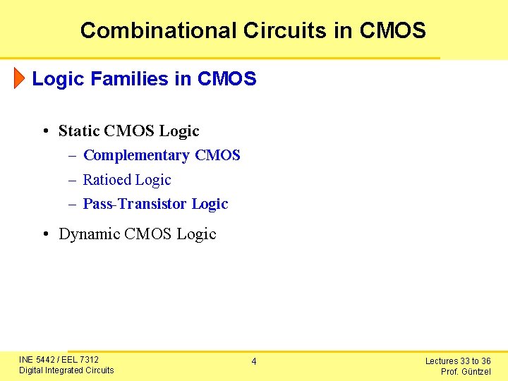
Combinational Circuits in CMOS Logic Families in CMOS • Static CMOS Logic – Complementary CMOS – Ratioed Logic – Pass-Transistor Logic • Dynamic CMOS Logic INE 5442 / EEL 7312 Digital Integrated Circuits 4 Lectures 33 to 36 Prof. Güntzel

Combinational Circuits in CMOS Metrics for Choosing a Gate Design/Family • Area in silicon (related to number of transistors) • Speed (propagation delay) • Energy consumption/Power dissipation • Robustness to noise • Reliability • Manufacturability “Depending on the application, the emphasis will be on different metrics. ” (Rabaey; Chandrakasan; Nikolic, 2005) INE 5442 / EEL 7312 Digital Integrated Circuits 5 Lectures 33 to 36 Prof. Güntzel

Combinational Circuits in CMOS Static CMOS Logic Features: • Robustness (low sensitivity to noise). • Good performance. • Low power consumption (no static consumption, except for leakage currents). • Easy to design (good for novice designers…) INE 5442 / EEL 7312 Digital Integrated Circuits 6 Lectures 33 to 36 Prof. Güntzel

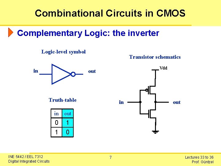
Combinational Circuits in CMOS Complementary Logic: the inverter Logic-level symbol in Transistor schematics Vdd out Truth-table in out INE 5442 / EEL 7312 Digital Integrated Circuits 0 1 1 0 7 Lectures 33 to 36 Prof. Güntzel

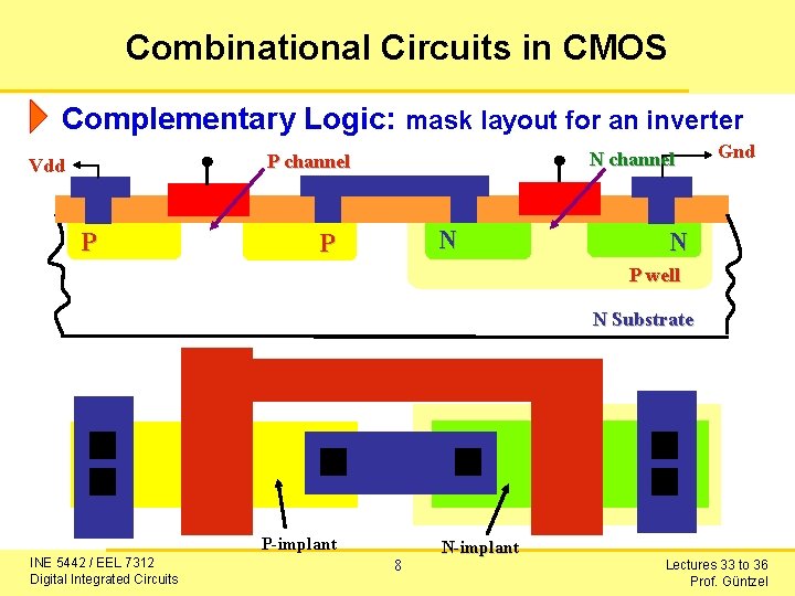
Combinational Circuits in CMOS Complementary Logic: mask layout for an inverter N channel P channel Vdd P N P Gnd N P well N Substrate P-implant INE 5442 / EEL 7312 Digital Integrated Circuits 8 N-implant Lectures 33 to 36 Prof. Güntzel

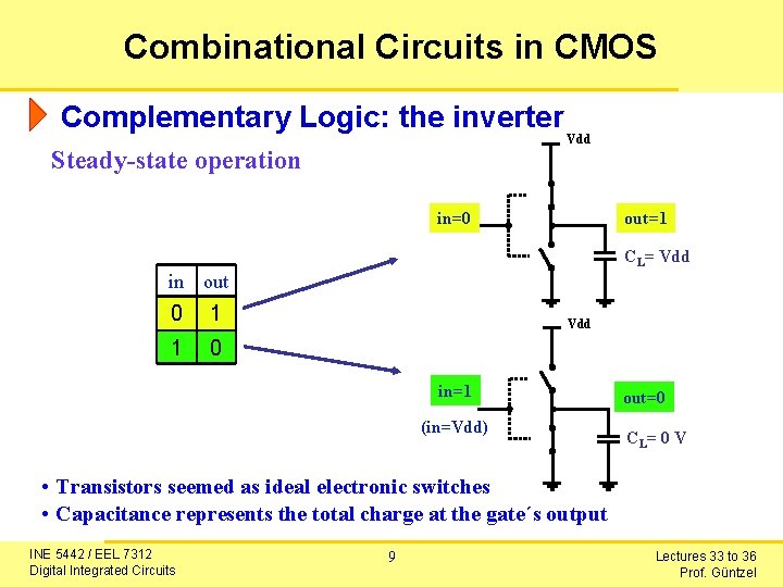
Combinational Circuits in CMOS Complementary Logic: the inverter Steady-state operation Vdd in=0 out=1 CL= Vdd in out 0 1 1 0 Vdd in=1 (in=Vdd) out=0 CL= 0 V • Transistors seemed as ideal electronic switches • Capacitance represents the total charge at the gate´s output INE 5442 / EEL 7312 Digital Integrated Circuits 9 Lectures 33 to 36 Prof. Güntzel

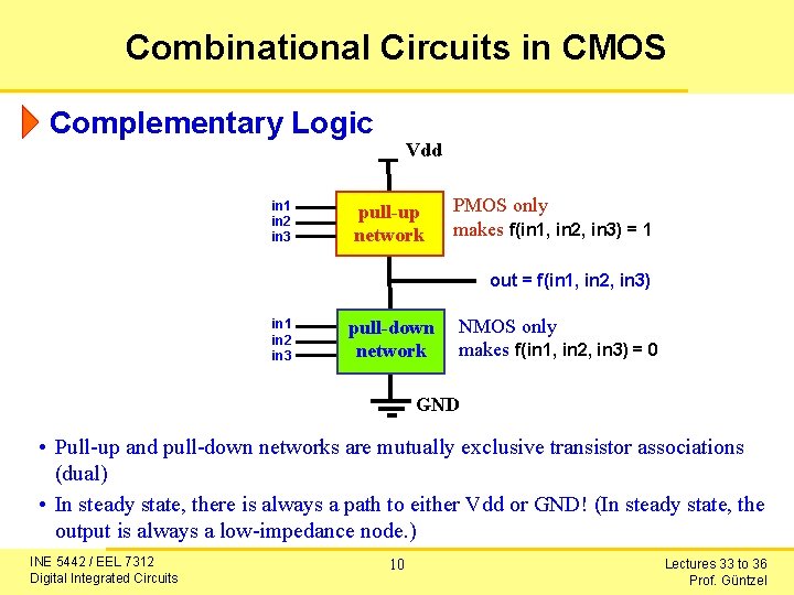
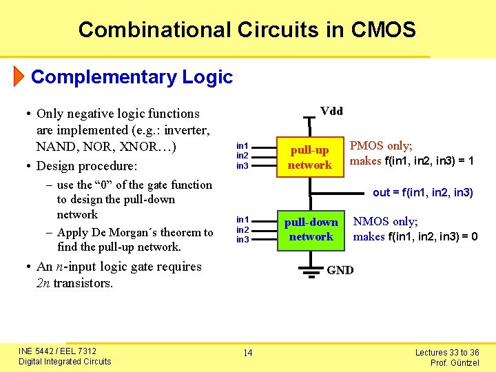
Combinational Circuits in CMOS Complementary Logic in 1 in 2 in 3 Vdd pull-up network PMOS only makes f(in 1, in 2, in 3) = 1 out = f(in 1, in 2, in 3) in 1 in 2 in 3 pull-down network NMOS only makes f(in 1, in 2, in 3) = 0 GND • Pull-up and pull-down networks are mutually exclusive transistor associations (dual) • In steady state, there is always a path to either Vdd or GND! (In steady state, the output is always a low-impedance node. ) INE 5442 / EEL 7312 Digital Integrated Circuits 10 Lectures 33 to 36 Prof. Güntzel

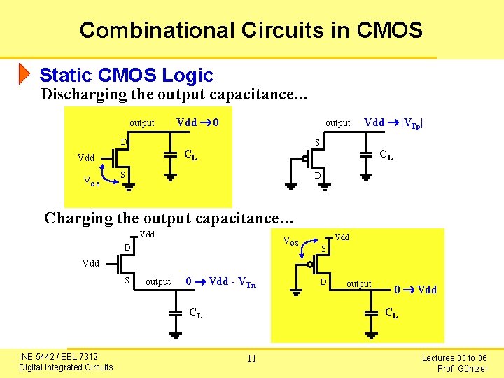
Combinational Circuits in CMOS Static CMOS Logic Discharging the output capacitance… output Vdd 0 output D S CL Vdd VGS Vdd |VTp| CL S D Charging the output capacitance… Vdd VGS D Vdd S output 0 Vdd - VTn CL INE 5442 / EEL 7312 Digital Integrated Circuits D output 0 Vdd CL 11 Lectures 33 to 36 Prof. Güntzel

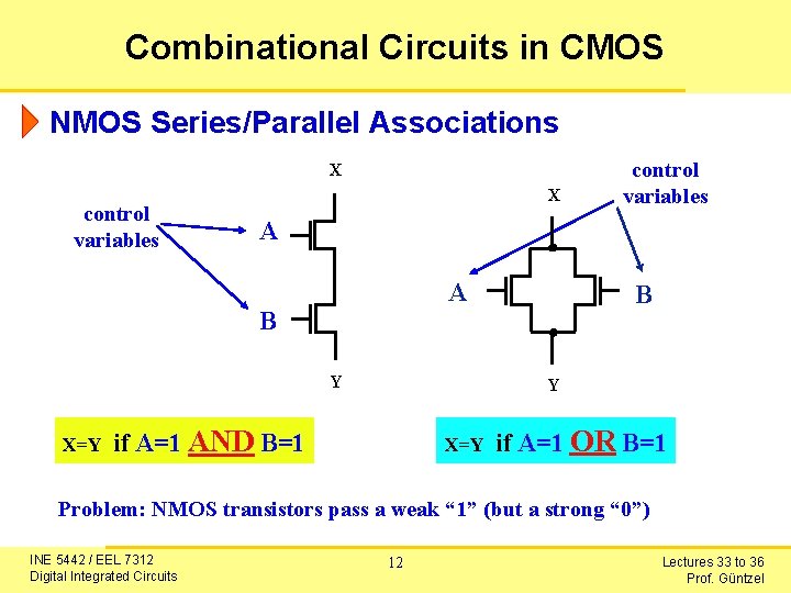
Combinational Circuits in CMOS NMOS Series/Parallel Associations X control variables X A A B Y X=Y control variables B Y if A=1 AND B=1 X=Y if A=1 OR B=1 Problem: NMOS transistors pass a weak “ 1” (but a strong “ 0”) INE 5442 / EEL 7312 Digital Integrated Circuits 12 Lectures 33 to 36 Prof. Güntzel

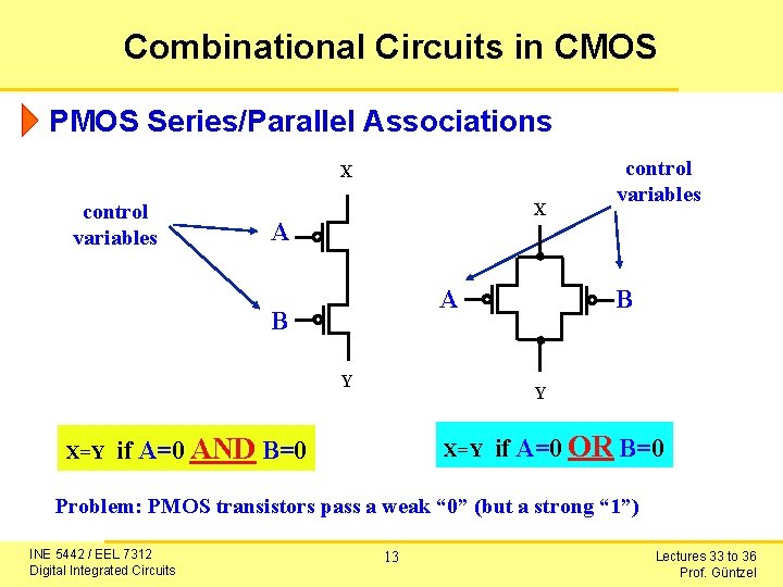
Combinational Circuits in CMOS PMOS Series/Parallel Associations X control variables X A A B Y X=Y control variables B Y if A=0 AND B=0 X=Y if A=0 OR B=0 Problem: PMOS transistors pass a weak “ 0” (but a strong “ 1”) INE 5442 / EEL 7312 Digital Integrated Circuits 13 Lectures 33 to 36 Prof. Güntzel

Combinational Circuits in CMOS Complementary Logic • Only negative logic functions are implemented (e. g. : inverter, NAND, NOR, XNOR…) • Design procedure: – use the “ 0” of the gate function to design the pull-down network – Apply De Morgan´s theorem to find the pull-up network. Vdd in 1 in 2 in 3 PMOS only; makes f(in 1, in 2, in 3) = 1 out = f(in 1, in 2, in 3) in 1 in 2 in 3 • An n-input logic gate requires 2 n transistors. INE 5442 / EEL 7312 Digital Integrated Circuits pull-up network pull-down network NMOS only; makes f(in 1, in 2, in 3) = 0 GND 14 Lectures 33 to 36 Prof. Güntzel

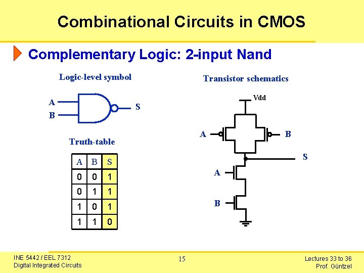
Combinational Circuits in CMOS Complementary Logic: 2 -input Nand Logic-level symbol A B Transistor schematics Vdd S Truth-table A B S 0 0 1 1 1 0 INE 5442 / EEL 7312 Digital Integrated Circuits B A S A B 15 Lectures 33 to 36 Prof. Güntzel

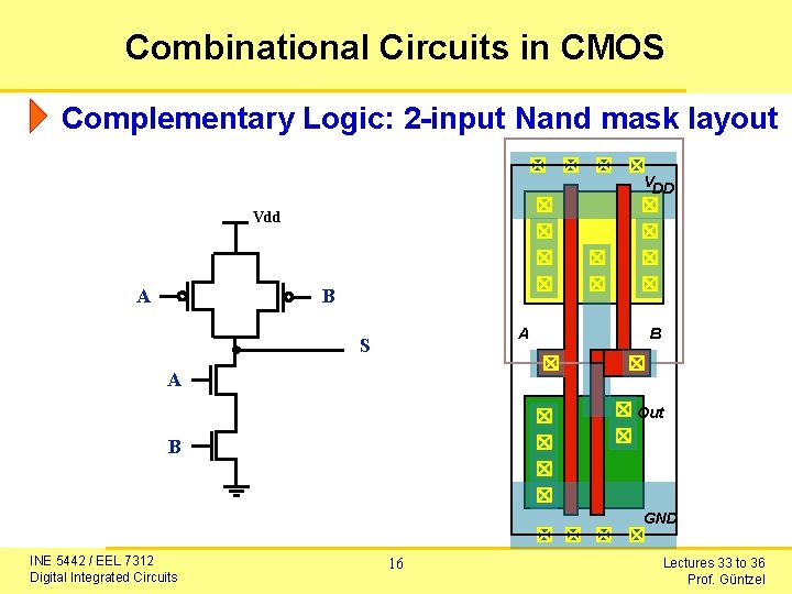
Combinational Circuits in CMOS Complementary Logic: 2 -input Nand mask layout VDD Vdd B A A S B A Out B GND INE 5442 / EEL 7312 Digital Integrated Circuits 16 Lectures 33 to 36 Prof. Güntzel

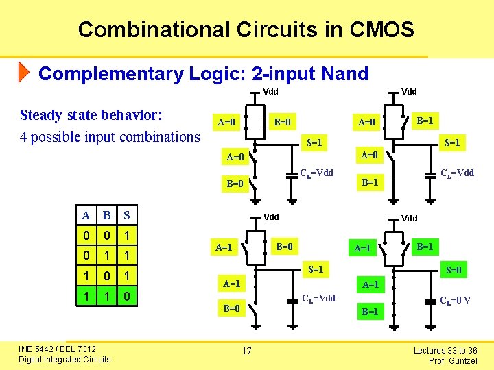
Combinational Circuits in CMOS Complementary Logic: 2 -input Nand Vdd Steady state behavior: 4 possible input combinations Vdd B=0 A=0 S=1 CL=Vdd B=0 S 0 0 1 1 1 0 INE 5442 / EEL 7312 Digital Integrated Circuits S=1 A=0 A B B=1 Vdd B=0 A=1 CL=Vdd B=1 A=1 S=1 A=1 B=1 S=0 A=1 CL=Vdd B=0 B=1 17 CL=0 V Lectures 33 to 36 Prof. Güntzel

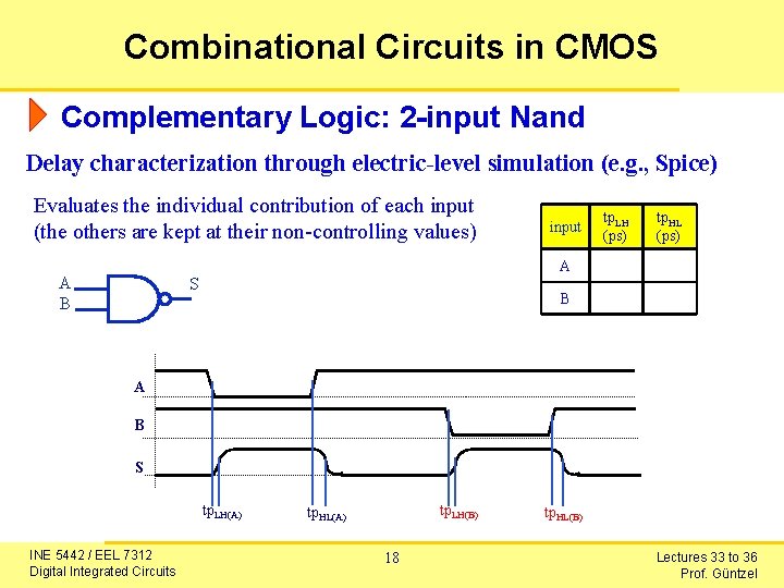
Combinational Circuits in CMOS Complementary Logic: 2 -input Nand Delay characterization through electric-level simulation (e. g. , Spice) Evaluates the individual contribution of each input (the others are kept at their non-controlling values) A B input tp. LH (ps) tp. HL (ps) A S B A B S tp. LH(A) INE 5442 / EEL 7312 Digital Integrated Circuits tp. LH(B) tp. HL(A) 18 tp. HL(B) Lectures 33 to 36 Prof. Güntzel

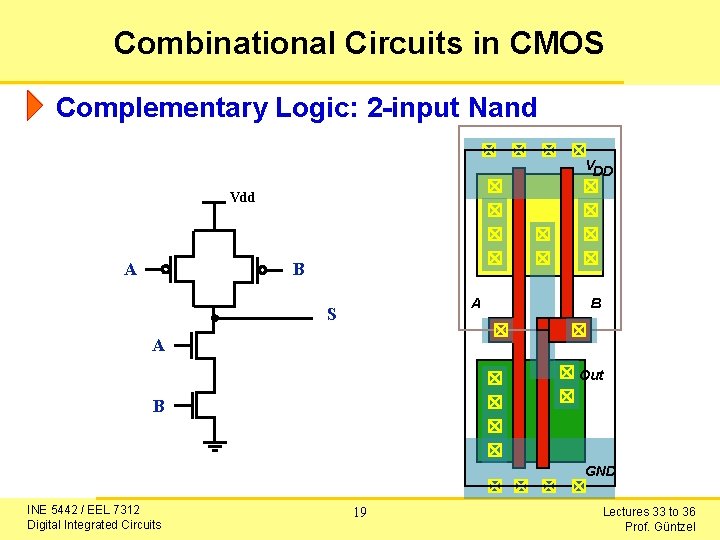
Combinational Circuits in CMOS Complementary Logic: 2 -input Nand VDD Vdd B A A S B A Out B GND INE 5442 / EEL 7312 Digital Integrated Circuits 19 Lectures 33 to 36 Prof. Güntzel

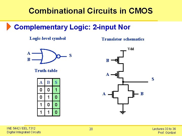
Combinational Circuits in CMOS Complementary Logic: 2 -input Nor Logic-level symbol Transistor schematics Vdd A B S B Truth-table A B S 0 0 1 0 1 0 0 1 1 0 INE 5442 / EEL 7312 Digital Integrated Circuits A A 20 S B Lectures 33 to 36 Prof. Güntzel

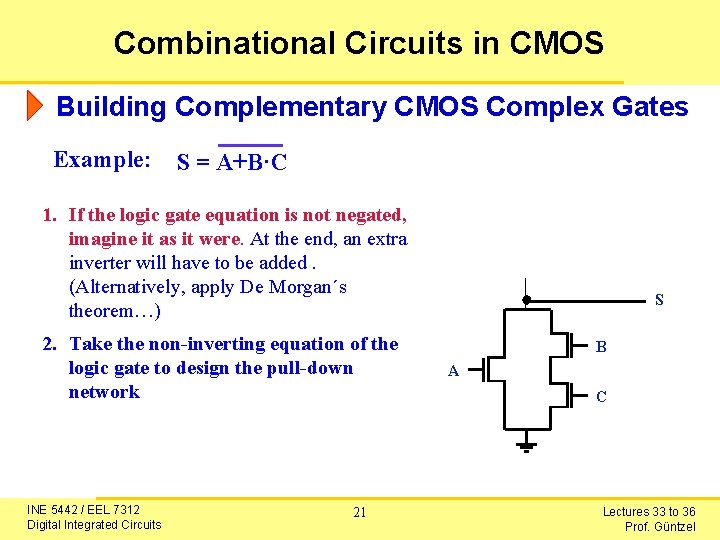
Combinational Circuits in CMOS Building Complementary CMOS Complex Gates Example: S = A+B·C 1. If the logic gate equation is not negated, imagine it as it were. At the end, an extra inverter will have to be added. (Alternatively, apply De Morgan´s theorem…) 2. Take the non-inverting equation of the logic gate to design the pull-down network INE 5442 / EEL 7312 Digital Integrated Circuits 21 S B A C Lectures 33 to 36 Prof. Güntzel

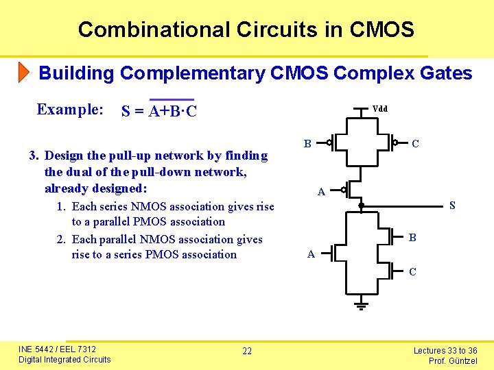
Combinational Circuits in CMOS Building Complementary CMOS Complex Gates Example: S = A+B·C Vdd 3. Design the pull-up network by finding the dual of the pull-down network, already designed: 1. Each series NMOS association gives rise to a parallel PMOS association 2. Each parallel NMOS association gives rise to a series PMOS association B C A S B A C INE 5442 / EEL 7312 Digital Integrated Circuits 22 Lectures 33 to 36 Prof. Güntzel

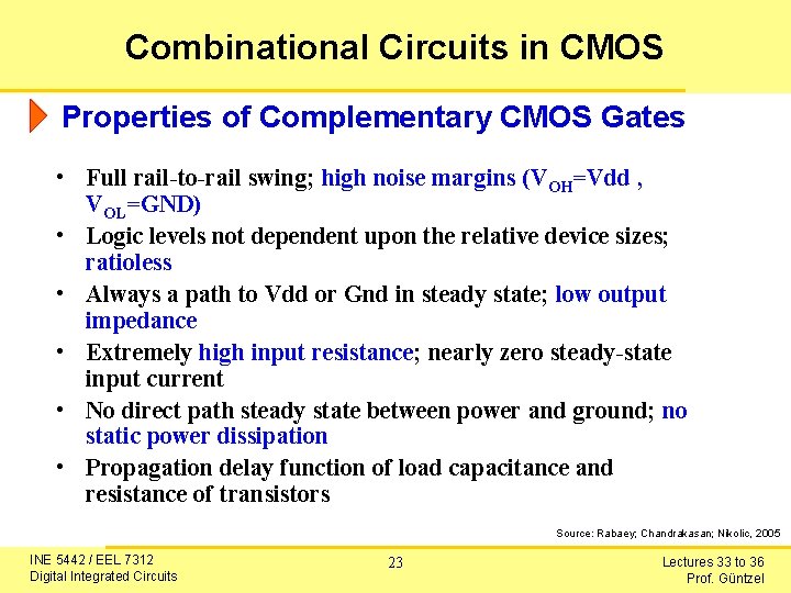
Combinational Circuits in CMOS Properties of Complementary CMOS Gates • Full rail-to-rail swing; high noise margins (VOH=Vdd , VOL=GND) • Logic levels not dependent upon the relative device sizes; ratioless • Always a path to Vdd or Gnd in steady state; low output impedance • Extremely high input resistance; nearly zero steady-state input current • No direct path steady state between power and ground; no static power dissipation • Propagation delay function of load capacitance and resistance of transistors Source: Rabaey; Chandrakasan; Nikolic, 2005 INE 5442 / EEL 7312 Digital Integrated Circuits 23 Lectures 33 to 36 Prof. Güntzel

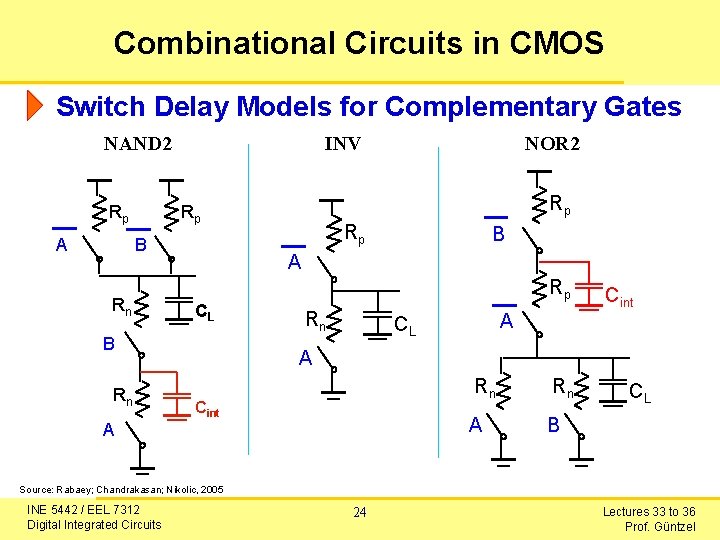
Combinational Circuits in CMOS Switch Delay Models for Complementary Gates NAND 2 Rp A INV Rp Rp B Rn Rp B A CL B Rn NOR 2 Rp Rn A CL Cint A Rn Rn A B CL Source: Rabaey; Chandrakasan; Nikolic, 2005 INE 5442 / EEL 7312 Digital Integrated Circuits 24 Lectures 33 to 36 Prof. Güntzel

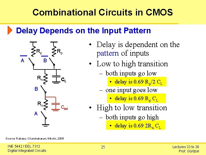
Combinational Circuits in CMOS Delay Depends on the Input Pattern Rp A Rp B Rn CL – both inputs go low • delay is 0. 69 Rp/2 CL – one input goes low B Rn • Delay is dependent on the pattern of inputs • Low to high transition • delay is 0. 69 Rp CL Cint A • High to low transition – both inputs go high • delay is 0. 69 2 Rn CL Source: Rabaey; Chandrakasan; Nikolic, 2005 INE 5442 / EEL 7312 Digital Integrated Circuits 25 Lectures 33 to 36 Prof. Güntzel

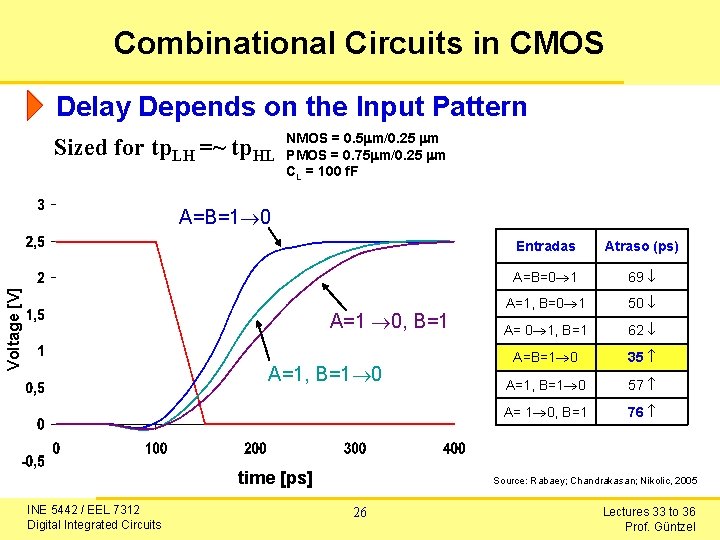
Combinational Circuits in CMOS Delay Depends on the Input Pattern Sized for tp. LH =~ tp. HL NMOS = 0. 5 m/0. 25 m PMOS = 0. 75 m/0. 25 m CL = 100 f. F Voltage [V] A=B=1 0 A=1 0, B=1 A=1, B=1 0 time [ps] INE 5442 / EEL 7312 Digital Integrated Circuits Entradas Atraso (ps) A=B=0 1 69 A=1, B=0 1 50 A= 0 1, B=1 62 A=B=1 0 35 A=1, B=1 0 57 A= 1 0, B=1 76 Source: Rabaey; Chandrakasan; Nikolic, 2005 26 Lectures 33 to 36 Prof. Güntzel

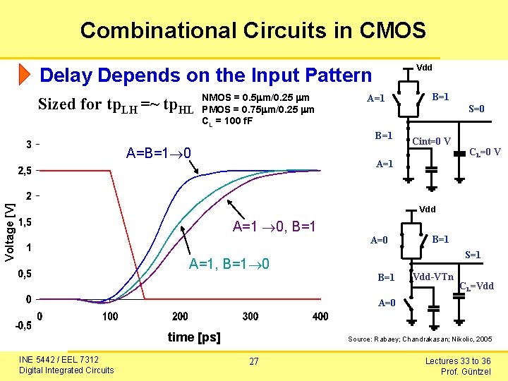
Combinational Circuits in CMOS Vdd Delay Depends on the Input Pattern Sized for tp. LH =~ tp. HL NMOS = 0. 5 m/0. 25 m PMOS = 0. 75 m/0. 25 m CL = 100 f. F A=1 S=0 B=1 Voltage [V] A=B=1 0 B=1 Cint=0 V A=1 CL=0 V Vdd A=1 0, B=1 A=0 B=1 S=1 A=1, B=1 0 B=1 Vdd-VTn CL=Vdd A=0 time [ps] INE 5442 / EEL 7312 Digital Integrated Circuits Source: Rabaey; Chandrakasan; Nikolic, 2005 27 Lectures 33 to 36 Prof. Güntzel

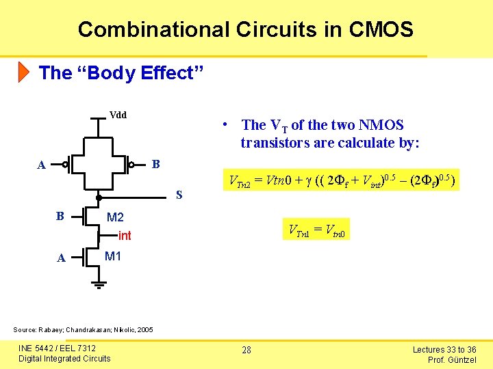
Combinational Circuits in CMOS The “Body Effect” Vdd • The VT of the two NMOS transistors are calculate by: B A S B M 2 int A M 1 VTn 2 = Vtn 0 + (( 2 f + Vint)0. 5 – (2 f)0. 5) VTn 1 = Vtn 0 Source: Rabaey; Chandrakasan; Nikolic, 2005 INE 5442 / EEL 7312 Digital Integrated Circuits 28 Lectures 33 to 36 Prof. Güntzel

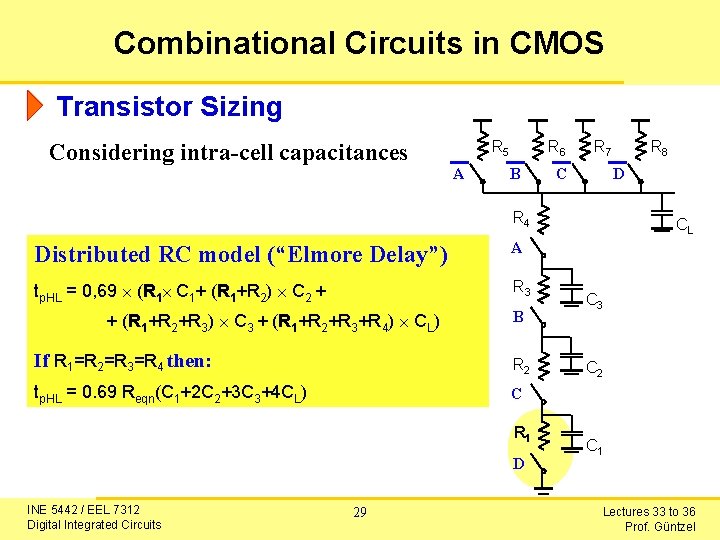
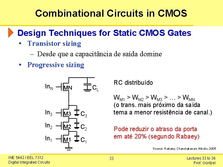
Combinational Circuits in CMOS Transistor Sizing Considering intra-cell capacitances R 5 A R 6 B R 7 C D R 4 Distributed RC model (“Elmore Delay”) A tp. HL = 0, 69 (R 1 C 1+ (R 1+R 2) C 2 + R 3 + (R 1+R 2+R 3) C 3 + (R 1+R 2+R 3+R 4) CL) B If R 1=R 2=R 3=R 4 then: R 2 tp. HL = 0. 69 Reqn(C 1+2 C 2+3 C 3+4 CL) C R 1 D INE 5442 / EEL 7312 Digital Integrated Circuits 29 R 8 CL C 3 C 2 C 1 Lectures 33 to 36 Prof. Güntzel

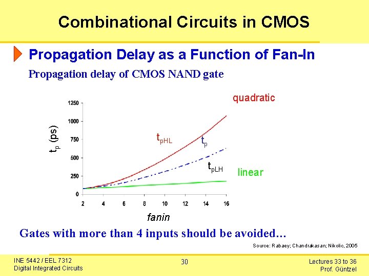
Combinational Circuits in CMOS Propagation Delay as a Function of Fan-In Propagation delay of CMOS NAND gate tp (ps) quadratic tp. HL tp tp. LH linear fanin Gates with more than 4 inputs should be avoided… Source: Rabaey; Chandrakasan; Nikolic, 2005 INE 5442 / EEL 7312 Digital Integrated Circuits 30 Lectures 33 to 36 Prof. Güntzel

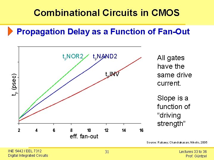
Combinational Circuits in CMOS Propagation Delay as a Function of Fan-Out tp. NOR 2 tp. NAND 2 tp (psec) tp. INV All gates have the same drive current. Slope is a function of “driving strength” eff. fan-out Source: Rabaey; Chandrakasan; Nikolic, 2005 INE 5442 / EEL 7312 Digital Integrated Circuits 31 Lectures 33 to 36 Prof. Güntzel

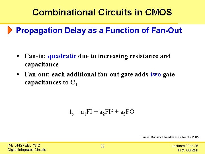
Combinational Circuits in CMOS Propagation Delay as a Function of Fan-Out • Fan-in: quadratic due to increasing resistance and capacitance • Fan-out: each additional fan-out gate adds two gate capacitances to CL tp = a 1 FI + a 2 FI 2 + a 3 FO Source: Rabaey; Chandrakasan; Nikolic, 2005 INE 5442 / EEL 7312 Digital Integrated Circuits 32 Lectures 33 to 36 Prof. Güntzel

Combinational Circuits in CMOS Design Techniques for Static CMOS Gates • Transistor sizing – Desde que a capacitância de saída domine • Progressive sizing In. N RC distribuído CL MN In 3 M 3 C 3 In 2 M 2 C 2 In 1 M 1 C 1 WM 1 > WM 2 > WM 3 > … > WMN (o trans. mais próximo da saída tema a menor resistência de canal. ) Pode reduzir o atraso da porta em até 20% (segundo Rabaey) Source: Rabaey; Chandrakasan; Nikolic, 2005 INE 5442 / EEL 7312 Digital Integrated Circuits 33 Lectures 33 to 36 Prof. Güntzel

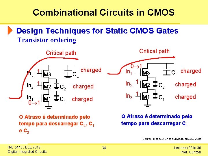
Combinational Circuits in CMOS Design Techniques for Static CMOS Gates Transistor ordering Critical path In 3 1 M 3 In 2 1 M 2 In 1 M 1 0 1 CL 0 1 charged In 1 CL charged M 3 C 2 charged In 2 1 M 2 C 1 charged In 3 1 M 1 C 2 charged C 1 charged O Atraso é determinado pelo tempo para descarregar CL, C 1 e C 2 Source: Rabaey; Chandrakasan; Nikolic, 2005 INE 5442 / EEL 7312 Digital Integrated Circuits 34 Lectures 33 to 36 Prof. Güntzel

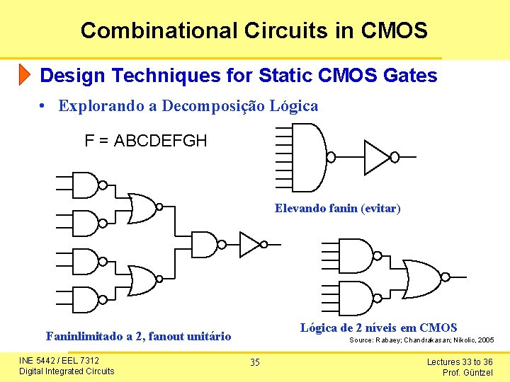
Combinational Circuits in CMOS Design Techniques for Static CMOS Gates • Explorando a Decomposição Lógica F = ABCDEFGH Elevando fanin (evitar) Lógica de 2 níveis em CMOS Faninlimitado a 2, fanout unitário INE 5442 / EEL 7312 Digital Integrated Circuits Source: Rabaey; Chandrakasan; Nikolic, 2005 35 Lectures 33 to 36 Prof. Güntzel

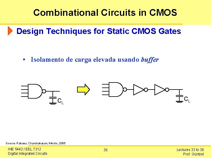
Combinational Circuits in CMOS Design Techniques for Static CMOS Gates • Isolamento de carga elevada usando buffer CL CL Source: Rabaey; Chandrakasan; Nikolic, 2005 INE 5442 / EEL 7312 Digital Integrated Circuits 36 Lectures 33 to 36 Prof. Güntzel

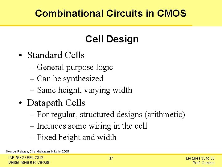
Combinational Circuits in CMOS Cell Design • Standard Cells – General purpose logic – Can be synthesized – Same height, varying width • Datapath Cells – For regular, structured designs (arithmetic) – Includes some wiring in the cell – Fixed height and width Source: Rabaey; Chandrakasan; Nikolic, 2005 INE 5442 / EEL 7312 Digital Integrated Circuits 37 Lectures 33 to 36 Prof. Güntzel

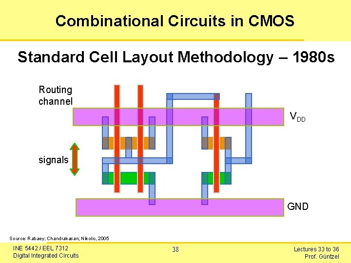
Combinational Circuits in CMOS Standard Cell Layout Methodology – 1980 s Routing channel VDD signals GND Source: Rabaey; Chandrakasan; Nikolic, 2005 INE 5442 / EEL 7312 Digital Integrated Circuits 38 Lectures 33 to 36 Prof. Güntzel

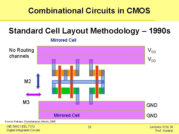
Combinational Circuits in CMOS Standard Cell Layout Methodology – 1990 s Mirrored Cell No Routing channels VDD M 2 M 3 GND Mirrored Cell GND Source: Rabaey; Chandrakasan; Nikolic, 2005 INE 5442 / EEL 7312 Digital Integrated Circuits 39 Lectures 33 to 36 Prof. Güntzel

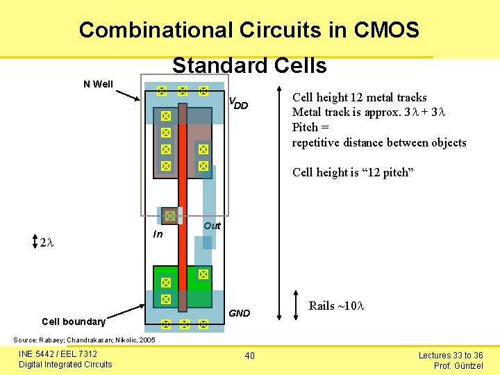
Combinational Circuits in CMOS Standard Cells N Well VDD Cell height 12 metal tracks Metal track is approx. 3 + 3 Pitch = repetitive distance between objects Cell height is “ 12 pitch” 2 In Cell boundary Out GND Rails ~10 Source: Rabaey; Chandrakasan; Nikolic, 2005 INE 5442 / EEL 7312 Digital Integrated Circuits 40 Lectures 33 to 36 Prof. Güntzel

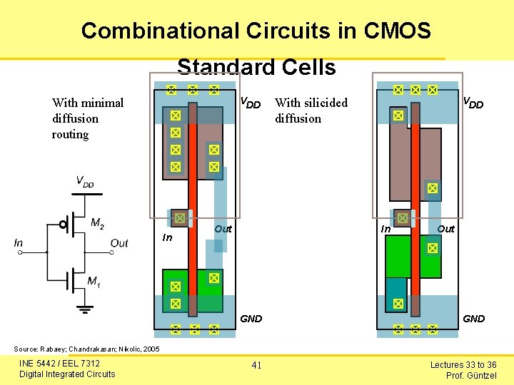
Combinational Circuits in CMOS Standard Cells VDD With minimal diffusion routing In Out VDD With silicided diffusion In GND Out GND Source: Rabaey; Chandrakasan; Nikolic, 2005 INE 5442 / EEL 7312 Digital Integrated Circuits 41 Lectures 33 to 36 Prof. Güntzel

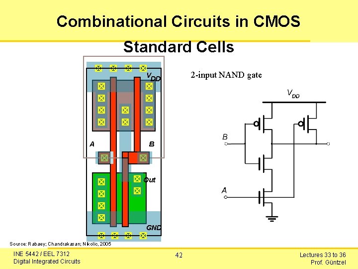
Combinational Circuits in CMOS Standard Cells 2 -input NAND gate VDD A B Out GND Source: Rabaey; Chandrakasan; Nikolic, 2005 INE 5442 / EEL 7312 Digital Integrated Circuits 42 Lectures 33 to 36 Prof. Güntzel

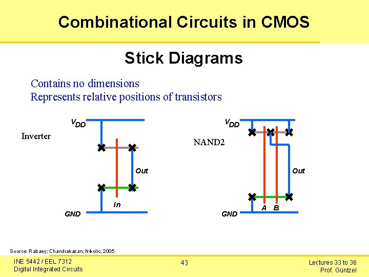
Combinational Circuits in CMOS Stick Diagrams Contains no dimensions Represents relative positions of transistors VDD Inverter NAND 2 Out In GND A B Source: Rabaey; Chandrakasan; Nikolic, 2005 INE 5442 / EEL 7312 Digital Integrated Circuits 43 Lectures 33 to 36 Prof. Güntzel

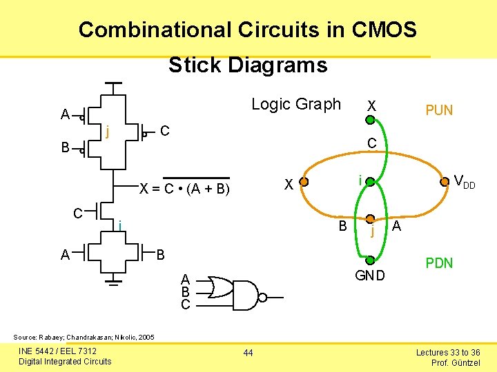
Combinational Circuits in CMOS Stick Diagrams Logic Graph A j X C C B i A i X X = C • (A + B) C PUN B VDD j B GND A B C A PDN Source: Rabaey; Chandrakasan; Nikolic, 2005 INE 5442 / EEL 7312 Digital Integrated Circuits 44 Lectures 33 to 36 Prof. Güntzel

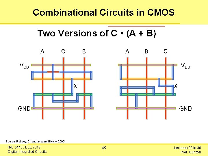
Combinational Circuits in CMOS Two Versions of C • (A + B) A C B A B C VDD X X GND Source: Rabaey; Chandrakasan; Nikolic, 2005 INE 5442 / EEL 7312 Digital Integrated Circuits 45 Lectures 33 to 36 Prof. Güntzel

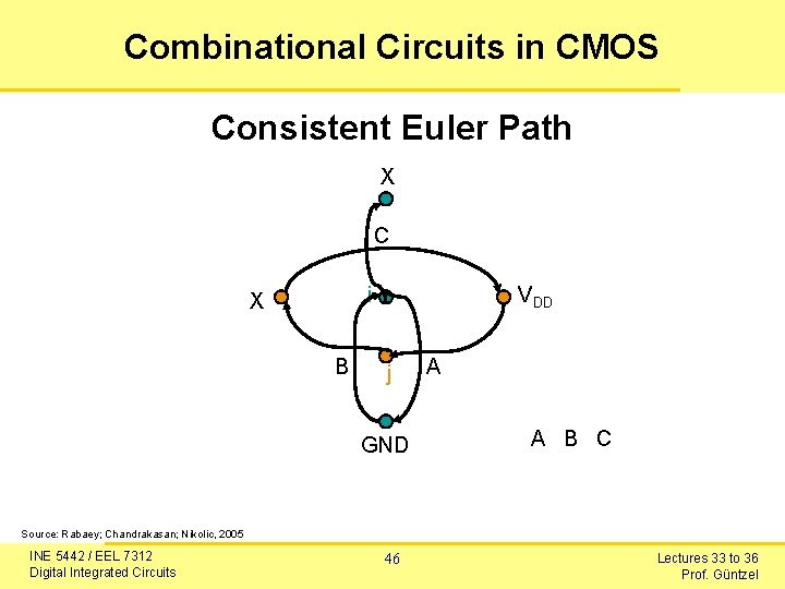
Combinational Circuits in CMOS Consistent Euler Path X C i X B VDD j GND A A B C Source: Rabaey; Chandrakasan; Nikolic, 2005 INE 5442 / EEL 7312 Digital Integrated Circuits 46 Lectures 33 to 36 Prof. Güntzel

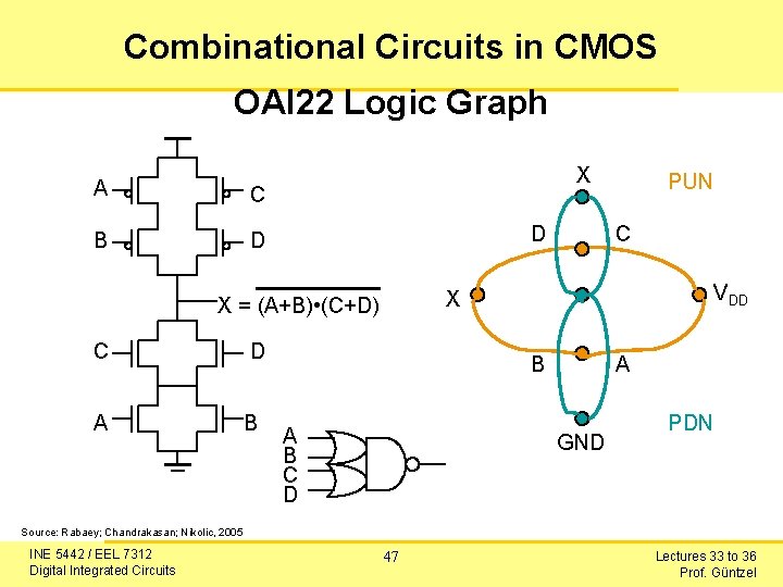
Combinational Circuits in CMOS OAI 22 Logic Graph A C B D X D D A B C VDD X X = (A+B) • (C+D) C PUN B A B C D A GND PDN Source: Rabaey; Chandrakasan; Nikolic, 2005 INE 5442 / EEL 7312 Digital Integrated Circuits 47 Lectures 33 to 36 Prof. Güntzel

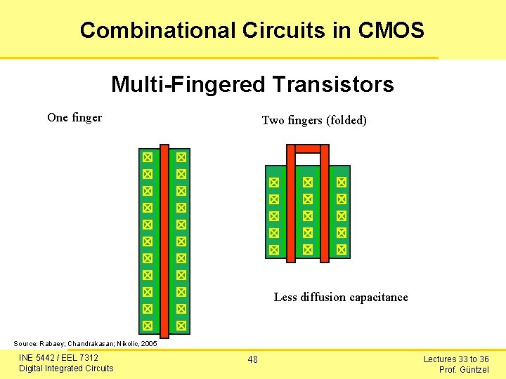
Combinational Circuits in CMOS Multi-Fingered Transistors One finger Two fingers (folded) Less diffusion capacitance Source: Rabaey; Chandrakasan; Nikolic, 2005 INE 5442 / EEL 7312 Digital Integrated Circuits 48 Lectures 33 to 36 Prof. Güntzel

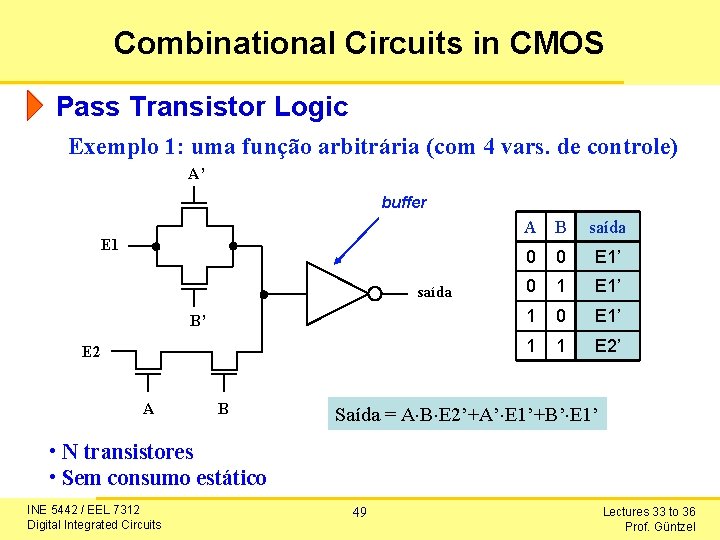
Combinational Circuits in CMOS Pass Transistor Logic Exemplo 1: uma função arbitrária (com 4 vars. de controle) A’ buffer A B E 1 saída B’ E 2 A B saída 0 0 E 1’ 0 1 E 1’ 1 0 E 1’ 1 1 E 2’ Saída = A B E 2’+A’ E 1’+B’ E 1’ • N transistores • Sem consumo estático INE 5442 / EEL 7312 Digital Integrated Circuits 49 Lectures 33 to 36 Prof. Güntzel
![Combinational Circuits in CMOS O Comportamento do Transistor de Passagem 3 0 Tensão V Combinational Circuits in CMOS O Comportamento do Transistor de Passagem 3. 0 Tensão [V]](https://slidetodoc.com/presentation_image/2f1d14100b54c4856e5e455d970a8ba2/image-50.jpg)
Combinational Circuits in CMOS O Comportamento do Transistor de Passagem 3. 0 Tensão [V] In Out 2. 0 x 1. 0 0 0. 5 1 1. 5 2 Tempo [ns] • ~ Vx não consegue atingir Vdd, mas Vdd -VTn(Vx) (efeito de corpo) • Tensão na entrada do inversor não é suficiente para desligar o transistor PMOS • Mensagem: não cascatear transistores de passagem, conectando-os a gates de outras estruturas similares. Source: Rabaey; Chandrakasan; Nikolic, 2005 INE 5442 / EEL 7312 Digital Integrated Circuits 50 Lectures 33 to 36 Prof. Güntzel

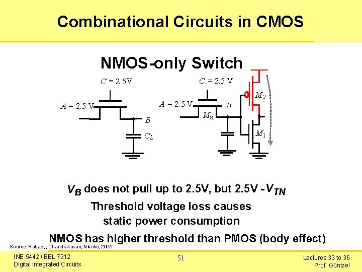
Combinational Circuits in CMOS NMOS-only Switch C = 2. 5 V C = 2. 5 V A = 2. 5 V B M 2 Mn B M 1 CL VB does not pull up to 2. 5 V, but 2. 5 V - VTN Threshold voltage loss causes static power consumption NMOS has higher threshold than PMOS (body effect) Source: Rabaey; Chandrakasan; Nikolic, 2005 INE 5442 / EEL 7312 Digital Integrated Circuits 51 Lectures 33 to 36 Prof. Güntzel

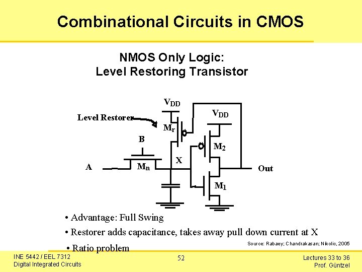
Combinational Circuits in CMOS NMOS Only Logic: Level Restoring Transistor VDD Level Restorer VDD Mr B A Mn M 2 X Out M 1 • Advantage: Full Swing • Restorer adds capacitance, takes away pull down current at X Source: Rabaey; Chandrakasan; Nikolic, 2005 • Ratio problem INE 5442 / EEL 7312 Digital Integrated Circuits 52 Lectures 33 to 36 Prof. Güntzel
![Combinational Circuits in CMOS Restorer Sizing Voltage V 3 0 2 0 Upper Combinational Circuits in CMOS Restorer Sizing Voltage [V] 3. 0 2. 0 • Upper](https://slidetodoc.com/presentation_image/2f1d14100b54c4856e5e455d970a8ba2/image-53.jpg)
Combinational Circuits in CMOS Restorer Sizing Voltage [V] 3. 0 2. 0 • Upper limit on restorer size • Pass-transistor pull-down can have several transistors in stack W/Lr =1. 75/0. 25 W/L r =1. 50/0. 25 1. 0 W/Lr =1. 0/0. 25 0. 0 0 100 200 W/L r =1. 25/0. 25 300 Time [ps] 400 500 Source: Rabaey; Chandrakasan; Nikolic, 2005 INE 5442 / EEL 7312 Digital Integrated Circuits 53 Lectures 33 to 36 Prof. Güntzel

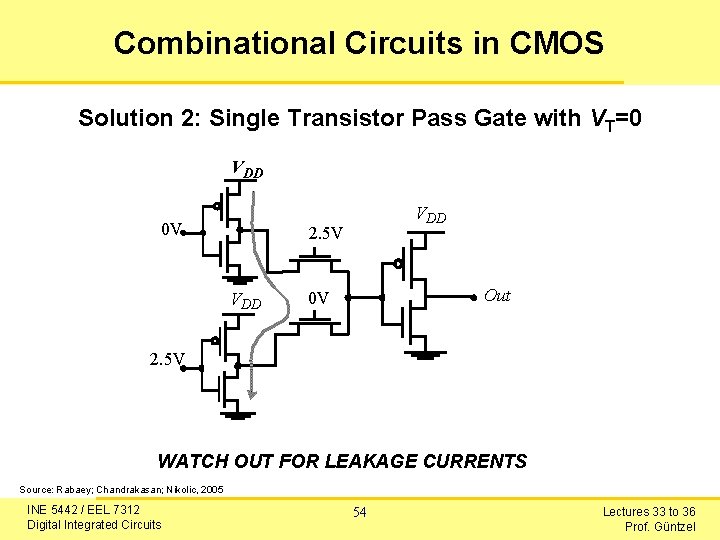
Combinational Circuits in CMOS Solution 2: Single Transistor Pass Gate with VT=0 VDD 0 V VDD 2. 5 V VDD Out 0 V 2. 5 V WATCH OUT FOR LEAKAGE CURRENTS Source: Rabaey; Chandrakasan; Nikolic, 2005 INE 5442 / EEL 7312 Digital Integrated Circuits 54 Lectures 33 to 36 Prof. Güntzel

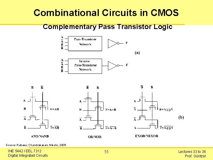
Combinational Circuits in CMOS Complementary Pass Transistor Logic Source: Rabaey; Chandrakasan; Nikolic, 2005 INE 5442 / EEL 7312 Digital Integrated Circuits 55 Lectures 33 to 36 Prof. Güntzel

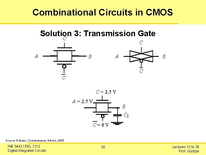
Combinational Circuits in CMOS Solution 3: Transmission Gate C A B B C C C = 2. 5 V A = 2. 5 V B CL C=0 V Source: Rabaey; Chandrakasan; Nikolic, 2005 INE 5442 / EEL 7312 Digital Integrated Circuits 56 Lectures 33 to 36 Prof. Güntzel

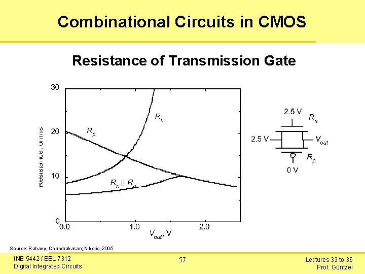
Combinational Circuits in CMOS Resistance of Transmission Gate Source: Rabaey; Chandrakasan; Nikolic, 2005 INE 5442 / EEL 7312 Digital Integrated Circuits 57 Lectures 33 to 36 Prof. Güntzel

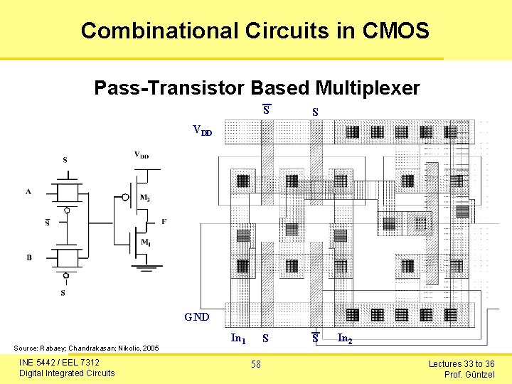
Combinational Circuits in CMOS Pass-Transistor Based Multiplexer S S VDD GND Source: Rabaey; Chandrakasan; Nikolic, 2005 INE 5442 / EEL 7312 Digital Integrated Circuits In 1 58 In 2 Lectures 33 to 36 Prof. Güntzel

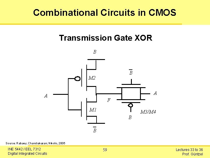
Combinational Circuits in CMOS Transmission Gate XOR B B M 2 A A F M 1 B M 3/M 4 B Source: Rabaey; Chandrakasan; Nikolic, 2005 INE 5442 / EEL 7312 Digital Integrated Circuits 59 Lectures 33 to 36 Prof. Güntzel

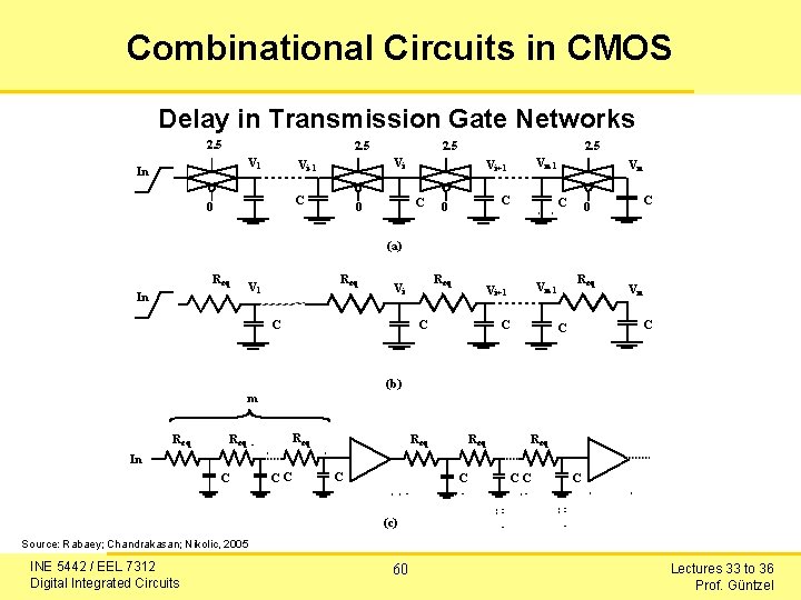
Combinational Circuits in CMOS Delay in Transmission Gate Networks 2. 5 V 1 In 2. 5 Vi Vi-1 C 0 2. 5 C 0 Vn-1 Vi+1 C 0 Vn C C 0 (a) Req In Req V 1 Req Vi C Vn-1 Vi+1 C C Req Vn C C (b) m Req Req Req In C CC C (c) Source: Rabaey; Chandrakasan; Nikolic, 2005 INE 5442 / EEL 7312 Digital Integrated Circuits 60 Lectures 33 to 36 Prof. Güntzel

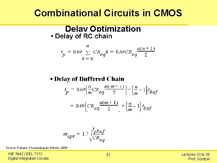
Combinational Circuits in CMOS Delay Optimization Source: Rabaey; Chandrakasan; Nikolic, 2005 INE 5442 / EEL 7312 Digital Integrated Circuits 61 Lectures 33 to 36 Prof. Güntzel

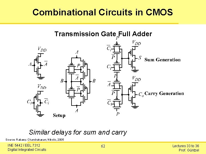
Combinational Circuits in CMOS Transmission Gate Full Adder Similar delays for sum and carry Source: Rabaey; Chandrakasan; Nikolic, 2005 INE 5442 / EEL 7312 Digital Integrated Circuits 62 Lectures 33 to 36 Prof. Güntzel