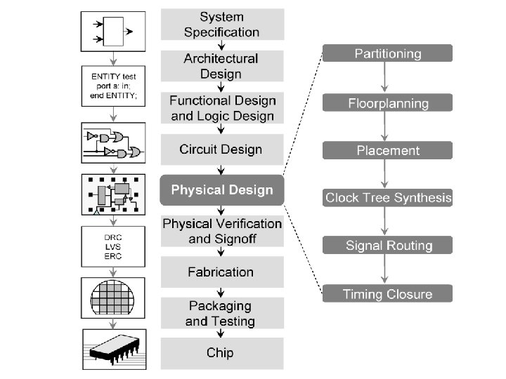
UNITV VHDL Synthesis VHDL Synthesis Circuit Design Flow


 to verify the functional")

 to")

 Physical")

.")


 is a specialized computer")


 to verify the")


is defined as the physical defect of one (or) more components (or)")
 General approach a) Permanent faults b)Temporary faults i) Transient faults ii) Intermediate faults")

 Logical approach a) Logical faults i) Stuck at faults a) Stuck at ‘")


: ØThe test generation & its application become expansive as")


.")
 test Single Input Change (SIC) test")
")


")


- Slides: 94
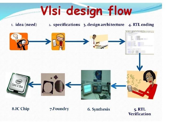
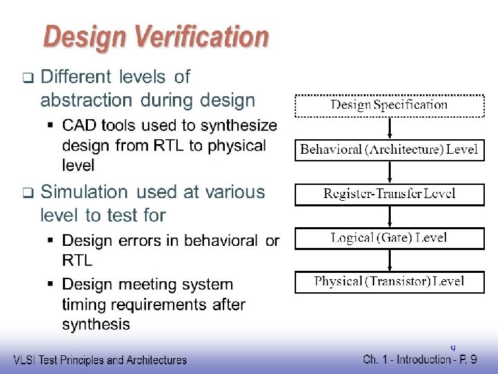
UNIT-V VHDL Synthesis: VHDL Synthesis, Circuit Design Flow, Circuit Synthesis, Simulation, Layout, Design capture tools, Design Verification Tools. Test and Testability: Fault-modelling and simulation, test generation, design for testability, Built-inself-test.
Circuit Design Flow:
Simulation is the process of using a simulation software (simulator) to verify the functional correctness of a digital design that is modeled using a HDL (hardware description language) like VHDL and Verilog. Types of Simulations: . • Behavioral simulation • Functional simulation • Gate-level simulation • Switch-level simulation • Transistor-level or circuit-level simulation
Synthesis is a process in which a design behavior that is modeled using a HDL is translated into an implementation consisting of logic gates. This is done by a synthesis tool which is another software program
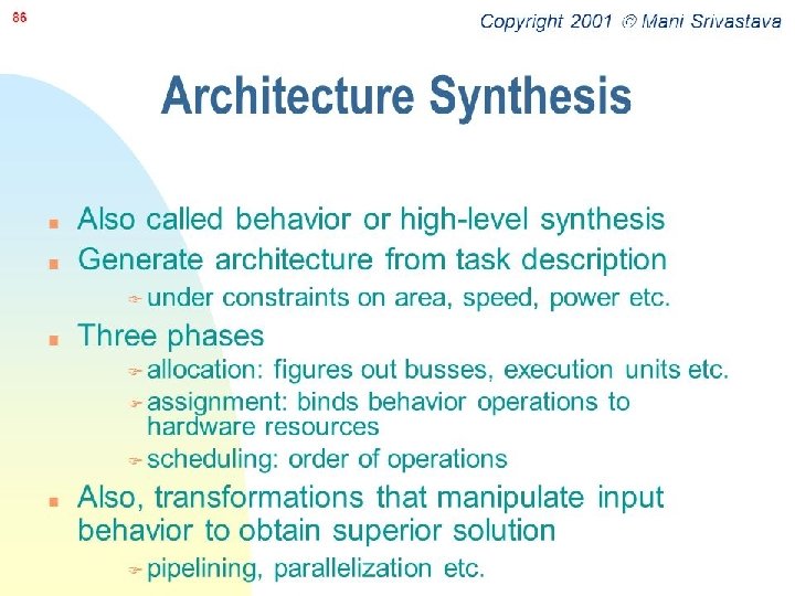
Synthesis – The Process of converting one representation of a circuit (source representation) to another functionally equivalent representation (target representation). Types: 1. Circuit Synthesis 2. Logic Synthesis 3. Architecture Synthesis
Structural Behavioral Synthesis ic ys Ph al n sig De Physical
Structural Behavioral Processor Memory Bus Algorithm Flowchart PCBs MCMs(Multichip module) Physical
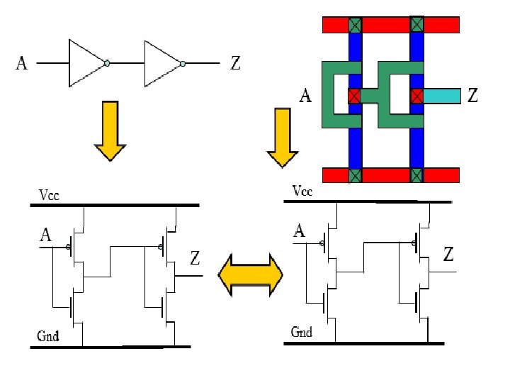
Circuit Synthesis § Synthesis is the process to convert a circuit description written in HDL to gate level description. module my_module input i 1 , …. ; output out 1 , …. ; reg …. wire … always @(…. . ) nand 2 n 1 (…) Dff d 1 (. . )
Logic Synthesis • Convert from logic equations to gate-level netlists (assume combinational logic). – Maximize speed – Minimize area, power a’bc + abc + d b b c c d d
Taxonomy of Synthesis Tasks
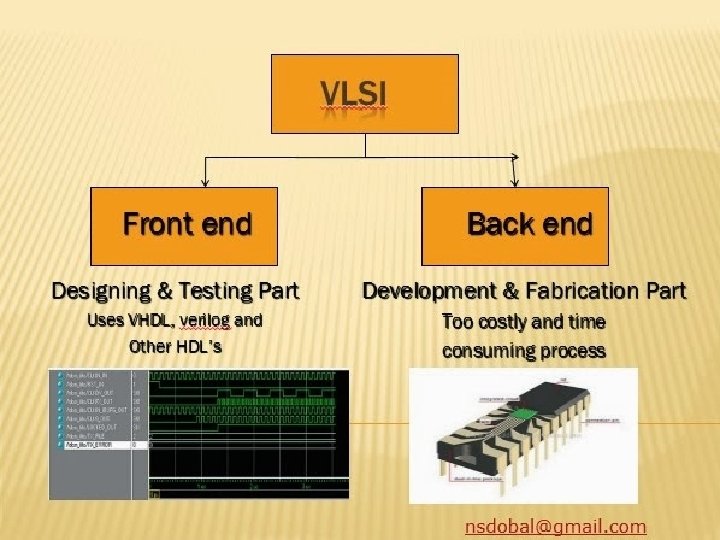
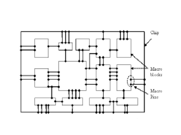
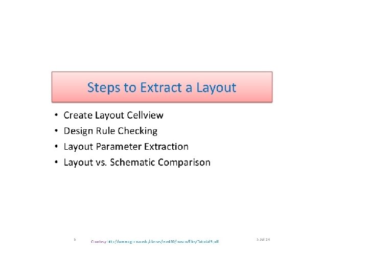
Design Capture Tools: 1. 2. 3. 4. 5. HDL Design Schematic Design Layout Design Floor Planning Chip Composition
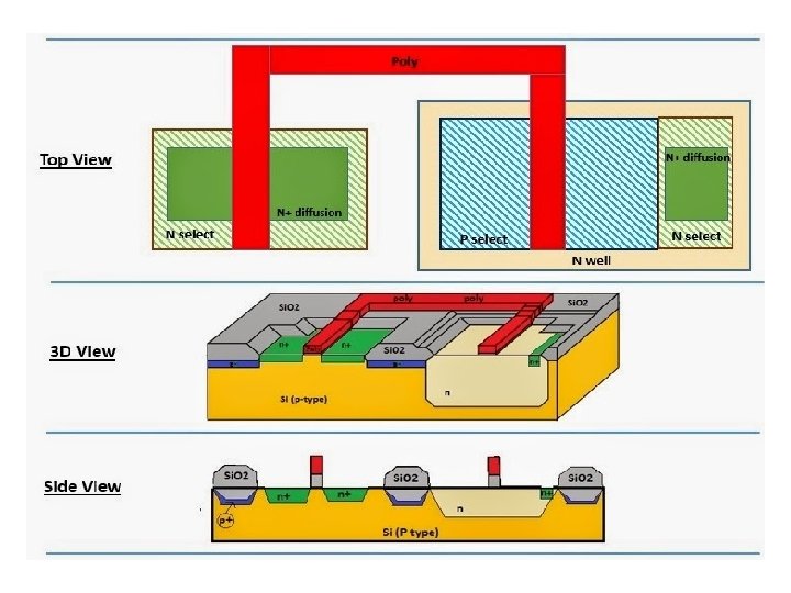
HDL Design: In computer engineering, a hardware description language (HDL) is a specialized computer language used to describe the structure and behavior of electronic circuits, and most commonly, digital logic circuits
Schematic Design:
Layout Design:
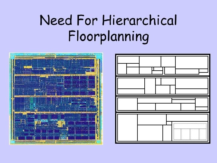
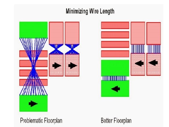
Floor planning must take into account blocks of varying function , size, shape. Must design: • space allocation • signal routing • power supply routing • clock distribution
Chip Composition:
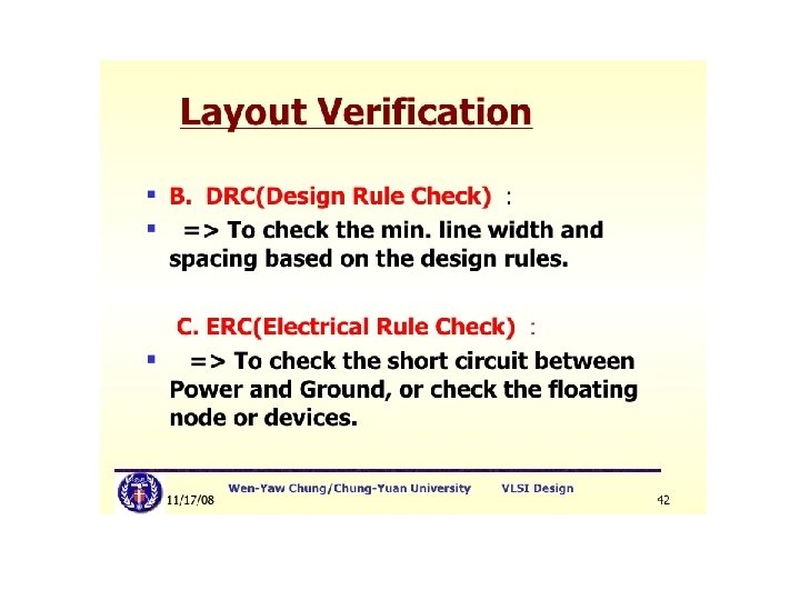
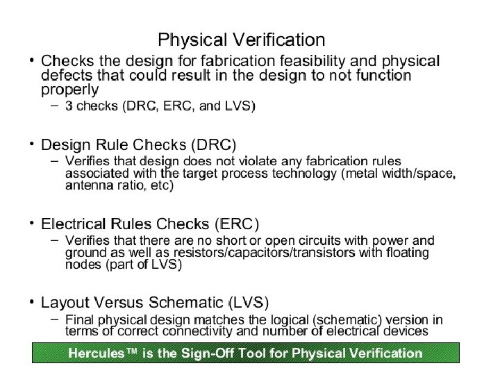
Design Verification Tools:
1. 2. 3. 4. 5. 6. 7. 8. Simulation Timing Verifiers Network Isomorphism Netlist Comparison Layout Extraction Back Annotation Design rule Verification Pattern generation
Simulation: Simulation is the process of using a simulation software (simulator) to verify the functional correctness of a digital design that is modeled using a HDL (hardware description language) like Verilog 1. 2. 3. 4. Circuit level Timing simulator Logic level Switch level
Timing Verifiers: Timing simulation is called post-route simulation because it confirms that your design is compatible with the timing and propagation delays that exist in a specific device.
Network Isomorphism: Network Isomorphism An electrical network may be represented by a graph where the vertices of the graph are devices such as MOS transistors, bipolar transistors, diodes, resistors, and capacitors. The arcs are the connections between devices. These are the electrical nodes in the circuit. Network Isomorphism is used to prove that two networks are equivalent and therefore and should function equivalently. This is used most often to prove that layout is equivalent to network extracted from schematic or HDL structural netlist.
Netlist Comparison The process of comparing two networks is commonly called netlist comparison.
Back annotation Often want to iteratively improve design. Back annotation updates a more-abstract design with information from later design stages. • Example: annotate logic schematic with extracted parasitic Rs and Cs.
Layout Extraction:
Design rule Verification:
Pattern generation:
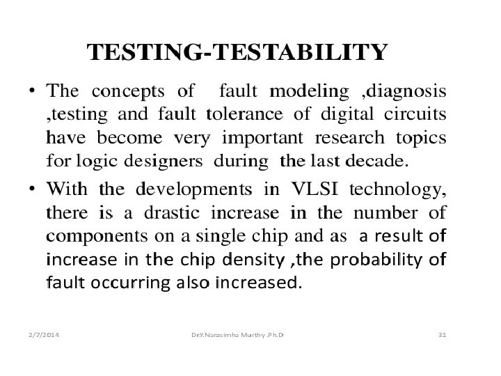
Test and Testability
Fault-modelling: Fault (Malfunction)is defined as the physical defect of one (or) more components (or) the connections between the components in the given circuit. Faults can be occur in many ways 1) General approach 2) Logical approach
1) General approach a) Permanent faults b)Temporary faults i) Transient faults ii) Intermediate faults
Permanent faults: Ø It is also called hard fault. Ø A fault that is occurred due to breaking of a component Ø or wire is called as permanent fault. Ø This fault is stay with device upto replacementof breaking component. Temporary faults: This kind of fault may occur at certain time intervals. i) Transient faults: The fault which is occurred due to some power supply fluctuations. ii) Intermediate faults: This kind of fault is occurred due to the component misbehaviour sometimes this turns into permanent faults.
2) Logical approach a) Logical faults i) Stuck at faults a) Stuck at ‘ 0’ fault b) Stuck at ‘ 1’ fault ii) Bridging faults a) AND type b) OR type iii) Cross point faults b) Parametric faults
Logical faults: This kind of fault change the boolean function obtained by the given circuit A B Y Actually Y=AB. but Y=A+B
Stuck at fault : A circuit node is permanently fixed to a logical value. a) Stuck at ‘ 0’ fault b) Stuck at ‘ 1’ fault When the signal line always present at logical ‘ 0’ is referred as Stuck-at-0 fault. When the signal line always present at logical ‘ 1’ is referred as Stuck-at-1 fault.
Bridging fault: This kind of faults are occurred if the signal lines are short at together. It may be either a) AND type bridge fault or b) OR type bridge fault.
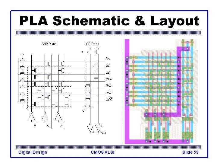
Cross point faults: These faults are occurred in PLA or PAL’s due to missing extra cross point. Parametric faults: Ø It is also called soft fault. Parametric faults are those changes that cause performance degradation of the circuit. Ø ØThese faults are due to the process fluctuations. These faults involve parameters' deviations from their nominal value that can consequently quit their tolerance band.
Test Vector Generation Fault Models A Fault Model is a description, at the digital logic level, of the effects of some fault or combination of faults in the underlying circuitry. The use of fault models has some advantages and also some disadvantages. · Advantages o Technology independent. o Works quite well in practice. · Disadvantages o May fail to identify certain process specific faults, for instance CMOS floating gates. o Detects static faults only.
Test vector: The input combination in which the presence of fault produces an output that is different from fault free output is known as Test vector.
Fault Models • Stuck-at-0 fault • Stuck-at-1 fault • Bridge fault • Stuck-open fault • Stuck-closed (stuck-on) fault • Path sensitization • Fault simulation
Stuck-at-0 fault Stuck-at-1 fault
Bridging fault:
Some other Fault Models : Stuck-open fault: At the switch level, a transistor can be stuck-off or stuck-on, also referred to as stuck-open or stuck short, respectively A stuck open transistor fault in a CMOS combinational logic gate can cause the gate to behave like a levelsensitive latch
Stuck-Closed fault: Stuck-short faults, on the other hand, can produce a conducting path between power (VDD) and ground (VSS) and may be detected by monitoring the power supply current during steady state
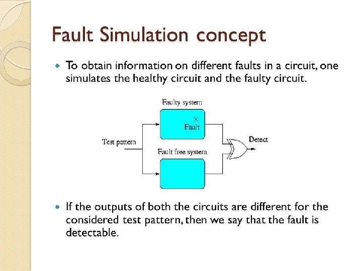
Test vector generation Fault simulation Boolean differences Path sensitization
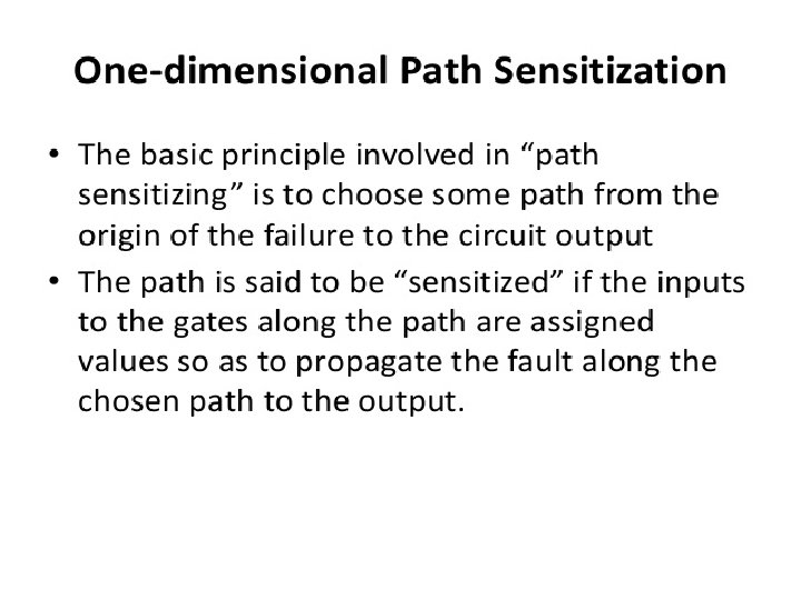
Path sensitization Fault sensitization: In this step a stuck-at fault is activated by setting the signal driving the faulty net to an opposite value from the fault value.
Design for Testability: The keys to designing circuits that are testable are • Controllability • Observability. Controllability : The ability to set (1) or reset (0) every node internal to the circuit. Observability: The ability to Observe either directly or indirectly the state of any node in the circuit. Good controllability and observability reduce cost of manufacturing test they allow high fault coverage with relatively few test vectors.
They are mainly two approaches for Design for Testability. 1. Ad. hoc testing 2. Structued testing a. scan b. partial scan c. Built in self test. d. Boundaryc scan test.
1. Ad. hoc testing: It is mainly used to test random logic i. e for multilevel standard cell , two level PLA. It is a collection of ideas aimed at reducing the combinational explosion of testing. Ø This approaches are used when ATPG and BIST are unavailable. Ø These are mainly used for small designs when ATPG & are BIST unavailable.
Common Techniques for Adhoc testing involve Ø Partitioning large sequential circuits Ø Adding test points Ø Adding multiplexer Ø Providing for easy state reset.
2. Scan-Based approach: The main difficulty in testing of sequential circuits is in determining internal state of the circuit. In scan design technique the controllability & observability of the internal states is improved.
Scan-Path Technique
The testing of sequential logic may be made easier in following ways 1. Serial scan 2. Parallel Scan 3. LSSD(Level- sensitive scan design) 4. Boundary Scan.
3. Built in self test(BIST): ØThe test generation & its application become expansive as the complexity of individual VLSI circuit & Overall system is increased. ØThe complexity & controlling even become more problem when we are designing VLSI for very high speed operation.
The BIST has been proposed with objective of 1. To reduce the test pattern generation cost 2. To decrease the volume of test data. 3. To decrease the time required for testing. Some test scheme under BIST are Ø Signature Analysis Ø Built in logic block observer Ø Self checking test
Controllability Observability 1. Controllability - Being able to set up known internal states. 2. Observability - Being able to observe the effects of a state change as it occurs (preferably at the system primary outputs).
pseudo-random binary sequence (PRBS).
Multiple Input Change (MIC) test Single Input Change (SIC) test
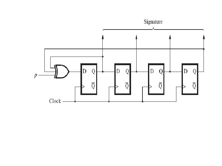
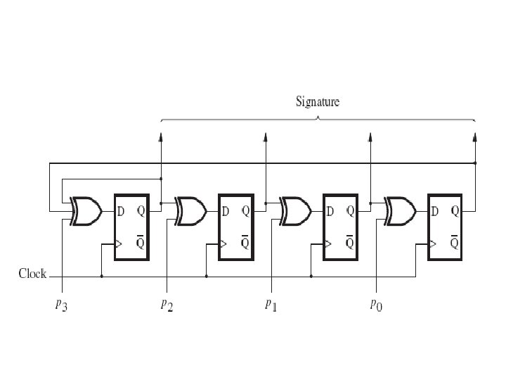
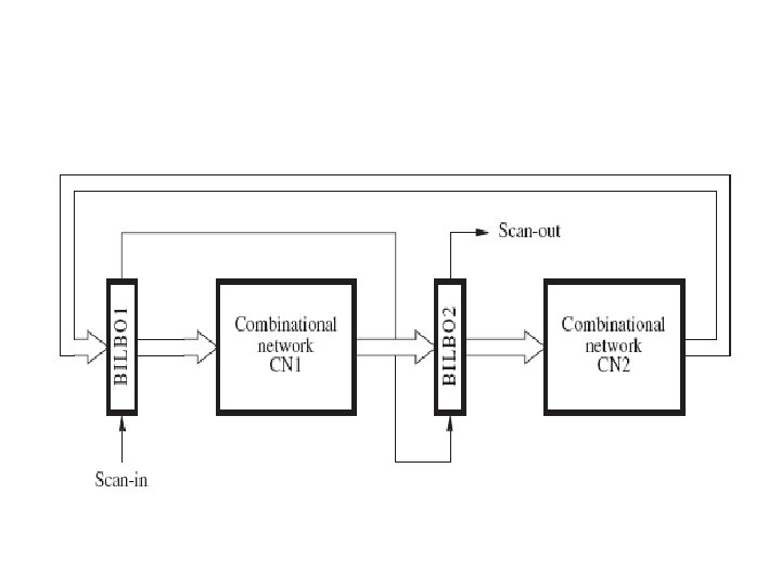
Built-in Logic Block Observer (BILBO)
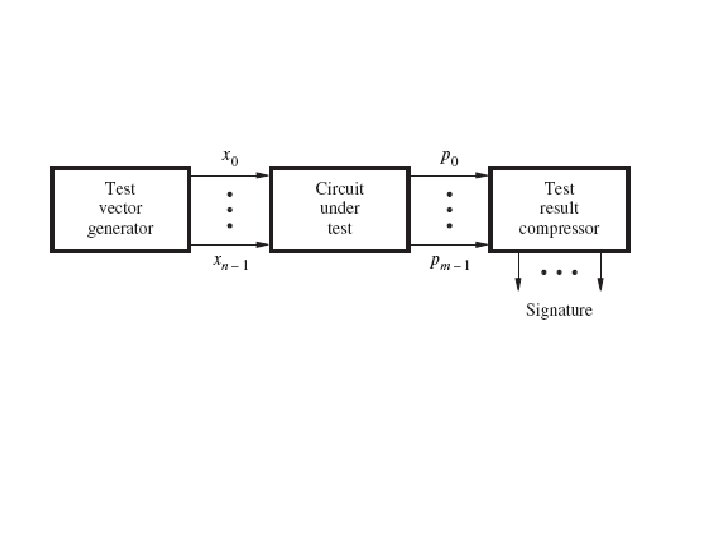
The essence of BIST is to have internal capability for generation of tests and for compression of the results. Instead of using separate circuits for these two functions, it is possible to design a single circuit that serves both purposes. Figure shows the structure of a possible circuit, known as the built-in logic block observer (BILBO).
First, BILBO 1 is used as a PRBS generator that provides test patterns for combinational network 1 (CN 1). During this time BILBO 2 acts as a compressor and produces a signature for the test The signature is shifted out by placing BILBO 2 into the shift-register mode. Next, the roles of BILBO 1 and BILBO 2 are reversed, and the process is repeated to test CN 2.
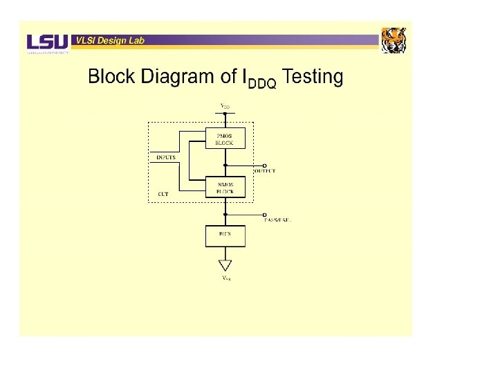
Iddq testing: Iddq testing is a method for testing CMOS integrated circuits for the presence of manufacturing faults. It relies on measuring the supply current (Idd) in the quiescent state (when the circuit is not switching and inputs are held at static values)
Iddq testing has many advantages: §It is a simple and direct test that can identify physical defects. §The area and design time overhead are very low. §Test generation is fast. §Test application time is fast since the vector sets are small. Drawback: § Compared to scan chain testing, Iddq testing is time consuming, and thus more expensive, as is achieved by current measurements that take much more time than reading digital pins in mass production.
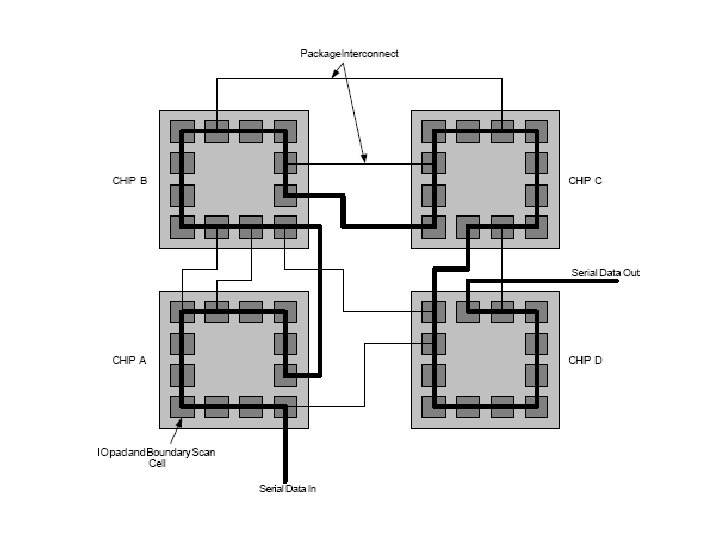
Boundary scan test (BST)
• Test the interconnections between the various chips on the board; • Deliver test data to the chips on the board for selftesting; • Test the chips themselves with internal self-test facilities. The advantages of BST are seen as follows: • no need for complex testers in PCB testing; • the test engineer's work is simplified and efficient; • the time spent on test pattern generation and application is reduced; • fault coverage is increased.
Boundary scan is accessed through five pins – TCK: test clock – TMS: test mode select – TDI: test data in – TDO: test data out – TRST*: test reset (optional)
Built-in Logic Block Observer Signature Analysis Boundary Scan