UnitII Introduction to Microcontroller 8051 15 Lectures Features
 • Features, Pin diagram, functional")


: X 2 and")


 • As we know that the")


 Bank Select Bits, RS 1, & RS 0 to select")

 The 8051 Microcontroller Special Function Registers act as")
 along with their functions and")
 The Accumulator or Register A is")
 The B Register is used along with the ACC in Multiplication")
 The PSW or Program Status Word Register is also called")

 The Data Pointer is a")
 SP or Stack Pointer points out to the top of the")
 The 8051")
 The PCON or Power Control register, as the")
 The Serial Control or SCON SFR is used to control the")
 The TMOD or Timer Mode register or SFR is used to")
 The IE or Interrupt Enable Register is used to enable or")
 The Serial Buffer or SBUF register is")
 The TL 1 and TH 1 are the")


- Slides: 40
• Unit-II: Introduction to Microcontroller 8051 (15 Lectures) • Features, Pin diagram, functional pin diagram and pin description, Architecture, Reset, Memory organization, CPU timings.
Features of 8051 Microcontroller : • • • • • An 8051 microcontroller comes bundled with the following features − 4 KB bytes on-chip program memory (ROM) 128 bytes on-chip data memory (RAM) Four register banks 128 user defined software flags 8 -bit bidirectional data bus 16 -bit unidirectional address bus 32 general purpose registers each of 8 -bit 16 bit Timers (usually 2, but may have more or less) Three internal and two external Interrupts Four 8 -bit ports, (short model have two 8 -bit ports) 16 -bit program counter and data pointer It has 11 special function register. 1 Microsecond instruction cycle with 12 MHz Crystal. Multi mode high speed programmable full duplex serial port On chip Boolean processor It has 111 instructions, 64 instructions are single cycle. 8051 may also have a number of special features such as UARTs, ADC, Op -amp, etc.
Pin diagram, functional pin diagram and pin description
• functional pin diagram and pin description • • • The pin diagram of 8051 microcontroller consists of 40 pins as shown below. A total of 32 pins are set away into four Ports such as P 0, P 1, P 2 and P 3. Where, each port contains 8 pins. Therefore, the microcontroller 8051’s pin diagram and explanation is given below. Port 1 (Pin 1 to Pin 8): Port 1 includes pin 1. 0 to pin 1. 7 and these pins can be configured as input or output pins. Pin 9 (RST): Reset pin is used to Reset 8051 Microcontroller by giving a positive pulse to this Pin. Port 3 (Pin 10 to 17): The Port 3 Pins are similar to port 1 pins and can be used as universal Input or output pins. These pins dual-function Pins and the function of each Pin is given as: Pin 10 (RXD): RXD pin is a Serial Asynchronous Communication Input or Serial synchronous Communication Output. Pin 11 (TXD): Serial Asynchronous Communication Output or Serial Synchronous Communication clock Output. Pin 12 (INT 0): Input of Interrupt 0 Pin 13 (INT 1): Input of Interrupt 1 Pin 14 (T 0): Input of Counter 0 clock Pin 15 (T 1): Input of Counter 1 clock Pin 16 (WR): Writing Signal to write content on external RAM. Pin 17 (RD): Reading Signal to read contents of external RAM.
• • Pin 18 and 19 (XTAL 2, XTAL 1): X 2 and X 1 pins are input output pins for the oscillator. These pins are used to connect an internal oscillator to the microcontroller. Pin 20 (GND): Pin 20 is a ground pin. Port 2 (Pin 21 to Pin 28): Port 2 includes pin 21 to pin 28 which can be configured as Input Output Pins. But, this is only possible when we don’t use any external memory. If we use external memory, then these pins will work as high order address bus (A 8 to A 15). Pin 29 (PSEN): This pin is used to enable external program memory. If we use an external ROM for storing the program, then logic 0 appears on it, which indicates Micro controller to read data from the memory. Pin 30 (ALE): Address Latch Enable pin is an active high-output signal. If we use multiple memory chips, then this pin is used to distinguish between them. This Pin also gives program pulse input during programming of EPROM. Pin 31 (EA): If we have to use multiple memories then the application of logic 1 to this pin instructs the Microcontroller to read data from both memories: first internal and then external. Port 0 (Pin 32 to 39): Similar to the port 2 and 3 pins, these pins can be used as input output pins when we don’t use any external memory. When ALE or Pin 30 is at 1, then this port is used as data bus: when the ALE pin is at 0, then this port is used as a lower order address bus (A 0 to A 7) Pin 40 (VCC): This VCC pin is used for power supply.
• In Short : • • • Pins 1 to 8 − These pins are known as Port 1. This port doesn’t serve any other functions. It is internally pulled up, bi-directional I/O port. Pin 9 − It is a RESET pin, which is used to reset the microcontroller to its initial values. Pins 10 to 17 − These pins are known as Port 3. This port serves some functions like interrupts, timer input, control signals, serial communication signals Rx. D and Tx. D, etc. Pins 18 & 19 − These pins are used for interfacing an external crystal to get the system clock. Pin 20 − This pin provides the power supply to the circuit. Pins 21 to 28 − These pins are known as Port 2. It serves as I/O port. Higher order address bus signals are also multiplexed using this port. Pin 29 − This is PSEN pin which stands for Program Store Enable. It is used to read a signal from the external program memory. Pin 30 − This is EA pin which stands for External Access input. It is used to enable/disable the external memory interfacing. Pin 31 − This is ALE pin which stands for Address Latch Enable. It is used to demultiplex the address-data signal of port. Pins 32 to 39 − These pins are known as Port 0. It serves as I/O port. Lower order address and data bus signals are multiplexed using this port. Pin 40 − This pin is used to provide power supply to the circuit.
Architecture of 8051 Microcontroller :
Architecture of 8051 • Central Processor Unit (CPU) • As we know that the CPU is the brain of any processing device of the microcontroller. It monitors and controls all operations that are performed on the Microcontroller units. The User has no control over the work of the CPU directly. It reads program written in ROM memory and executes them and do the expected task of that application. • Interrupts • As its name suggests, Interrupt is a subroutine call that interrupts of the microcontrollers main operations or work and causes it to execute any other program, which is more important at the time of operation. The feature of Interrupt is very useful as it helps in case of emergency operations. An Interrupts gives us a mechanism to put on hold the ongoing operations, execute a subroutine and then again resumes to another type of operations.
Continued • • The Microcontroller 8051 can be configured in such a way that it temporarily terminates or pause the main program at the occurrence of interrupts. When a subroutine is completed, Then the execution of main program starts. Generally five interrupt sources are there in 8051 Microcontroller. There are 5 vectored interrupts are shown in below INTO TFO INT 1 TF 1 R 1/T 1 Out of these, (INT 0) and (INT 1) are external interrupts that could be negative edge triggered or low level triggered. When All these interrupts are activated, set the corresponding flogs except for serial interrupt, . The interrupt flags are cleared when the processor branches to the interrupt service routine (ISR). The external interrupt flags are cleared when the processor branches to the interrupt service routine, provides the interrupt is a negative edge triggered whereas the timers and serial port interrupts two of them are external interrupts, two of them are timer interrupts and one serial port interrupt terminal in general.
Continued INTERRUPTS: pin 12 to 15 · The 8051 has five interrupts. · In this two interrupts are external interrupt as INT 0 (Low), INT 1 (Low) and the remaining three are internal interrupts as timer-0, timer-1 and serial port. · All interrupts are maskable and vectored interrupts.
Continued • Memory • Microcontroller requires a program which is a collection of instructions. This program tells microcontroller to do specific tasks. These programs require a memory on which these can be saved and read by Microcontroller to perform specific operations of a particular task. The memory which is used to store the program of the microcontroller is known as code memory or Program memory of applications. It is known as ROM memory of microcontroller also requires a memory to store data or operands temporarily of the micro controller. The data memory of the 8051 is used to store data temporarily for operation is known RAM memory. 8051 microcontroller has 4 K of code memory or program memory, that has 4 KB ROM and also 128 bytes of data memory of RAM.
INTERNAL MEMORY A functioning computer must have memory for program code bytes, commonly in ROM, and RAM memory for variable data that can be altered as the program runs 8051 has internal RAM (128 bytes) and ROM (4 Kbytes) 8051 uses the same address but in different memories for code and data Internal circuitry access the correct memory based on the nature of the operation in progress We Can add memory externally if needed Internal ROM occupies the code address space from 0000 H to 0 FFFH (Size = 4 K byte) Program addresses higher than 0 FFFH will automatically fetch code bytes from external program memory Code bytes can also be fetched exclusively from an external memory by connecting the external access pin (EA) to ground.
Memory organisation :
Register A register is a small place in a CPU that can store small amounts of the data used for performing various operations such as addition and multiplication and loads the resulting data on main memory. Registers contain the address of the memory location where the data is to be stored. The size of the register is very important for modern controllers. For instance, for a 64 -bit register, a CPU tries to add two 32 -bit numbers and gives a 64 -bit result. Types of Registers • The 8051 microcontroller contains mainly two types of registers: • General purpose registers (Byte addressable registers) • Special function registers (Bit addressable registers) The 8051 microcontroller consists of 256 bytes of RAM memory, which is divided into two ways, such as 128 bytes for general purpose and 128 bytes for special function registers (SFR) memory. The memory which is used for general purpose is called as RAM memory, and the memory used for SFR contains all the peripheral related registers like Accumulator, ‘B’ register, Timers or Counters, and interrupt related registers. • •
Program Status Word (PSW) Bank Select Bits, RS 1, & RS 0 to select 1 of 4 register bank
Memory :
8051 Microcontroller Special Function Registers (SFRs) The 8051 Microcontroller Special Function Registers act as a control table that monitor and control the operation of the 8051 Microcontroller. If you observe in Internal RAM Structure, the Address Space from 80 H to FFH is allocated to SFRs. Out of these 128 Memory Locations (80 H to FFH), there are only 21 locations that are actually assigned to SFRs. Each SFR has one Byte Address and also a unique name which specifies its purpose. Since the SFRs are a part of the Internal RAM Structure, you can access SFRs as if you access the Internal RAM. The main difference is the address space: first 128 Bytes (00 H to 7 FH) is for regular Internal RAM and next 128 Bytes (80 H to FFH) is for SFRs. There are many ways to categorize these 21 Special Function Registers but I find the following way as an appropriate one. The 21 Special Function Registers of 8051 Microcontroller are categorized in to seven groups. They are: Math or CPU Registers: A and B Status Register: PSW (Program Status Word) Pointer Registers: DPTR (Data Pointer – DPL, DPH) and SP (Stack Pointer) I/O Port Latches: P 0 (Port 0), P 1 (Port 1), P 2 (Port 2) and P 3 (Port 3) Peripheral Control Registers: PCON, SCON, TMOD, IE and IP Peripheral Data Registers: TL 0, TH 0, TL 1, TH 1 and SBUF
All the 21 8051 Microcontroller Special Function Registers (SFRs) along with their functions and Internal RAM Address is given in the following table.
Registers of 8051 : A or Accumulator (ACC) The Accumulator or Register A is the most important and most used 8051 Microcontroller SFRs. The Register A is located at the address E 0 H in the SFR memory space. The Accumulator is used to hold the data for almost all the ALU Operations. Some of the operations where the Accumulator is used are: Arithmetic Operations like Addition, Subtraction, Multiplication etc. Logical Operations like AND, OR, NOT etc. Data Transfer Operations (between 8051 and External Memory) The name “Accumulator” came from the fact this register is used to accumulate (or store) the result of all Arithmetic and most of the Logical Operations.
B (Register B) The B Register is used along with the ACC in Multiplication and Division operations. These two operations are performed on data that are stored only in Registers A and B. During Multiplication Operation, one of the operand (multiplier or multiplicand) is stores in B Register and also the higher byte of the result. In case of Division Operation, the B Register holds the divisor and also the remainder of the result. It can also be used as a General Purpose Register for normal operations and is often used as an Auxiliary Register by Programmers to store temporary results. Register B is located at the address F 0 H of the SFR Address Space.
Program Status Word (PSW) The PSW or Program Status Word Register is also called as Flag Register and is one of the important SFRs. The PSW Register consists of Flag Bits, which help the programmer in checking the condition of the result and also make decisions. Flags are 1 -bit storage elements that store and indicate the nature of the result that is generated by execution of certain instructions. The following image shows the contents of the PSW Register.
The following table describes the function of each flag.
Pointer Registers Data Pointer (DPTR – DPL and DPH) The Data Pointer is a 16 -bit Register and is physically the combination of DPL (Data Pointer Low) and DPH (Data Pointer High) SFRs. The Data Pointer can be used as a single 16 -bit register (as DPTR) or two 8 -bit registers (as DPL and DPH). DPTR doesn’t have a physical Memory Address but the DPL (Lower Byte of DPTR) and DPH (Higher Byte of DPTR) have separate addresses in the SFR Memory Space. DPL = 82 H and DPH = 83 H. The DPTR Register is used by the programmer addressing external memory (Program – ROM or Data – RAM).
Stack Pointer (SP) SP or Stack Pointer points out to the top of the Stack and it indicates the next data to be accessed. Stack Pointer can be accesses using PUSH, POP, CALL and RET Instructions. The Stack Pointer is an 8 -bit register and upon reset, the Stack Pointer is initialized with 07 H. When writing a new data byte into the stack, the SP (Stack Pointer) is automatically incremented by 1 and the new data is written at an address SP+1. When reading data from stack, the data is retrieved from the Address in SP and after that the SP is decremented by 1 (SP-1).
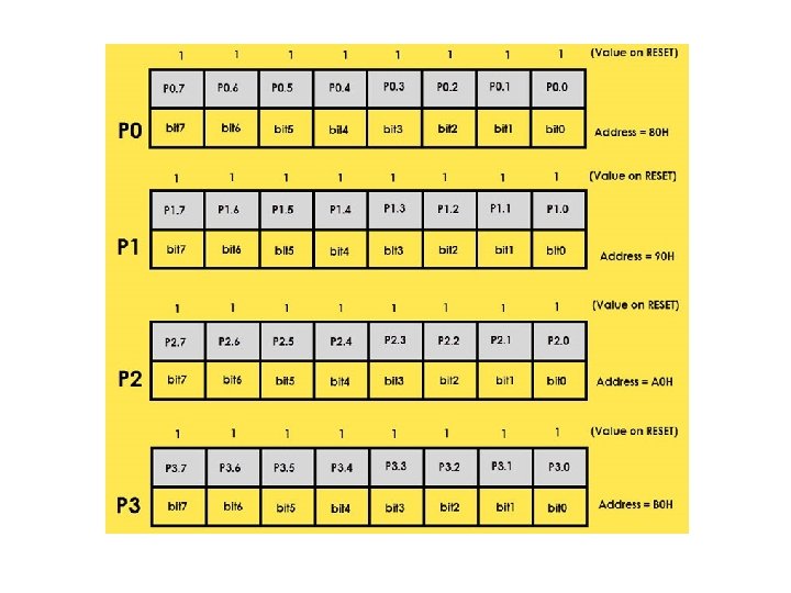
I/O Port Registers (P 0, P 1, P 2 and P 3) The 8051 Microcontroller four Ports which can be used as Input and/or Output. These four ports are P 0, P 1, P 2 and P 3. Each Port has a corresponding register with same names (the Port Registers are also P 0, P 1, P 2 and P 3). The addresses of the Port Registers are as follows: P 0 – 80 H, P 1 – 90 H, P 2 – A 0 H and P 2 – B 0 H. Each bit in these SFRs corresponds to one physical Pin in the 8051 Microcontroller. All these Port Registers are both Bit Addressable and Byte Addressable. Writing 1 or 0 on a Port Register Bit will reflect as an appropriate voltage (5 V and 0 V) on the corresponding Pin. If a Port Bit is SET (declared as 1), the corresponding Port Pin will be configured as Input and similarly if a Port Bit is CLEARED (declared as 0), the corresponding Port Pin is configured as Output. Upon reset, all the Port Bits are SET (1) and hence, all the Port Pins are configured as Inputs.
Peripheral Control Registers PCON (Power Control) The PCON or Power Control register, as the name suggests is used to control the 8051 Microcontroller’s Power Modes and is located at 87 H of the SFR Memory Space. Using two bits in the PCON Register, the microcontroller can be set to Idle Mode and Power Down Mode. During Idle Mode, the Microcontroller will stop the Clock Signal to the ALU (CPU) but it is given to other peripherals like Timer, Serial, Interrupts, etc. In order to terminate the Idle Mode, you have to use an Interrupt or Hardware Reset. In the Power Down Mode, the oscillator will be stopped and the power will be reduced to 2 V. To terminate the Power Down Mode, you have to use the Hardware Reset. Apart from these two, the PCON Register can also be used for few additional purposes. The SMOD Bit in the PCON Register is used to control the Baud Rate of the Serial Port. There are two general purpose Flag Bits in the PCON Register, which can be used by the programmer during execution.
SCON (Serial Control) The Serial Control or SCON SFR is used to control the 8051 Microcontroller’s Serial Port. It is located as an address of 98 H. Using SCON, you can control the Operation Modes of the Serial Port, Baud Rate of the Serial Port and Send or Receive Data using Serial Port. SCON Register also consists of bits that are automatically SET when a byte of data is transmited or received. TCON (Timer Control) Timer Control or TCON Register is used to start or stop the Timers of 8051 Microcontroller. It also contains bits to indicate if the Timers has overflowed. The TCON SFR also consists of Interrupt related bits.
TMOD (Timer Mode) The TMOD or Timer Mode register or SFR is used to set the Operating Modes of the Timers T 0 and T 1. The lower four bits are used to configure Timer 0 and the higher four bits are used to configure Timer 1. The Gatex bit is used to operate the Timerx with respect to the INTx pin or regardless of the INTx pin. GATE 1 ==> Timer 1 is operated only if INT 1 is SET. GATE 1 = 0 ==> Timer 1 is operates irrespective of INT 1 pin. GATE 0 = 1 ==> Timer 0 is operated only if INT 0 is SET. GATE 0 ==> Timer 0 is operates irrespective of INT 0 pin. The C/Tx bit is used selects the source of pulses for the Timer to count. C/T 1 ==> Timer 1 counts pulses from Pin T 1 (P 3. 5) (Counter Mode) C/T 1 = 0 ==> Timer 1 counts pulses from internal oscillator (Timer Mode) C/T 0 = 1 ==> Timer 0 counts pulses from Pin T 0 (P 3. 4) (Counter Mode) C/T 0 ==> Timer 0 counts pulses from internal oscillator (Timer Mode)
IE (Interrupt Enable) The IE or Interrupt Enable Register is used to enable or disable individual interrupts. If a bit is SET, the corresponding interrupt is enabled and if the bit is cleared, the interrupt is disabled. The Bit 7 of the IE register i. e. EA bit is used to enable or disable all the interrupts. IP (Interrupt Priority) The IP or Interrupt Priority Register is used to set the priority of the interrupt as High or Low. If a bit is CLEARED, the corresponding interrupt is assigned low priority and if the bit is SET, the interrupt is assigned high priority.
Peripheral Data Registers SBUF (Serial Data Buffer) The Serial Buffer or SBUF register is used to hold the serial data while transmission or reception. TL 0/TH 0 (Timer 0 Low/High) The Timer 0 consists of two SFRs: TL 0 and TH 0. The TL 0 is the lower byte and the TH 0 is the higher byte and together they form a 16 -bit Timer 0 Register.
TL 1/TH 1 (Timer 1 Low/High) The TL 1 and TH 1 are the lower and higher bytes of the Timer 0.
Continued • • • BUS Basically Bus is a collection of wires which work as a communication channel or medium for transfer of Data. These buses consists of 8, 16 or more wires of the microcontroller. Thus, these can carry 8 bits, 16 bits simultaneously. Hire two types of buses that are shown in below Address Bus Data Bus Address Bus: Microcontroller 8051 has a 16 bit address bus for transferring the data. It is used to address memory locations and to transfer the address from CPU to Memory of the microcontroller. It has four addressing modes that are Immediate addressing modes. Bank address (or) Register addressing mode. Direct Addressing mode. Register indirect addressing mode. Data Bus: Microcontroller 8051 has 8 bits of the data bus, which is used to carry data of particular applications.
Continued • Oscillator • Generally, we know that the microcontroller is a device, therefore it requires clock pulses for its operation of microcontroller applications. For this purpose, microcontroller 8051 has an on-chip oscillator which works as a clock source for Central Processing Unit of the microcontroller. The output pulses of oscillator are stable. Therefore, it enables synchronized work of all parts of the 8051 Microcontroller. • Input/Output Port • Normally microcontroller is used in embedded systems to control the operation of machines in the microcontroller. Therefore, to connect it to other machines, devices or peripherals we require I/O interfacing ports in the microcontroller interface. For this purpose microcontroller 8051 has 4 input, output ports to connect it to the other peripherals • Timers/Counters • 8051 microcontroller has two 16 bit timers and counters. These counters are again divided into a 8 bit register. The timers are used for measurement of intervals to determine the pulse width of pulses.
Signal Description
Continued • • • • The INTEL 805 F is an 8 -bit microcontroller with 128 byte internal RAM and 4 kb internal ROM. The INTEL 8031 is same, as 8051 except that it does not have internal ROM. The 8051 is a pin 40 pin IC available in Dual-In line package (DIP). Requires a single power supply of +5 V. Its maximum internal clock frequency rating is 12 MHz. Ports: (pin 1 to 8, pin 10 to 17, pin 21 to 28 and pin 32 to 39) · The 8031/8051 microcontroller has 32 I/O pins and they are organized as four numbers of 8 -bit parallel Ports : The ports are denoted as port-0, port-1, port-2 and port-3. Each port can be used as either 8 -bit parallel port or 8 numbers of 1 -bit ports. The ports behave as latches during output operation and behave as buffers during input operation. Port-1 can be used only for I/O operation · When external memory is employed, the port-0 function as multiplexed low byte address or data lines, and port-2 function as high byte address lines. Therefore for accessing external memory the microcontroller uses 16 -bit address and access the memory in bytes. Hence the addressable memory space is 64 kb (216 =64 kb). · The 8031/8051 allows the external memory to be organized as two banks of 64 kb. One is program/code memory and the other is data memory. PSEN (low signal): pin 29 The signal PSEN (low) is used as read control/enable for program memory. RD (low signal) and WR (low signal): pin 17 and pin 16 The port pin P 3. 7 function as read control and the port pin P 3. 6 function as write control for data memory.
Continued • • When external memory is employed, the port-0 function as multiplexed low byte address or data lines, and port-2 function as high byte address lines. Therefore for accessing external memory the microcontroller uses 16 -bit address and access the memory in bytes. Hence the addressable memory space is 64 kb (216 =64 kb). The 8031/8051 allows the external memory to be organized as two banks of 64 kb. One is program/code memory and the other is data memory. PSEN (low signal): pin 29 The signal PSEN (low) is used as read control/enable for program memory. RD (low signal) and WR (low signal): pin 17 and pin 16 · The port pin P 3. 7 function as read control and the port pin P 3. 6 function as write control for data memory. · When two external memory banks are not desirable, the PSEN (low) and RD (low) should be externally ANDed to provide a single read control signal. In such cases the controller will access a common memory space (of maximum capacity 64 kb) for program and data.
Continued • ALE is used to demultiplex the low byte address or data using an external latch. • EA (Low)/Vpp : pin 31 • When the microcontroller access program from external memory, then this pin is low. ie. EA (low) is enabled. • When the microcontroller access program from internal memory, then this pin is high. At that time this pin is used to supply programming voltage +12 V to EPROM/ROM. • XTAL 1 AND XTAL 2: PIN 19 AND PIN 18 • · The XTAL 1 and XTAL 2 pins are provided for external quartz crystal connection, in order to generate the required clock for the microcontroller. The maximum frequency of quartz crystal that can be connected to 8031/8051 microcontroller is 12 MHz. • RST (low): pin 9 • · The RST(low) signal is used to reset the microcontroller in order to bring the controller to a known state.
Applications of 8051 : • Some of the applications of 8051 is mainly used in daily life & industrial applications also some of that applications are shown below • Light sensing and controlling devices • Temperature sensing and controlling devices • Fire detections and safety devices • Automobile applications • Defense applications • Some industrial applications of micro controller and its applications • Industrial instrumentation devices • Process control devices • Some of 8051 microcontroller devices are used in measurement applications • Voltmeter applications • Measuring and revolving objects • Current meter objects • Hand held metering system • 8051 Microcontroller Applications in Embedded Systems
• • • • • The applications of 8051 microcontroller involves in 8051 based projects. Arduino Managed High Sensitive LDR based Power Saver for Street Light Control System The Temperature Humidity Monitoring System of Soil Based on Wireless Sensor Networks using Arduino RFID based Electronic Passport System for Easy Governance using Arduino based RFID Sensed Device Access Arduino based DC Motor Speed Control Arduino Based Line Following Robot Zigbee based Automatic Meter Reading System GSM based Electricity Energy Meter Billing with Onsite Display Android Phone Speech Recognition Sensed Voice Command based Notice Board Display Parking Availability Indication System Voice Controlled Home Appliances Remote Control Home Appliances PC Mouse operated Electrical Load Control Using VB Application Solar Highway Lighting System with Auto Turn Off in Daytime 8051 Microcontroller based Wireless Energy Meter Farmer Friendly Solar Based Electric Fence for Deterring Cattles Vehicle Movement Sensed Streetlight with Daytime auto off Features