UNITII BASIC COMPUTER ORGANIZATION AND DESIGN Bharati Vidyapeeths
UNIT-II BASIC COMPUTER ORGANIZATION AND DESIGN © Bharati Vidyapeeth’s Institute of Computer Applications and Management, New Delhi-63. , by Mrs. Manu Anand U 2. 1
LEARNING OBJECTIVES • System Bus • Instruction Codes • Computer Registers • Computer Instructions • Timing and Control • Instruction Cycle • Memory Reference Instructions • Input-Output and Interrupt • Complete Computer Description • Design of Basic Computer • Design of Accumulator Logic © Bharati Vidyapeeth’s Institute of Computer Applications and Management, New Delhi-63, by Mrs. Manu Anand U 2. 2
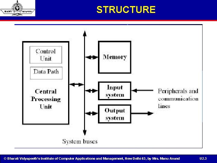
STRUCTURE © Bharati Vidyapeeth’s Institute of Computer Applications and Management, New Delhi-63, by Mrs. Manu Anand U 2. 3
SYSTEM BUSES • The major computer system components (processor, main memory, I/O modules) need to be interconnected in order to exchange data and control signals • A bus is a communication pathway connecting two or more devices • A bus that connects major computer components (processor, memory, I/O) is called a system bus. • Bus = a shared transmission medium. Only one device at a time Can successfully transmit. § shared system bus consisting of multiple lines § a hierarchy of buses to improve performance. • Key design elements for buses include: Arbitration, Timing, width © Bharati Vidyapeeth’s Institute of Computer Applications and Management, New Delhi-63, by Mrs. Manu Anand U 2. 4

SYSTEM BUSES © Bharati Vidyapeeth’s Institute of Computer Applications and Management, New Delhi-63, by Mrs. Manu Anand U 2. 5

MULTIPLE BUS HIERARCHIES • In general, the more devices attached to the bus, the greater the bus length and hence the greater the propagation delay. • The bus may become a bottleneck as the aggregate data transfer demand approaches the capacity of the bus. © Bharati Vidyapeeth’s Institute of Computer Applications and Management, New Delhi-63, by Mrs. Manu Anand U 2. 6
SYNCHRONOUS BUSES • Synchronous buses include a clock line between the control lines, line that is controlled by a clock quartz oscillator, usually between 5 - 133 MHz • All the transfers on the system bus has a fixed protocol related to the clock signal, and it is developed along an integer number of cycles, called bus cycles. • The advantages of a synchronous bus are a high speed of transfer, the very simple implied logic • The disadvantage comes from transfers that can be shorter than the time corresponding to the integer number of bus cycles. © Bharati Vidyapeeth’s Institute of Computer Applications and Management, New Delhi-63, by Mrs. Manu Anand U 2. 7
INTRODUCTION • Every different processor type has its own design (different registers, buses, microoperations, machine instructions, etc) • Modern processor is a very complex device • It contains § Many registers § Multiple arithmetic units, for both integer and floating point calculations § The ability to pipeline several consecutive instructions to speed execution etc. © Bharati Vidyapeeth’s Institute of Computer Applications and Management, New Delhi-63, by Mrs. Manu Anand U 2. 8
INTRODUCTION • However, to understand how processors work, we will start with a simplified processor model • This is similar to what real processors were like ~25 years ago • M. Morris Mano introduces a simple processor model he calls the Basic Computer • We will use this to introduce processor organization and the relationship of the RTL model to the higher level computer processor © Bharati Vidyapeeth’s Institute of Computer Applications and Management, New Delhi-63, by Mrs. Manu Anand U 2. 9
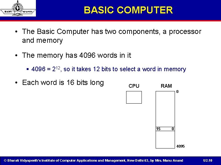
BASIC COMPUTER • The Basic Computer has two components, a processor and memory • The memory has 4096 words in it § 4096 = 212, so it takes 12 bits to select a word in memory • Each word is 16 bits long RAM CPU 0 15 0 4095 © Bharati Vidyapeeth’s Institute of Computer Applications and Management, New Delhi-63, by Mrs. Manu Anand U 2. 10
INSTRUCTIONS Instruction codes • Program § A sequence of (machine) instructions • (Machine) Instruction § A group of bits that tell the computer to perform a specific operation (a sequence of micro-operation) • The instructions of a program, along with any needed data are stored in memory • The CPU reads the next instruction from memory • It is placed in an Instruction Register (IR) • Control circuitry in control unit then translates the instruction into the sequence of microoperations necessary to implement it © Bharati Vidyapeeth’s Institute of Computer Applications and Management, New Delhi-63, by Mrs. Manu Anand U 2. 11
Instruction codes INSTRUCTION FORMAT • A computer instruction is often divided into two parts § An opcode (Operation Code) that specifies the operation for that instruction § An address that specifies the registers and/or locations in memory to use for that operation • In the Basic Computer, since the memory contains 4096 (= 212) words, we needs 12 bit to specify which memory address this instruction will use © Bharati Vidyapeeth’s Institute of Computer Applications and Management, New Delhi-63, by Mrs. Manu Anand U 2. 12
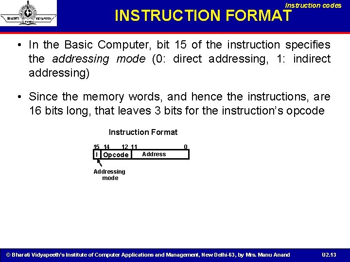
Instruction codes INSTRUCTION FORMAT • In the Basic Computer, bit 15 of the instruction specifies the addressing mode (0: direct addressing, 1: indirect addressing) • Since the memory words, and hence the instructions, are 16 bits long, that leaves 3 bits for the instruction’s opcode Instruction Format 15 14 12 11 Address I Opcode 0 Addressing mode © Bharati Vidyapeeth’s Institute of Computer Applications and Management, New Delhi-63, by Mrs. Manu Anand U 2. 13
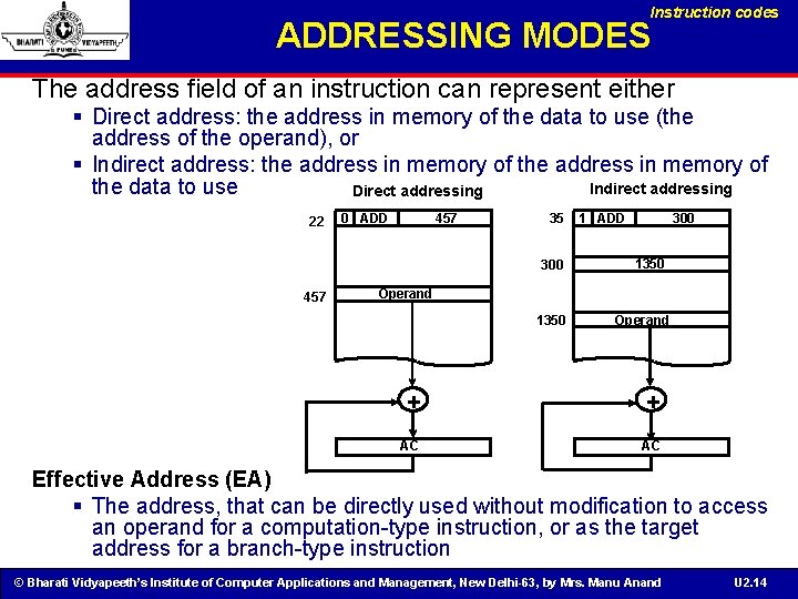
Instruction codes ADDRESSING MODES The address field of an instruction can represent either § Direct address: the address in memory of the data to use (the address of the operand), or § Indirect address: the address in memory of the data to use Indirect addressing Direct addressing 22 0 ADD 457 35 300 457 1 ADD 300 1350 Operand + + AC AC Effective Address (EA) § The address, that can be directly used without modification to access an operand for a computation-type instruction, or as the target address for a branch-type instruction © Bharati Vidyapeeth’s Institute of Computer Applications and Management, New Delhi-63, by Mrs. Manu Anand U 2. 14
Instruction codes PROCESSOR REGISTERS • A processor has many registers to hold instructions, addresses, data, etc • The processor has a register, the Program Counter (PC) that holds the memory address of the next instruction to get § Since the memory in the Basic Computer only has 4096 locations, the PC only needs 12 bits • In a direct or indirect addressing, the processor needs to keep track of what locations in memory it is addressing: The Address Register (AR) is used for this § The AR is a 12 bit register in the Basic Computer • When an operand is found, using either direct or indirect addressing, it is placed in the Data Register (DR). The processor then uses this value as data for its operation • The Basic Computer has a single general purpose register – the Accumulator (AC) © Bharati Vidyapeeth’s Institute of Computer Applications and Management, New Delhi-63, by Mrs. Manu Anand U 2. 15
Instruction codes PROCESSOR REGISTERS • The significance of a general purpose register is that it can be referred to in instructions § e. g. load AC with the contents of a specific memory location; store the contents of AC into a specified memory location • Often a processor will need a scratch register to store intermediate results or other temporary data; in the Basic Computer this is the Temporary Register (TR) • The Basic Computer uses a very simple model of input/output (I/O) operations § Input devices are considered to send 8 bits of character data to the processor § The processor can send 8 bits of character data to output devices © Bharati Vidyapeeth’s Institute of Computer Applications and Management, New Delhi-63, by Mrs. Manu Anand U 2. 16
PROCESSOR REGISTERS • The Input Register (INPR) holds an 8 bit character gotten from an input device • The Output Register (OUTR) holds an 8 bit character to be send to an output device © Bharati Vidyapeeth’s Institute of Computer Applications and Management, New Delhi-63, by Mrs. Manu Anand U 2. 17
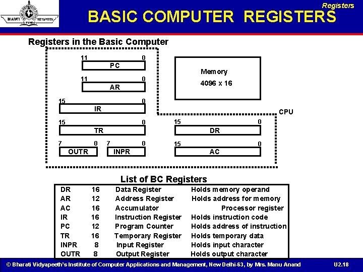
Registers BASIC COMPUTER REGISTERS Registers in the Basic Computer 11 0 PC Memory 11 0 4096 x 16 AR 15 0 IR CPU 15 0 TR 7 0 OUTR DR 7 0 15 0 INPR AC List of BC Registers DR AR AC IR PC TR INPR OUTR 16 12 16 8 8 Data Register Address Register Accumulator Instruction Register Program Counter Temporary Register Input Register Output Register Holds memory operand Holds address for memory Processor register Holds instruction code Holds address of instruction Holds temporary data Holds input character Holds output character © Bharati Vidyapeeth’s Institute of Computer Applications and Management, New Delhi-63, by Mrs. Manu Anand U 2. 18
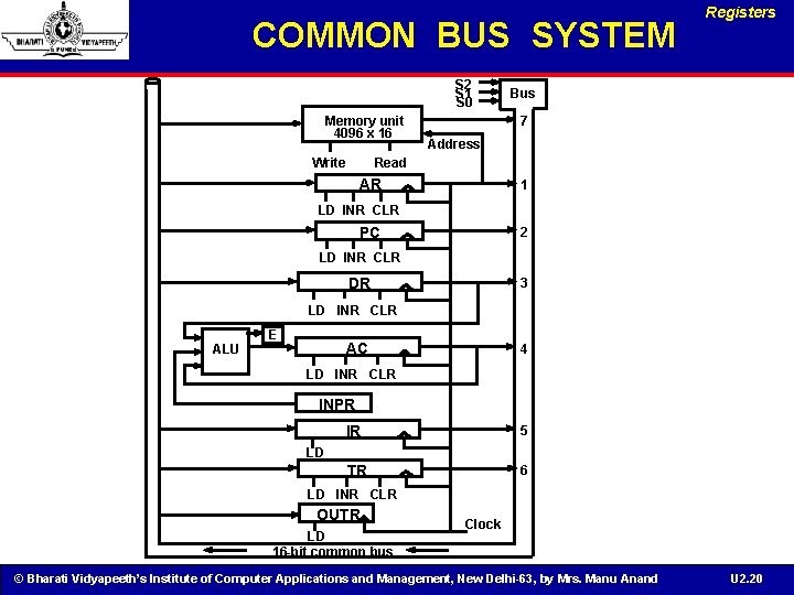
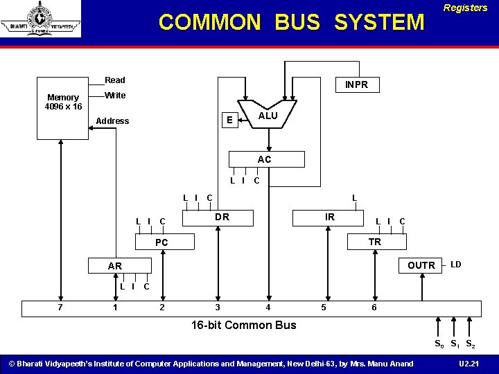
COMMON BUS SYSTEM Registers • The registers in the Basic Computer are connected using a bus • This gives a savings in circuitry over complete connections between registers © Bharati Vidyapeeth’s Institute of Computer Applications and Management, New Delhi-63, by Mrs. Manu Anand U 2. 19
COMMON BUS SYSTEM S 2 S 1 S 0 Memory unit 4096 x 16 Write Registers Bus 7 Address Read AR 1 LD INR CLR PC 2 LD INR CLR DR 3 LD INR CLR ALU E AC 4 LD INR CLR INPR IR 5 TR 6 LD LD INR CLR OUTR LD 16 -bit common bus Clock © Bharati Vidyapeeth’s Institute of Computer Applications and Management, New Delhi-63, by Mrs. Manu Anand U 2. 20
COMMON BUS SYSTEM Read Memory 4096 x 16 Registers INPR Write E Address ALU AC L I L I C C C L DR IR L I TR PC OUTR AR L I 7 1 C LD C 2 3 4 5 6 16 -bit Common Bus S 0 S 1 S 2 © Bharati Vidyapeeth’s Institute of Computer Applications and Management, New Delhi-63, by Mrs. Manu Anand U 2. 21
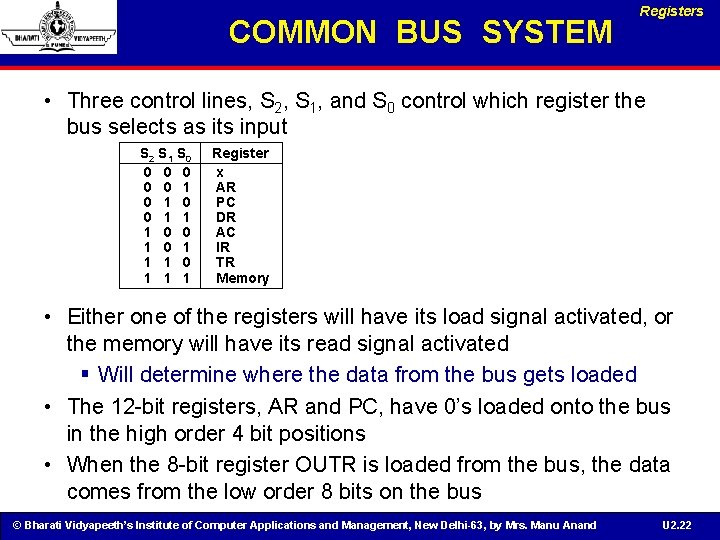
COMMON BUS SYSTEM Registers • Three control lines, S 2, S 1, and S 0 control which register the bus selects as its input S 2 S 1 S 0 0 0 1 1 1 0 0 1 1 1 Register x AR PC DR AC IR TR Memory • Either one of the registers will have its load signal activated, or the memory will have its read signal activated § Will determine where the data from the bus gets loaded • The 12 -bit registers, AR and PC, have 0’s loaded onto the bus in the high order 4 bit positions • When the 8 -bit register OUTR is loaded from the bus, the data comes from the low order 8 bits on the bus © Bharati Vidyapeeth’s Institute of Computer Applications and Management, New Delhi-63, by Mrs. Manu Anand U 2. 22
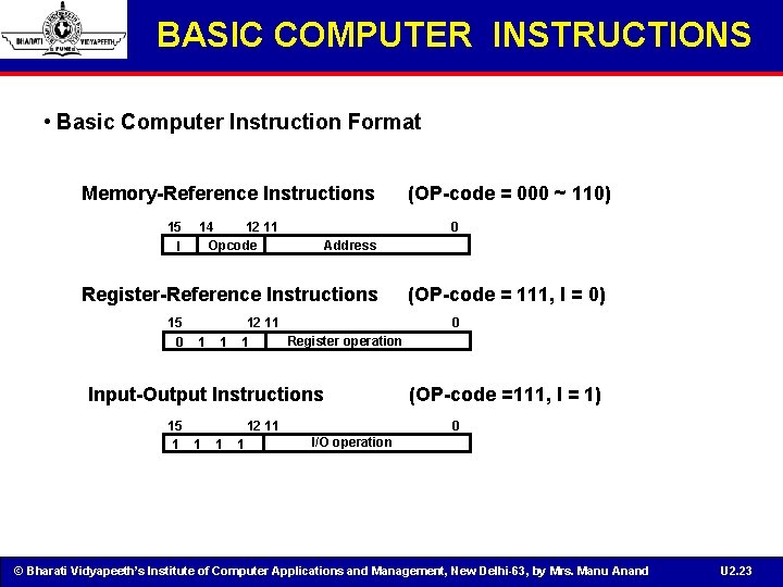
BASIC COMPUTER INSTRUCTIONS • Basic Computer Instruction Format Memory-Reference Instructions 15 I 14 12 11 Opcode 0 Address Register-Reference Instructions 15 0 1 1 12 11 Register operation 1 Input-Output Instructions 15 1 1 12 11 1 1 (OP-code = 000 ~ 110) (OP-code = 111, I = 0) 0 (OP-code =111, I = 1) 0 I/O operation © Bharati Vidyapeeth’s Institute of Computer Applications and Management, New Delhi-63, by Mrs. Manu Anand U 2. 23
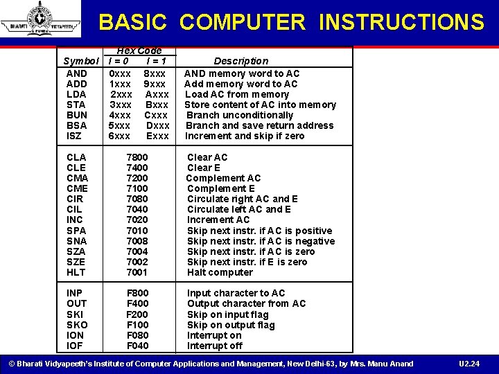
BASIC COMPUTER INSTRUCTIONS Hex Code I=0 I=1 0 xxx 8 xxx 1 xxx 9 xxx 2 xxx Axxx 3 xxx Bxxx 4 xxx Cxxx 5 xxx Dxxx 6 xxx Exxx Description AND memory word to AC Add memory word to AC Load AC from memory Store content of AC into memory Branch unconditionally Branch and save return address Increment and skip if zero CLA CLE CMA CME CIR CIL INC SPA SNA SZE HLT 7800 7400 7200 7100 7080 7040 7020 7010 7008 7004 7002 7001 Clear AC Clear E Complement AC Complement E Circulate right AC and E Circulate left AC and E Increment AC Skip next instr. if AC is positive Skip next instr. if AC is negative Skip next instr. if AC is zero Skip next instr. if E is zero Halt computer INP OUT SKI SKO ION IOF F 800 F 400 F 200 F 100 F 080 F 040 Input character to AC Output character from AC Skip on input flag Skip on output flag Interrupt on Interrupt off Symbol AND ADD LDA STA BUN BSA ISZ © Bharati Vidyapeeth’s Institute of Computer Applications and Management, New Delhi-63, by Mrs. Manu Anand U 2. 24
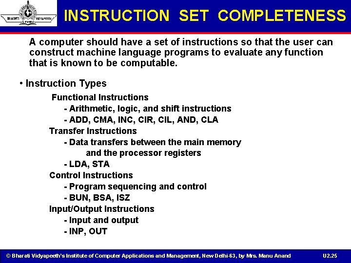
INSTRUCTION SET COMPLETENESS A computer should have a set of instructions so that the user can construct machine language programs to evaluate any function that is known to be computable. • Instruction Types Functional Instructions - Arithmetic, logic, and shift instructions - ADD, CMA, INC, CIR, CIL, AND, CLA Transfer Instructions - Data transfers between the main memory and the processor registers - LDA, STA Control Instructions - Program sequencing and control - BUN, BSA, ISZ Input/Output Instructions - Input and output - INP, OUT © Bharati Vidyapeeth’s Institute of Computer Applications and Management, New Delhi-63, by Mrs. Manu Anand U 2. 25
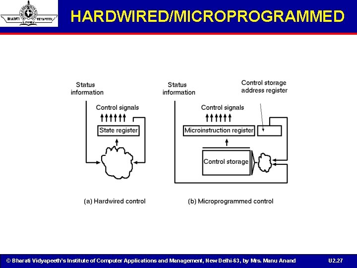
CONTROL UNIT • Control unit (CU) of a processor translates from machine instructions to the control signals for the microoperations that implement them • Control units are implemented in one of two ways • Hardwired Control § CU is made up of sequential and combinational circuits to generate the control signals • Microprogrammed Control § A control memory on the processor contains microprograms that activate the necessary control signals • We will consider a hardwired implementation of the control unit for the Basic Computer © Bharati Vidyapeeth’s Institute of Computer Applications and Management, New Delhi-63, by Mrs. Manu Anand U 2. 26
HARDWIRED/MICROPROGRAMMED © Bharati Vidyapeeth’s Institute of Computer Applications and Management, New Delhi-63, by Mrs. Manu Anand U 2. 27
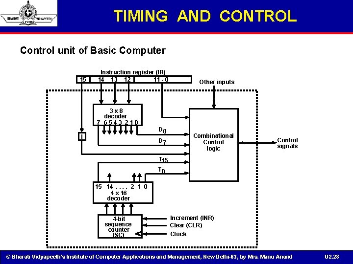
TIMING AND CONTROL Control unit of Basic Computer 15 Instruction register (IR) 14 13 12 11 - 0 Other inputs 3 x 8 decoder 7 6543 210 D 0 I D 7 Combinational Control logic Control signals T 15 T 0 15 14. . 2 1 0 4 x 16 decoder 4 -bit sequence counter (SC) Increment (INR) Clear (CLR) Clock © Bharati Vidyapeeth’s Institute of Computer Applications and Management, New Delhi-63, by Mrs. Manu Anand U 2. 28
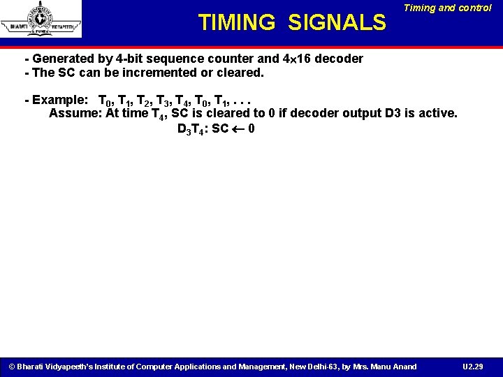
TIMING SIGNALS Timing and control - Generated by 4 -bit sequence counter and 4 16 decoder - The SC can be incremented or cleared. - Example: T 0, T 1, T 2, T 3, T 4, T 0, T 1, . . . Assume: At time T 4, SC is cleared to 0 if decoder output D 3 is active. D 3 T 4: SC 0 © Bharati Vidyapeeth’s Institute of Computer Applications and Management, New Delhi-63, by Mrs. Manu Anand U 2. 29
INSTRUCTION CYCLE • In Basic Computer, a machine instruction is executed in the following cycle: – Fetch an instruction from memory – Decode the instruction – Read the effective address from memory if the instruction has an indirect address – Execute the instruction • • After an instruction is executed, the cycle starts again at step 1, for the next instruction Note: Every different processor has its own (different) instruction cycle © Bharati Vidyapeeth’s Institute of Computer Applications and Management, New Delhi-63, by Mrs. Manu Anand U 2. 30
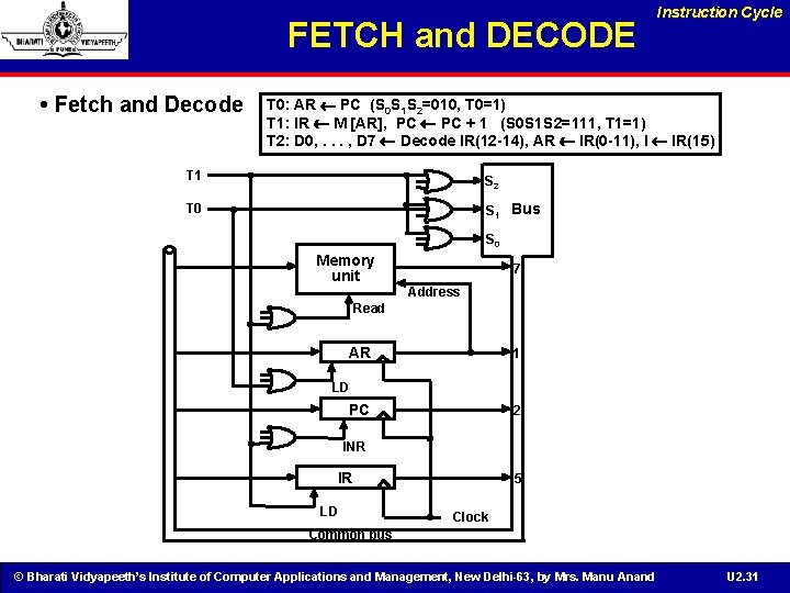
FETCH and DECODE • Fetch and Decode Instruction Cycle T 0: AR PC (S 0 S 1 S 2=010, T 0=1) T 1: IR M [AR], PC + 1 (S 0 S 1 S 2=111, T 1=1) T 2: D 0, . . . , D 7 Decode IR(12 -14), AR IR(0 -11), I IR(15) T 1 S 2 T 0 S 1 Bus S 0 Memory unit 7 Address Read AR 1 LD PC 2 INR IR LD 5 Clock Common bus © Bharati Vidyapeeth’s Institute of Computer Applications and Management, New Delhi-63, by Mrs. Manu Anand U 2. 31
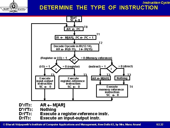
Instruction Cycle DETERMINE THE TYPE OF INSTRUCTION Start SC 0 AR PC T 0 IR M[AR], PC + 1 T 2 Decode Opcode in IR(12 -14), AR IR(0 -11), I IR(15) (Register or I/O) = 1 (I/O) = 1 I T 3 Execute input-output instruction SC 0 D'7 IT 3: D'7 I'T 3: D 7 IT 3: D 7 = 0 (Memory-reference) = 0 (register) (indirect) = 1 T 3 Execute register-reference instruction SC 0 T 3 AR M[AR] I = 0 (direct) T 3 Nothing Execute memory-reference instruction SC 0 T 4 AR M[AR] Nothing Execute a register-reference instr. Execute an input-output instr. © Bharati Vidyapeeth’s Institute of Computer Applications and Management, New Delhi-63, by Mrs. Manu Anand U 2. 32
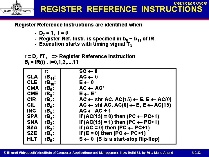
Instruction Cycle REGISTER REFERENCE INSTRUCTIONS Register Reference Instructions are identified when - D 7 = 1, I = 0 - Register Ref. Instr. is specified in b 0 ~ b 11 of IR - Execution starts with timing signal T 3 r = D 7 I T 3 => Register Reference Instruction Bi = IR(i) , i=0, 1, 2, . . . , 11 CLA CLE CMA CME CIR CIL INC SPA SNA SZE HLT r: r. B 11: r. B 10: r. B 9: r. B 8: r. B 7: r. B 6: r. B 5: r. B 4: r. B 3: r. B 2: r. B 1: r. B 0: SC 0 AC 0 E 0 AC AC’ E E’ AC shr AC, AC(15) E, E AC(0) AC shl AC, AC(0) E, E AC(15) AC + 1 if (AC(15) = 0) then (PC PC+1) if (AC(15) = 1) then (PC PC+1) if (AC = 0) then (PC PC+1) if (E = 0) then (PC PC+1) S 0 (S is a start-stop flip-flop) © Bharati Vidyapeeth’s Institute of Computer Applications and Management, New Delhi-63, by Mrs. Manu Anand U 2. 33
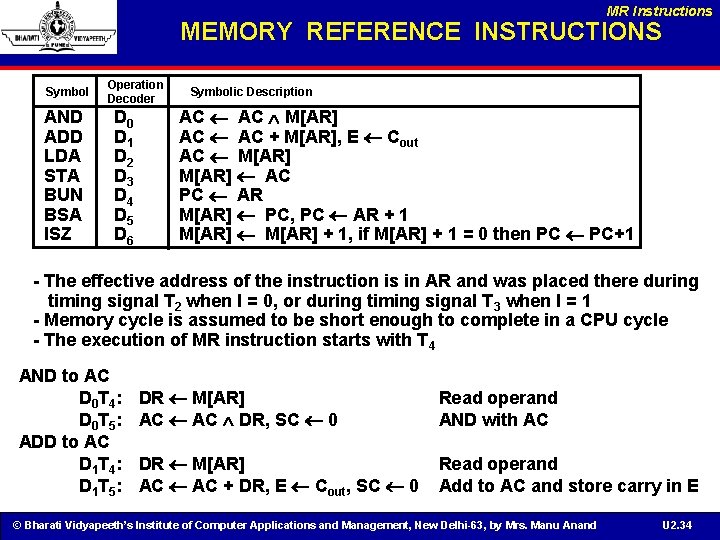
MR Instructions MEMORY REFERENCE INSTRUCTIONS Symbol AND ADD LDA STA BUN BSA ISZ Operation Decoder D 0 D 1 D 2 D 3 D 4 D 5 D 6 Symbolic Description AC M[AR] AC + M[AR], E Cout AC M[AR] AC PC AR M[AR] PC, PC AR + 1 M[AR] + 1, if M[AR] + 1 = 0 then PC PC+1 - The effective address of the instruction is in AR and was placed there during timing signal T 2 when I = 0, or during timing signal T 3 when I = 1 - Memory cycle is assumed to be short enough to complete in a CPU cycle - The execution of MR instruction starts with T 4 AND to AC D 0 T 4 : D 0 T 5 : ADD to AC D 1 T 4 : D 1 T 5 : DR M[AR] AC DR, SC 0 Read operand AND with AC DR M[AR] AC + DR, E Cout, SC 0 Read operand Add to AC and store carry in E © Bharati Vidyapeeth’s Institute of Computer Applications and Management, New Delhi-63, by Mrs. Manu Anand U 2. 34
![MEMORY REFERENCE INSTRUCTIONS LDA: Load to AC D 2 T 4: DR M[AR] D MEMORY REFERENCE INSTRUCTIONS LDA: Load to AC D 2 T 4: DR M[AR] D](http://slidetodoc.com/presentation_image/2aebcd7b1150f232858b7e02efb90c0c/image-35.jpg)
MEMORY REFERENCE INSTRUCTIONS LDA: Load to AC D 2 T 4: DR M[AR] D 2 T 5: AC DR, SC 0 STA: Store AC D 3 T 4: M[AR] AC, SC 0 BUN: Branch Unconditionally D 4 T 4: PC AR, SC 0 BSA: Branch and Save Return Address M[AR] PC, PC AR + 1 Memory, PC, AR at time T 4 20 PC = 21 0 BSA 135 Next instruction AR = 135 136 Subroutine 1 BUN Memory 135 Memory, PC after execution 20 0 BSA 135 21 Next instruction 135 21 Subroutine PC = 136 1 BUN 135 Memory © Bharati Vidyapeeth’s Institute of Computer Applications and Management, New Delhi-63, by Mrs. Manu Anand U 2. 35
![MR Instructions MEMORY REFERENCE INSTRUCTIONS BSA: D 5 T 4: M[AR] PC, AR + MR Instructions MEMORY REFERENCE INSTRUCTIONS BSA: D 5 T 4: M[AR] PC, AR +](http://slidetodoc.com/presentation_image/2aebcd7b1150f232858b7e02efb90c0c/image-36.jpg)
MR Instructions MEMORY REFERENCE INSTRUCTIONS BSA: D 5 T 4: M[AR] PC, AR + 1 D 5 T 5: PC AR, SC 0 ISZ: Increment and Skip-if-Zero D 6 T 4: DR M[AR] D 6 T 5: DR + 1 D 6 T 4: M[AR] DR, if (DR = 0) then (PC PC + 1), SC 0 © Bharati Vidyapeeth’s Institute of Computer Applications and Management, New Delhi-63, by Mrs. Manu Anand U 2. 36
![FLOWCHART FOR MEMORY REFERENCE INSTRUCTIONS Memory-reference instruction AND D 0 T 4 DR M[AR] FLOWCHART FOR MEMORY REFERENCE INSTRUCTIONS Memory-reference instruction AND D 0 T 4 DR M[AR]](http://slidetodoc.com/presentation_image/2aebcd7b1150f232858b7e02efb90c0c/image-37.jpg)
FLOWCHART FOR MEMORY REFERENCE INSTRUCTIONS Memory-reference instruction AND D 0 T 4 DR M[AR] ADD LDA D 1 T 4 DR M[AR] D 0 T 5 D 1 T 5 AC DR AC + DR SC 0 E Cout SC 0 BUN BSA STA D 2 T 4 DR M[AR] D 3 T 4 M[AR] AC SC 0 D 2 T 5 AC DR SC 0 ISZ D 4 T 4 D 5 T 4 D 6 T 4 PC AR M[AR] PC DR M[AR] SC 0 AR + 1 D 5 T 5 PC AR SC 0 D 6 T 5 DR + 1 D 6 T 6 M[AR] DR If (DR = 0) then (PC PC + 1) SC 0 © Bharati Vidyapeeth’s Institute of Computer Applications and Management, New Delhi-63, by Mrs. Manu Anand U 2. 37
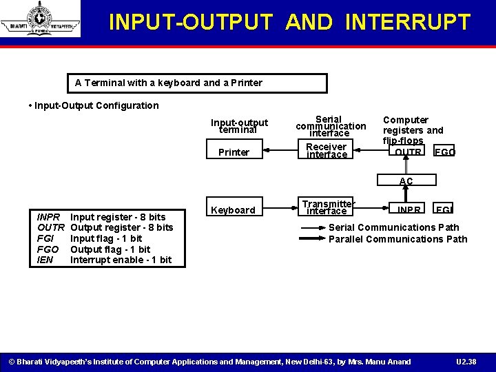
INPUT-OUTPUT AND INTERRUPT A Terminal with a keyboard and a Printer • Input-Output Configuration Input-output terminal Printer Serial communication interface Receiver interface Computer registers and flip-flops OUTR FGO AC INPR OUTR FGI FGO IEN Input register - 8 bits Output register - 8 bits Input flag - 1 bit Output flag - 1 bit Interrupt enable - 1 bit Keyboard Transmitter interface INPR FGI Serial Communications Path Parallel Communications Path © Bharati Vidyapeeth’s Institute of Computer Applications and Management, New Delhi-63, by Mrs. Manu Anand U 2. 38
INPUT-OUTPUT AND INTERRUPT - The terminal sends and receives serial information - The serial info. from the keyboard is shifted into INPR -The serial info. for the printer is stored in the OUTR - INPR and OUTR communicate with the terminal serially and with the AC in parallel. - The flags are needed to synchronize the timing difference between I/O device and the computer © Bharati Vidyapeeth’s Institute of Computer Applications and Management, New Delhi-63, by Mrs. Manu Anand U 2. 39
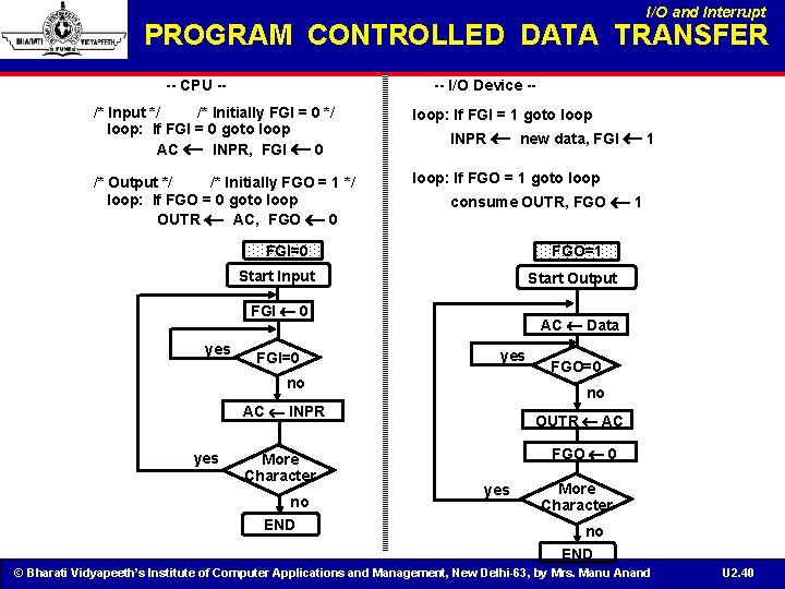
I/O and Interrupt PROGRAM CONTROLLED DATA TRANSFER -- CPU -- -- I/O Device -- /* Input */ /* Initially FGI = 0 */ loop: If FGI = 0 goto loop AC INPR, FGI 0 loop: If FGI = 1 goto loop /* Output */ /* Initially FGO = 1 */ loop: If FGO = 0 goto loop OUTR AC, FGO 0 loop: If FGO = 1 goto loop INPR new data, FGI 1 consume OUTR, FGO 1 FGI=0 FGO=1 Start Input Start Output FGI 0 yes FGI=0 AC Data yes no no AC INPR yes More Character no END FGO=0 OUTR AC FGO 0 yes More Character no END © Bharati Vidyapeeth’s Institute of Computer Applications and Management, New Delhi-63, by Mrs. Manu Anand U 2. 40
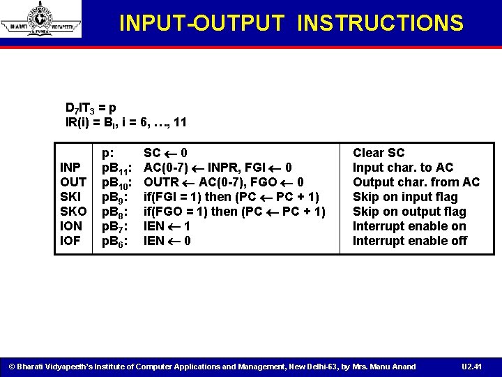
INPUT-OUTPUT INSTRUCTIONS D 7 IT 3 = p IR(i) = Bi, i = 6, …, 11 INP OUT SKI SKO ION IOF p: p. B 11: p. B 10: p. B 9: p. B 8: p. B 7: p. B 6: SC 0 AC(0 -7) INPR, FGI 0 OUTR AC(0 -7), FGO 0 if(FGI = 1) then (PC PC + 1) if(FGO = 1) then (PC PC + 1) IEN 1 IEN 0 Clear SC Input char. to AC Output char. from AC Skip on input flag Skip on output flag Interrupt enable on Interrupt enable off © Bharati Vidyapeeth’s Institute of Computer Applications and Management, New Delhi-63, by Mrs. Manu Anand U 2. 41
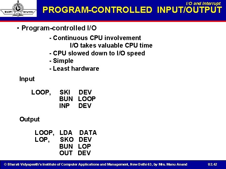
I/O and Interrupt PROGRAM-CONTROLLED INPUT/OUTPUT • Program-controlled I/O - Continuous CPU involvement I/O takes valuable CPU time - CPU slowed down to I/O speed - Simple - Least hardware Input LOOP, SKI DEV BUN LOOP INP DEV Output LOOP, LDA DATA LOP, SKO DEV BUN LOP OUT DEV © Bharati Vidyapeeth’s Institute of Computer Applications and Management, New Delhi-63, by Mrs. Manu Anand U 2. 42
INTERRUPT INITIATED INPUT/OUTPUT - Open communication only when some data has to be passed --> interrupt. - The I/O interface, instead of the CPU, monitors the I/O device. - When the interface founds that the I/O device is ready for data transfer, it generates an interrupt request to the CPU - Upon detecting an interrupt, the CPU stops momentarily the task it is doing, branches to the service routine to process the data transfer, and then returns to the task it was performing. * IEN (Interrupt-enable flip-flop) - can be set and cleared by instructions - when cleared, the computer cannot be interrupted © Bharati Vidyapeeth’s Institute of Computer Applications and Management, New Delhi-63, by Mrs. Manu Anand U 2. 43
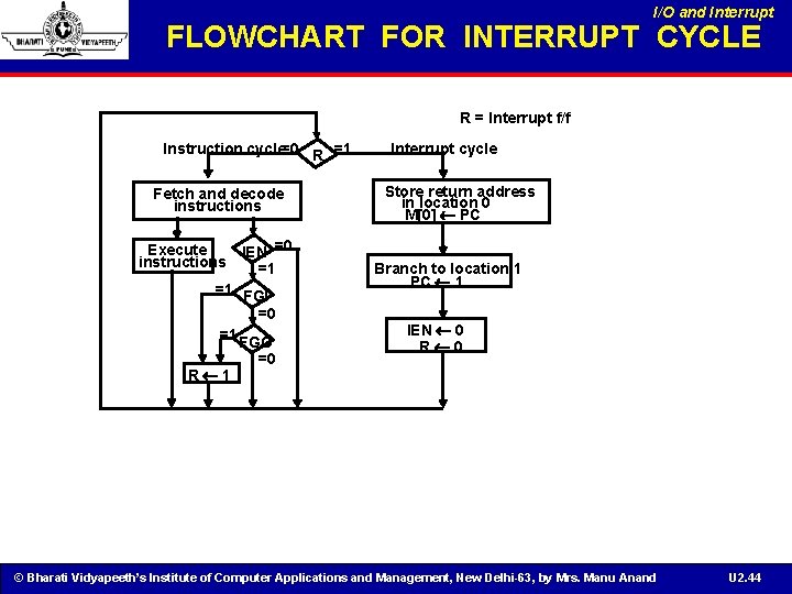
I/O and Interrupt FLOWCHART FOR INTERRUPT CYCLE R = Interrupt f/f Instruction cycle=0 R =1 Fetch and decode instructions Execute IEN =0 instructions =1 =1 FGI =0 =1 FGO R 1 =0 Interrupt cycle Store return address in location 0 M[0] PC Branch to location 1 PC 1 IEN 0 R 0 © Bharati Vidyapeeth’s Institute of Computer Applications and Management, New Delhi-63, by Mrs. Manu Anand U 2. 44
INTERRUPT CYCLE I/O and Interrupt - The interrupt cycle is a HW implementation of a branch and save return address operation. - At the beginning of the next instruction cycle, the instruction that is read from memory is in address 1. -At memory address 1, the programmer must store a branch instruction that sends the control to an interrupt service routine - The instruction that returns the control to the original program is "indirect BUN 0" © Bharati Vidyapeeth’s Institute of Computer Applications and Management, New Delhi-63, by Mrs. Manu Anand U 2. 45
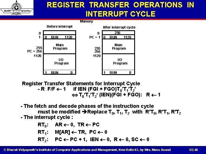
REGISTER TRANSFER OPERATIONS IN INTERRUPT CYCLE Memory Before interrupt 0 1 0 BUN 1120 Main Program 255 PC = 256 1120 After interrupt cycle 0 PC = 1 0 Main Program 255 256 1120 I/O Program 1 BUN 256 BUN 1120 I/O Program 0 1 BUN 0 Register Transfer Statements for Interrupt Cycle - R F/F 1 if IEN (FGI + FGO)T 0 T 1 T 2 (IEN)(FGI + FGO): R 1 - The fetch and decode phases of the instruction cycle must be modified Replace T 0, T 1, T 2 with R'T 0, R'T 1, R'T 2 - The interrupt cycle : RT 0: AR 0, TR PC RT 1: M[AR] TR, PC 0 RT 2: PC + 1, IEN 0, R 0, SC 0 © Bharati Vidyapeeth’s Institute of Computer Applications and Management, New Delhi-63, by Mrs. Manu Anand U 2. 46
I/O and Interrupt FURTHER QUESTIONS ON INTERRUPT • How can the CPU recognize the device requesting an interrupt ? • Since different devices are likely to require different interrupt service routines, how can the CPU obtain the starting address of the appropriate routine in each case ? • Should any device be allowed to interrupt the CPU while another interrupt is being serviced ? • How can the situation be handled when two or more interrupt requests occur simultaneously ? © Bharati Vidyapeeth’s Institute of Computer Applications and Management, New Delhi-63, by Mrs. Manu Anand U 2. 47
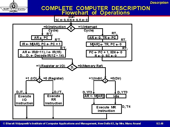
Description COMPLETE COMPUTER DESCRIPTION Flowchart of Operations start SC 0, IEN 0, R 0 =0(Instruction R Cycle) R’T 0 AR PC R’T 1 IR M[AR], PC + 1 R’T 2 AR IR(0~11), I IR(15) D 0. . . D 7 Decode IR(12 ~ 14) =1(Register or I/O) =1 (I/O) D 7 IT 3 Execute I/O Instruction I =0 (Register) D 7 I’T 3 Execute RR Instruction D 7 =1(Interrupt Cycle) RT 0 AR 0, TR PC RT 1 M[AR] TR, PC 0 RT 2 PC + 1, IEN 0 R 0, SC 0 =0(Memory Ref) =1(Indir) D 7’IT 3 AR <- M[AR] I =0(Dir) D 7’I’T 3 Idle Execute MR Instruction D 7’T 4 © Bharati Vidyapeeth’s Institute of Computer Applications and Management, New Delhi-63, by Mrs. Manu Anand U 2. 48
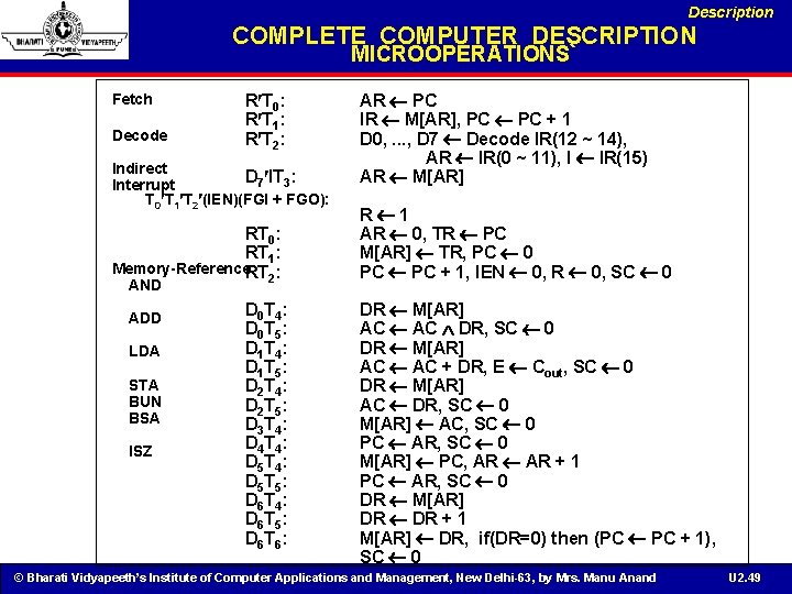
Description COMPLETE COMPUTER DESCRIPTION MICROOPERATIONS` Fetch Decode R T 0: R T 1: R T 2: Indirect D 7 IT 3: Interrupt T 0 T 1 T 2 (IEN)(FGI + FGO): RT 0: RT 1: Memory-Reference. RT : 2 AND ADD LDA STA BUN BSA ISZ D 0 T 4 : D 0 T 5 : D 1 T 4 : D 1 T 5 : D 2 T 4 : D 2 T 5 : D 3 T 4 : D 4 T 4 : D 5 T 5 : D 6 T 4 : D 6 T 5 : D 6 T 6 : AR PC IR M[AR], PC + 1 D 0, . . . , D 7 Decode IR(12 ~ 14), AR IR(0 ~ 11), I IR(15) AR M[AR] R 1 AR 0, TR PC M[AR] TR, PC 0 PC + 1, IEN 0, R 0, SC 0 DR M[AR] AC DR, SC 0 DR M[AR] AC + DR, E Cout, SC 0 DR M[AR] AC DR, SC 0 M[AR] AC, SC 0 PC AR, SC 0 M[AR] PC, AR + 1 PC AR, SC 0 DR M[AR] DR + 1 M[AR] DR, if(DR=0) then (PC PC + 1), SC 0 © Bharati Vidyapeeth’s Institute of Computer Applications and Management, New Delhi-63, by Mrs. Manu Anand U 2. 49
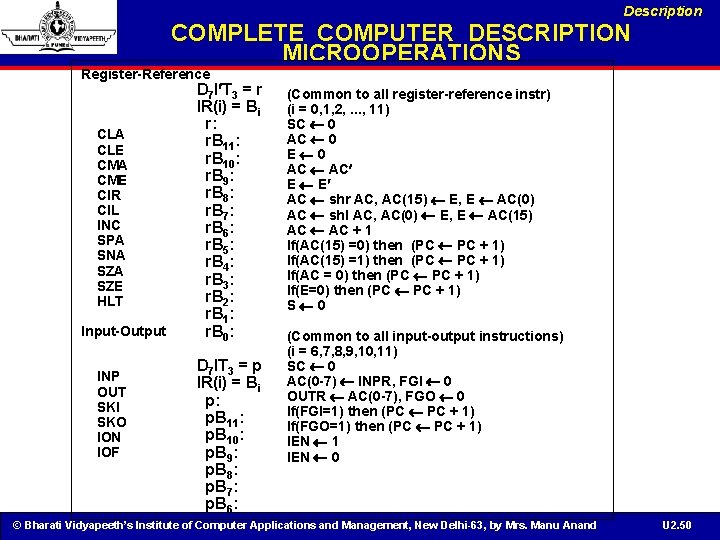
Description COMPLETE COMPUTER DESCRIPTION MICROOPERATIONS Register-Reference CLA CLE CMA CME CIR CIL INC SPA SNA SZE HLT Input-Output INP OUT SKI SKO ION IOF D 7 I T 3 = r IR(i) = Bi r: r. B 11: r. B 10: r. B 9: r. B 8: r. B 7: r. B 6: r. B 5: r. B 4: r. B 3: r. B 2: r. B 1: r. B 0: D 7 IT 3 = p IR(i) = Bi p: p. B 11: p. B 10: p. B 9: p. B 8: p. B 7: p. B 6: (Common to all register-reference instr) (i = 0, 1, 2, . . . , 11) SC 0 AC 0 E 0 AC E E AC shr AC, AC(15) E, E AC(0) AC shl AC, AC(0) E, E AC(15) AC + 1 If(AC(15) =0) then (PC PC + 1) If(AC(15) =1) then (PC PC + 1) If(AC = 0) then (PC PC + 1) If(E=0) then (PC PC + 1) S 0 (Common to all input-output instructions) (i = 6, 7, 8, 9, 10, 11) SC 0 AC(0 -7) INPR, FGI 0 OUTR AC(0 -7), FGO 0 If(FGI=1) then (PC PC + 1) If(FGO=1) then (PC PC + 1) IEN 1 IEN 0 © Bharati Vidyapeeth’s Institute of Computer Applications and Management, New Delhi-63, by Mrs. Manu Anand U 2. 50
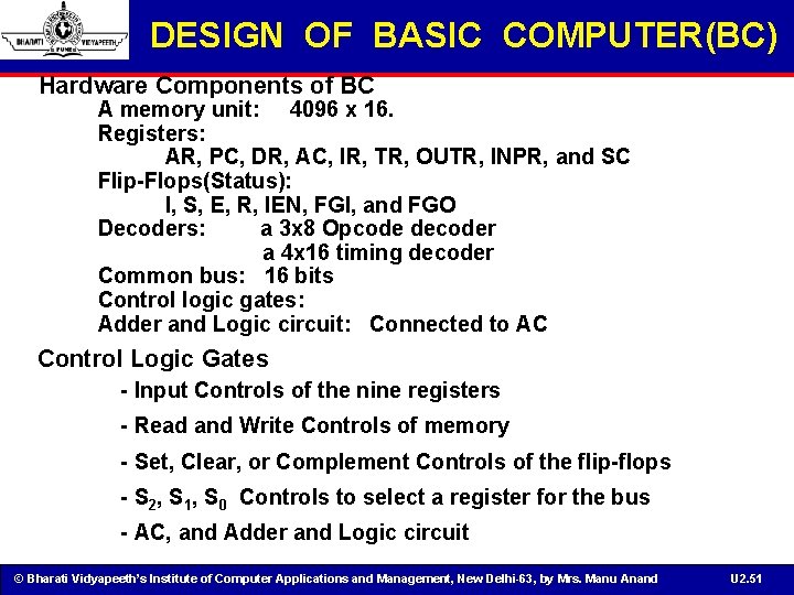
DESIGN OF BASIC COMPUTER(BC) Hardware Components of BC A memory unit: 4096 x 16. Registers: AR, PC, DR, AC, IR, TR, OUTR, INPR, and SC Flip-Flops(Status): I, S, E, R, IEN, FGI, and FGO Decoders: a 3 x 8 Opcode decoder a 4 x 16 timing decoder Common bus: 16 bits Control logic gates: Adder and Logic circuit: Connected to AC Control Logic Gates - Input Controls of the nine registers - Read and Write Controls of memory - Set, Clear, or Complement Controls of the flip-flops - S 2, S 1, S 0 Controls to select a register for the bus - AC, and Adder and Logic circuit © Bharati Vidyapeeth’s Institute of Computer Applications and Management, New Delhi-63, by Mrs. Manu Anand U 2. 51
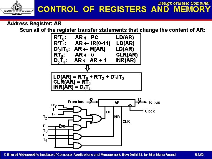
Design of Basic Computer CONTROL OF REGISTERS AND MEMORY Address Register; AR Scan all of the register transfer statements that change the content of AR: R’T 0: AR PC LD(AR) R’T 2: AR IR(0 -11) LD(AR) D’ 7 IT 3: AR M[AR] LD(AR) RT 0: AR 0 CLR(AR) D 5 T 4: AR + 1 INR(AR) LD(AR) = R'T 0 + R'T 2 + D'7 IT 3 CLR(AR) = RT 0 INR(AR) = D 5 T 4 T 2 D'7 I T 3 From bus 12 12 AR To bus Clock LD INR CLR R T 0 D T 4 © Bharati Vidyapeeth’s Institute of Computer Applications and Management, New Delhi-63, by Mrs. Manu Anand U 2. 52
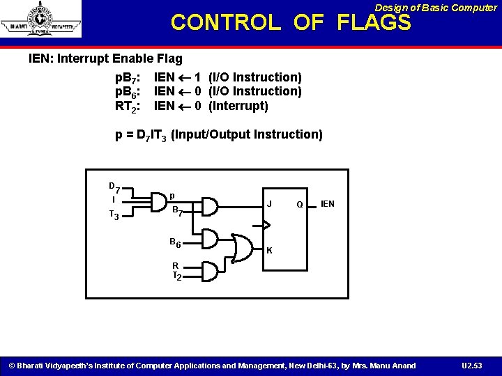
Design of Basic Computer CONTROL OF FLAGS IEN: Interrupt Enable Flag p. B 7: IEN 1 (I/O Instruction) p. B 6: IEN 0 (I/O Instruction) RT 2: IEN 0 (Interrupt) p = D 7 IT 3 (Input/Output Instruction) D I 7 T 3 p B 7 B 6 J Q IEN K R T 2 © Bharati Vidyapeeth’s Institute of Computer Applications and Management, New Delhi-63, by Mrs. Manu Anand U 2. 53
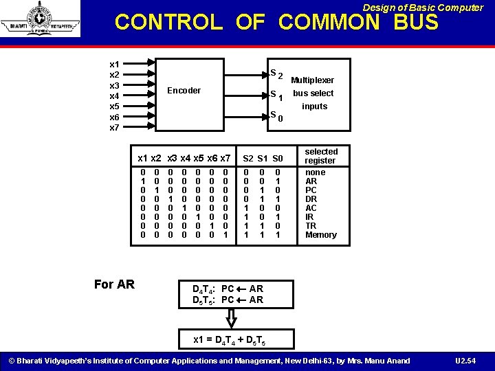
Design of Basic Computer CONTROL OF COMMON BUS x 1 x 2 x 3 x 4 x 5 x 6 x 7 S 2 Encoder S 1 S 0 x 1 x 2 x 3 x 4 x 5 x 6 x 7 0 1 0 0 0 For AR 0 0 1 0 0 0 0 0 0 0 0 1 0 0 0 0 1 S 2 S 1 S 0 0 0 1 1 0 1 0 1 Multiplexer bus select inputs selected register none AR PC DR AC IR TR Memory D 4 T 4: PC AR D 5 T 5: PC AR x 1 = D 4 T 4 + D 5 T 5 © Bharati Vidyapeeth’s Institute of Computer Applications and Management, New Delhi-63, by Mrs. Manu Anand U 2. 54
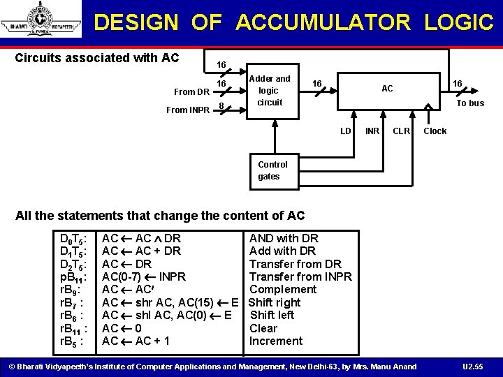
DESIGN OF ACCUMULATOR LOGIC Circuits associated with AC From DR From INPR 16 16 8 Adder and logic circuit 16 16 AC To bus LD INR CLR Clock Control gates All the statements that change the content of AC D 0 T 5 : D 1 T 5 : D 2 T 5 : p. B 11: r. B 9: r. B 7 : r. B 6 : r. B 11 : r. B 5 : AC DR AC + DR AC(0 -7) INPR AC AC shr AC, AC(15) E AC shl AC, AC(0) E AC 0 AC + 1 AND with DR Add with DR Transfer from INPR Complement Shift right Shift left Clear Increment © Bharati Vidyapeeth’s Institute of Computer Applications and Management, New Delhi-63, by Mrs. Manu Anand U 2. 55
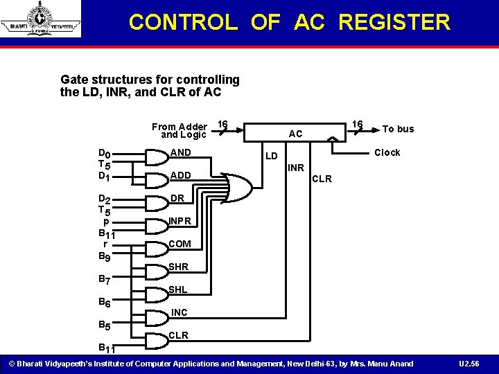
CONTROL OF AC REGISTER Gate structures for controlling the LD, INR, and CLR of AC From Adder and Logic D 0 T 5 D 1 AND D 2 T 5 p B 11 r B 9 DR B 7 B 6 B 5 ADD 16 16 AC To bus Clock LD INR CLR INPR COM SHR SHL INC CLR B 11 © Bharati Vidyapeeth’s Institute of Computer Applications and Management, New Delhi-63, by Mrs. Manu Anand U 2. 56
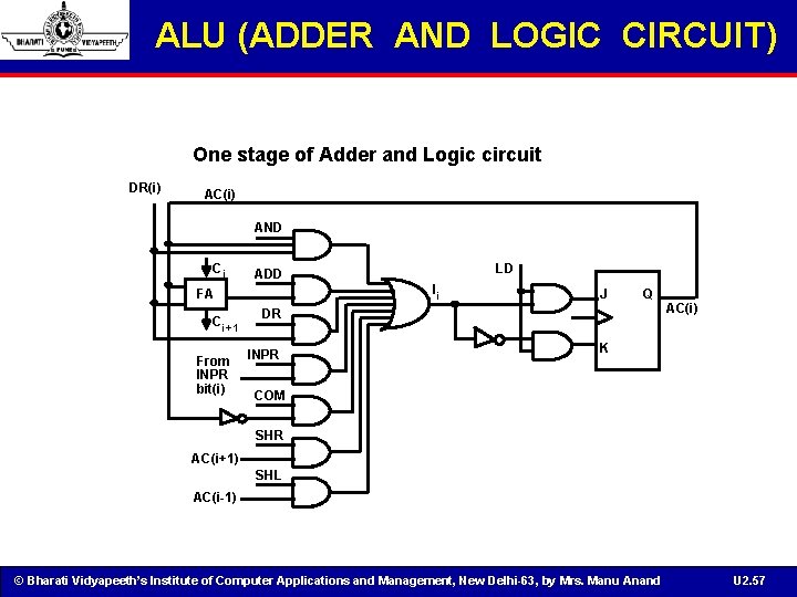
ALU (ADDER AND LOGIC CIRCUIT) One stage of Adder and Logic circuit DR(i) AC(i) AND Ci Ii FA C i+1 From INPR bit(i) LD ADD J Q DR INPR AC(i) K COM SHR AC(i+1) SHL AC(i-1) © Bharati Vidyapeeth’s Institute of Computer Applications and Management, New Delhi-63, by Mrs. Manu Anand U 2. 57
CONCLUSIONS • Designing of the instructions format • Types of Computer cycles • Design of Control Logic © Bharati Vidyapeeth’s Institute of Computer Applications and Management, New Delhi-63, by Mrs. Manu Anand U 2. 58
SUMMARY • Computer’s structure indicates its internal connections § Functional structure identifies functional block and relationship between these blocks § Physical structure identifies the physical modules and interconnection between them. • Computer function indicates the behavior. At overall level its function is program execution. • Relation between computer organization and architecture. • Design of ALU • Design of bus, its interconnection and control logic © Bharati Vidyapeeth’s Institute of Computer Applications and Management, New Delhi-63, by Mrs. Manu Anand U 2. 59
CONTROL UNIT DESIGN © Bharati Vidyapeeth’s Institute of Computer Applications and Management, New Delhi-63. , by Mrs. Manu Anand U 2. 60
LEARNING OBJECTIVES • Microprogammed Control Unit • Control Unit Design • Introduction to Pipelining © Bharati Vidyapeeth’s Institute of Computer Applications and Management, New Delhi-63, by Mrs. Manu Anand U 2. 61
MICROPROGRAMMED CONTROL • Control Memory • Sequencing Microinstructions • Microprogram Example • Design of Control Unit • Microinstruction Format • Nanostorage and Nanoprogram © Bharati Vidyapeeth’s Institute of Computer Applications and Management, New Delhi-63, by Mrs. Manu Anand U 2. 62
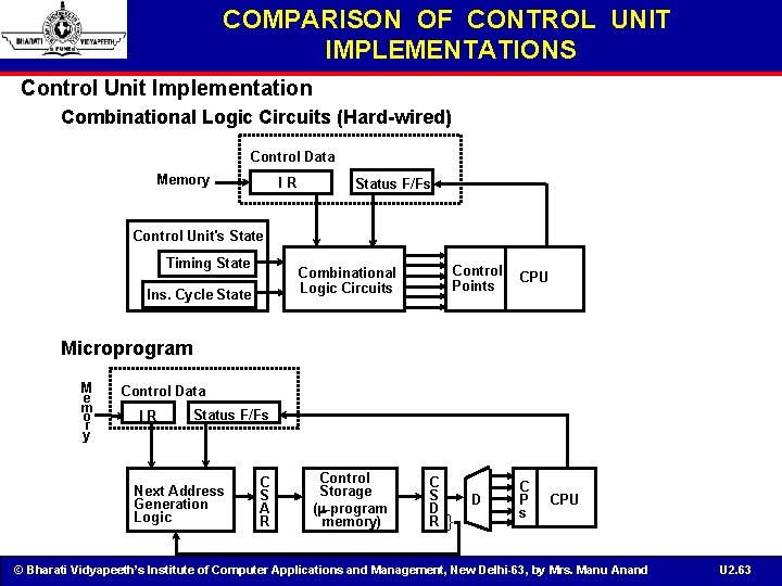
COMPARISON OF CONTROL UNIT IMPLEMENTATIONS Control Unit Implementation Combinational Logic Circuits (Hard-wired) Control Data Memory IR Status F/Fs Control Unit's State Timing State Control Points Combinational Logic Circuits Ins. Cycle State CPU Microprogram M e m o r y Control Data IR Status F/Fs Next Address Generation Logic C S A R Control Storage ( -program memory) C S D R D } C P s CPU © Bharati Vidyapeeth’s Institute of Computer Applications and Management, New Delhi-63, by Mrs. Manu Anand U 2. 63
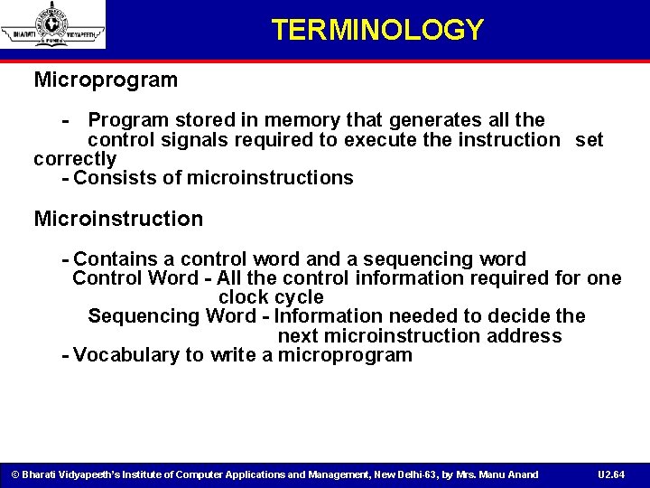
TERMINOLOGY Microprogram - Program stored in memory that generates all the control signals required to execute the instruction set correctly - Consists of microinstructions Microinstruction - Contains a control word and a sequencing word Control Word - All the control information required for one clock cycle Sequencing Word - Information needed to decide the next microinstruction address - Vocabulary to write a microprogram © Bharati Vidyapeeth’s Institute of Computer Applications and Management, New Delhi-63, by Mrs. Manu Anand U 2. 64
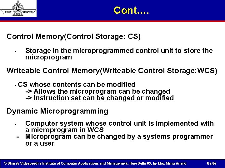
Cont…. Control Memory(Control Storage: CS) - Storage in the microprogrammed control unit to store the microprogram Writeable Control Memory(Writeable Control Storage: WCS) - CS whose contents can be modified -> Allows the microprogram can be changed -> Instruction set can be changed or modified Dynamic Microprogramming - - Computer system whose control unit is implemented with a microprogram in WCS Microprogram can be changed by a systems programmer or a user © Bharati Vidyapeeth’s Institute of Computer Applications and Management, New Delhi-63, by Mrs. Manu Anand U 2. 65
Cont… Sequencer (Microprogram Sequencer) A Microprogram Control Unit that determines the Microinstruction Address to be executed in the next clock cycle - In-line Sequencing - Branch - Conditional Branch - Subroutine - Loop - Instruction OP-code mapping © Bharati Vidyapeeth’s Institute of Computer Applications and Management, New Delhi-63, by Mrs. Manu Anand U 2. 66
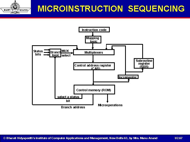
MICROINSTRUCTION SEQUENCING Instruction code Mapping logic Status bits Branch MUX logic select Multiplexers Subroutine register (SBR) Control address register (CAR) Incrementer Control memory (ROM) select a status bit Branch address Microoperations © Bharati Vidyapeeth’s Institute of Computer Applications and Management, New Delhi-63, by Mrs. Manu Anand U 2. 67
MICROINSTRUCTION SEQUENCING Sequencing Capabilities Required in a Control Storage - Incrementing of the control address register - Unconditional and conditional branches - A mapping process from the bits of the machine instruction to an address for control memory - A facility for subroutine call and return © Bharati Vidyapeeth’s Institute of Computer Applications and Management, New Delhi-63, by Mrs. Manu Anand U 2. 68
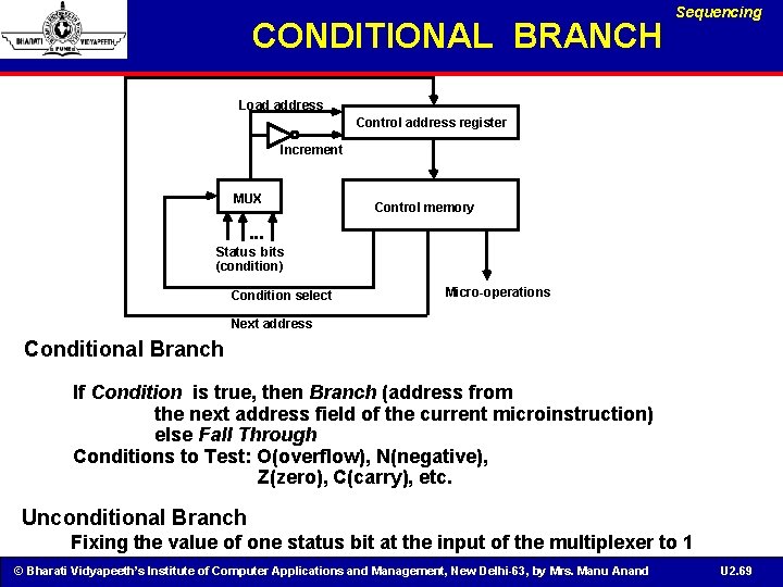
CONDITIONAL BRANCH Sequencing Load address Control address register Increment MUX Control memory . . . Status bits (condition) Condition select Micro-operations Next address Conditional Branch If Condition is true, then Branch (address from the next address field of the current microinstruction) else Fall Through Conditions to Test: O(overflow), N(negative), Z(zero), C(carry), etc. Unconditional Branch Fixing the value of one status bit at the input of the multiplexer to 1 © Bharati Vidyapeeth’s Institute of Computer Applications and Management, New Delhi-63, by Mrs. Manu Anand U 2. 69
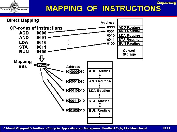
Sequencing MAPPING OF INSTRUCTIONS Direct Mapping OP-codes of Instructions ADD 0000 AND 0001 LDA 0010 STA 0011 BUN 0100 Mapping Bits 10 xxxx 010 . . . Address 0000 0001 0010 0011 0100 ADD Routine AND Routine LDA Routine STA Routine BUN Routine Control Storage Address 10 0000 010 ADD Routine 10 0001 010 AND Routine 10 0010 LDA Routine 10 0011 010 STA Routine 10 010 BUN Routine © Bharati Vidyapeeth’s Institute of Computer Applications and Management, New Delhi-63, by Mrs. Manu Anand U 2. 70
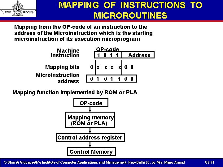
MAPPING OF INSTRUCTIONS TO MICROROUTINES Mapping from the OP-code of an instruction to the address of the Microinstruction which is the starting microinstruction of its execution microprogram Machine Instruction Mapping bits Microinstruction address OP-code 1 0 1 1 Address 0 x x 0 0 0 1 1 0 0 Mapping function implemented by ROM or PLA OP-code Mapping memory (ROM or PLA) Control address register Control Memory © Bharati Vidyapeeth’s Institute of Computer Applications and Management, New Delhi-63, by Mrs. Manu Anand U 2. 71
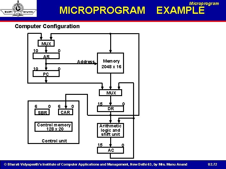
MICROPROGRAM Microprogram EXAMPLE Computer Configuration MUX 10 0 AR Address 10 0 Memory 2048 x 16 PC MUX 6 0 SBR 6 0 15 CAR Control memory 128 x 20 Control unit DR 0 Arithmetic logic and shift unit 15 0 AC © Bharati Vidyapeeth’s Institute of Computer Applications and Management, New Delhi-63, by Mrs. Manu Anand U 2. 72
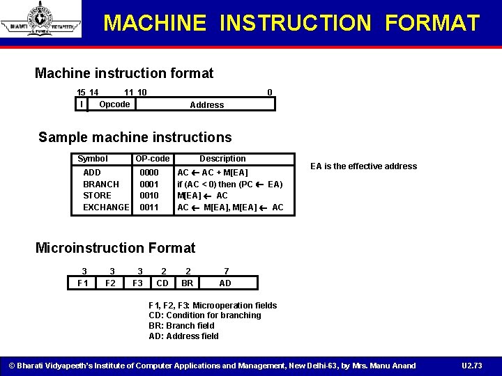
MACHINE INSTRUCTION FORMAT Machine instruction format 15 14 11 10 Opcode I 0 Address Sample machine instructions Symbol ADD BRANCH STORE EXCHANGE OP-code 0000 0001 0010 0011 Description AC + M[EA] if (AC < 0) then (PC EA) M[EA] AC AC M[EA], M[EA] AC EA is the effective address Microinstruction Format 3 F 1 3 F 2 3 F 3 2 CD 2 BR 7 AD F 1, F 2, F 3: Microoperation fields CD: Condition for branching BR: Branch field AD: Address field © Bharati Vidyapeeth’s Institute of Computer Applications and Management, New Delhi-63, by Mrs. Manu Anand U 2. 73
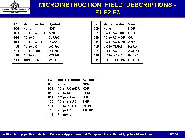
MICROINSTRUCTION FIELD DESCRIPTIONS F 1, F 2, F 3 F 1 000 001 010 011 100 101 110 111 Microoperation None AC + DR AC 0 AC + 1 AC DR AR DR(0 -10) AR PC M[AR] DR Symbol NOP ADD CLRAC INCAC DRTAR PCTAR WRITE F 3 000 001 010 011 100 101 110 111 Microoperation None AC DR AC AC’ AC shl AC AC shr AC PC + 1 PC AR Reserved F 2 000 001 010 011 100 101 110 111 Microoperation None AC - DR AC AC DR DR M[AR] DR AC DR + 1 DR(0 -10) PC Symbol NOP SUB OR AND READ ACTDR INCDR PCTDR Symbol NOP XOR COM SHL SHR INCPC ARTPC © Bharati Vidyapeeth’s Institute of Computer Applications and Management, New Delhi-63, by Mrs. Manu Anand U 2. 74
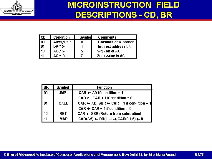
MICROINSTRUCTION FIELD DESCRIPTIONS - CD, BR CD 00 01 10 11 Condition Always = 1 DR(15) AC = 0 BR 00 Symbol JMP 01 CALL 10 11 RET MAP Symbol U I S Z Comments Unconditional branch Indirect address bit Sign bit of AC Zero value in AC Function CAR AD if condition = 1 CAR + 1 if condition = 0 CAR AD, SBR CAR + 1 if condition = 1 CAR + 1 if condition = 0 CAR SBR (Return from subroutine) CAR(2 -5) DR(11 -14), CAR(0, 1, 6) 0 © Bharati Vidyapeeth’s Institute of Computer Applications and Management, New Delhi-63, by Mrs. Manu Anand U 2. 75
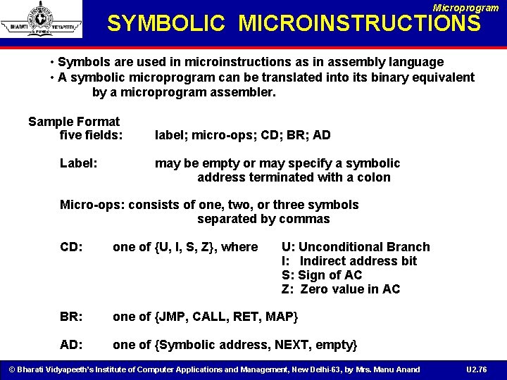
Microprogram SYMBOLIC MICROINSTRUCTIONS • Symbols are used in microinstructions as in assembly language • A symbolic microprogram can be translated into its binary equivalent by a microprogram assembler. Sample Format five fields: Label: label; micro-ops; CD; BR; AD may be empty or may specify a symbolic address terminated with a colon Micro-ops: consists of one, two, or three symbols separated by commas CD: one of {U, I, S, Z}, where U: Unconditional Branch I: Indirect address bit S: Sign of AC Z: Zero value in AC BR: one of {JMP, CALL, RET, MAP} AD: one of {Symbolic address, NEXT, empty} © Bharati Vidyapeeth’s Institute of Computer Applications and Management, New Delhi-63, by Mrs. Manu Anand U 2. 76
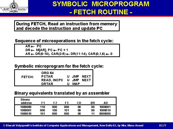
SYMBOLIC MICROPROGRAM - FETCH ROUTINE During FETCH, Read an instruction from memory and decode the instruction and update PC Sequence of microoperations in the fetch cycle: AR PC DR M[AR], PC + 1 AR DR(0 -10), CAR(2 -5) DR(11 -14), CAR(0, 1, 6) 0 Symbolic microprogram for the fetch cycle: FETCH: ORG 64 PCTAR READ, INCPC DRTAR U JMP NEXT U MAP Binary equivalents translated by an assembler Binary address 1000000 1000001 1000010 F 1 110 000 101 F 2 000 100 000 F 3 000 101 000 CD 00 00 00 BR 00 00 11 AD 1000001 1000010 0000000 © Bharati Vidyapeeth’s Institute of Computer Applications and Management, New Delhi-63, by Mrs. Manu Anand U 2. 77
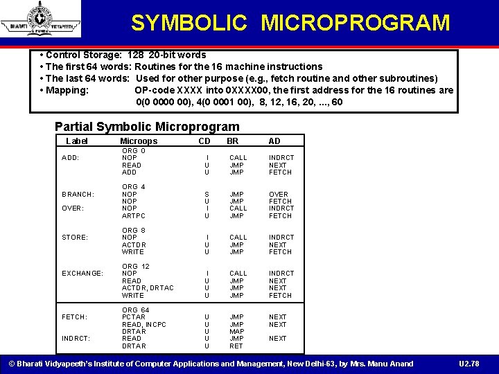
SYMBOLIC MICROPROGRAM • Control Storage: 128 20 -bit words • The first 64 words: Routines for the 16 machine instructions • The last 64 words: Used for other purpose (e. g. , fetch routine and other subroutines) • Mapping: OP-code XXXX into 0 XXXX 00, the first address for the 16 routines are 0(0 0000 00), 4(0 0001 00), 8, 12, 16, 20, . . . , 60 Partial Symbolic Microprogram Label ADD: BRANCH: OVER: STORE: EXCHANGE: FETCH: INDRCT: Microops BR AD I U U CALL JMP INDRCT NEXT FETCH ORG 4 NOP NOP ARTPC S U I U JMP CALL JMP OVER FETCH INDRCT FETCH ORG 8 NOP ACTDR WRITE I U U CALL JMP INDRCT NEXT FETCH ORG 12 NOP READ ACTDR, DRTAC WRITE I U U U CALL JMP JMP INDRCT NEXT FETCH ORG 64 PCTAR READ, INCPC DRTAR READ DRTAR U U U JMP MAP JMP RET NEXT ORG 0 NOP READ ADD CD NEXT © Bharati Vidyapeeth’s Institute of Computer Applications and Management, New Delhi-63, by Mrs. Manu Anand U 2. 78
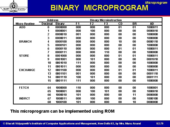
Microprogram BINARY MICROPROGRAM Micro Routine ADD BRANCH STORE EXCHANGE FETCH INDRCT Address Decimal Binary 0 0000000 1 0000001 2 0000010 3 0000011 4 0000100 5 0000101 6 0000110 7 0000111 8 0001000 9 0001001 10 0001010 11 0001011 12 0001100 13 0001101 14 0001110 15 0001111 64 65 66 67 68 1000000 1000001 1000010 1000011 1000100 F 1 000 000 000 111 000 001 100 111 Binary Microinstruction F 2 F 3 CD 000 01 100 000 000 000 10 000 000 01 000 110 00 000 01 101 000 000 000 01 000 00 101 000 000 00 BR 01 00 00 00 01 00 00 00 AD 1000011 0000010 1000000110 1000000 1000011 0001010 1000000 100001110 0001111 1000000 110 000 101 000 100 000 00 00 11 00 10 1000001 1000010 0000000 1000100 0000000 101 000 000 00 00 This microprogram can be implemented using ROM © Bharati Vidyapeeth’s Institute of Computer Applications and Management, New Delhi-63, by Mrs. Manu Anand U 2. 79
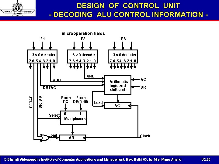
DESIGN OF CONTROL UNIT - DECODING ALU CONTROL INFORMATION microoperation fields F 1 F 2 F 3 3 x 8 decoder 7 6 54 3 21 0 76 54 3 21 0 AND ADD Arithmetic logic and shift unit DRTAR PCTAR DRTAC From PC DR(0 -10) Select Load AC DR AC 0 1 Multiplexers AR Clock © Bharati Vidyapeeth’s Institute of Computer Applications and Management, New Delhi-63, by Mrs. Manu Anand U 2. 80
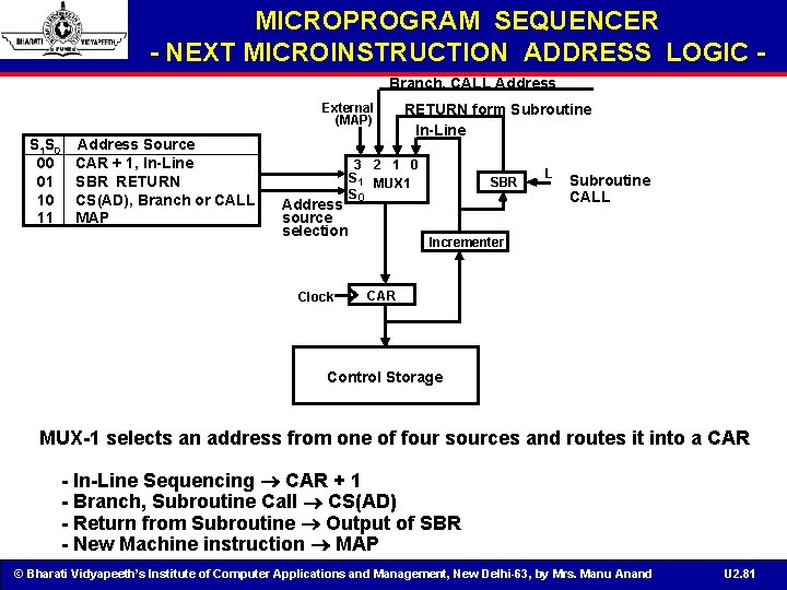
MICROPROGRAM SEQUENCER - NEXT MICROINSTRUCTION ADDRESS LOGIC Branch, CALL Address External (MAP) S 1 S 0 00 01 10 11 Address Source CAR + 1, In-Line SBR RETURN CS(AD), Branch or CALL MAP Address source selection Clock RETURN form Subroutine In-Line 3 2 1 0 S 1 MUX 1 S 0 SBR L Subroutine CALL Incrementer CAR Control Storage MUX-1 selects an address from one of four sources and routes it into a CAR - In-Line Sequencing CAR + 1 - Branch, Subroutine Call CS(AD) - Return from Subroutine Output of SBR - New Machine instruction MAP © Bharati Vidyapeeth’s Institute of Computer Applications and Management, New Delhi-63, by Mrs. Manu Anand U 2. 81
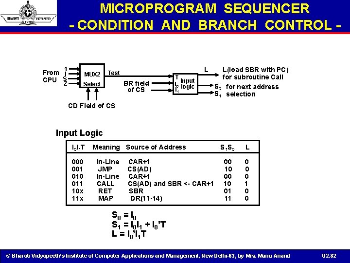
MICROPROGRAM SEQUENCER - CONDITION AND BRANCH CONTROL 1 From I CPU S MUX 2 Z L Test BR field of CS Select T Input I 0 logic I 1 L(load SBR with PC) for subroutine Call S 0 for next address S 1 selection CD Field of CS Input Logic I 0 I 1 T 000 001 010 011 10 x 11 x Meaning Source of Address In-Line JMP In-Line CALL RET MAP CAR+1 CS(AD) and SBR <- CAR+1 SBR DR(11 -14) S 1 S 0 L 00 10 01 11 0 0 0 1 0 0 S 0 = I 0 S 1 = I 0 I 1 + I 0’T L = I 0’I 1 T © Bharati Vidyapeeth’s Institute of Computer Applications and Management, New Delhi-63, by Mrs. Manu Anand U 2. 82
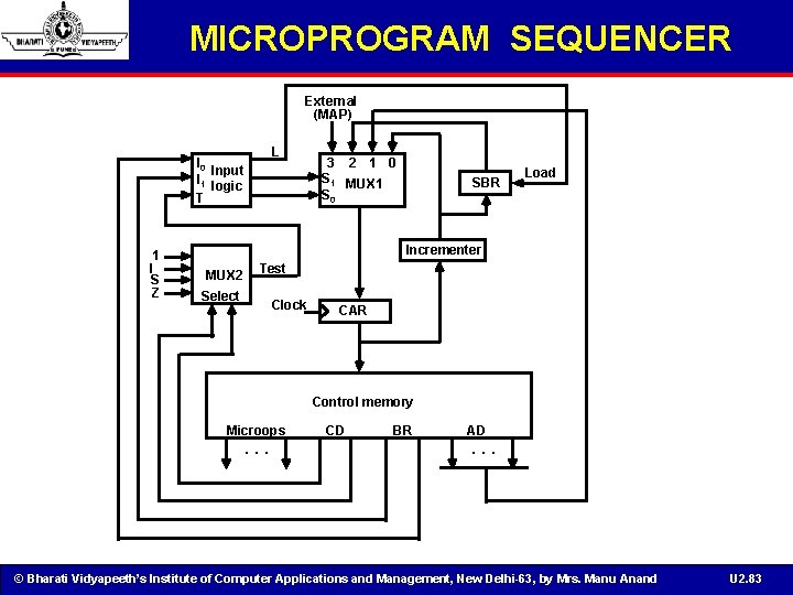
MICROPROGRAM SEQUENCER External (MAP) L I 0 Input I 1 logic T 1 I S Z 3 2 1 0 S 1 MUX 1 S 0 SBR Load Incrementer MUX 2 Test Select Clock CAR Control memory Microops . . . CD BR AD . . . © Bharati Vidyapeeth’s Institute of Computer Applications and Management, New Delhi-63, by Mrs. Manu Anand U 2. 83
MICROINSTRUCTION FORMAT Information in a Microinstruction - Control Information - Sequencing Information - Constant Information which is useful when feeding into the system These information needs to be organized in some way for - Efficient use of the microinstruction bits - Fast decoding Field Encoding - Encoding the microinstruction bits - Encoding slows down the execution speed due to the decoding delay - Encoding also reduces the flexibility due to the decoding hardware © Bharati Vidyapeeth’s Institute of Computer Applications and Management, New Delhi-63, by Mrs. Manu Anand U 2. 84
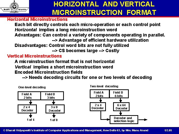
HORIZONTAL AND VERTICAL MICROINSTRUCTION FORMAT Horizontal Microinstructions Each bit directly controls each micro-operation or each control point Horizontal implies a long microinstruction word Advantages: Can control a variety of components operating in parallel. --> Advantage of efficient hardware utilization Disadvantages: Control word bits are not fully utilized --> CS becomes large --> Costly Vertical Microinstructions A microinstruction format that is not horizontal Vertical implies a short microinstruction word Encoded Microinstruction fields --> Needs decoding circuits for one or two levels of decoding Two-level decoding One-level decoding Field A 2 bits 2 x 4 Decoder 1 of 4 Field B 3 bits 3 x 8 Decoder 1 of 8 Field A 2 bits 2 x 4 Decoder Field B 6 bits 6 x 64 Decoder and selection logic © Bharati Vidyapeeth’s Institute of Computer Applications and Management, New Delhi-63, by Mrs. Manu Anand U 2. 85
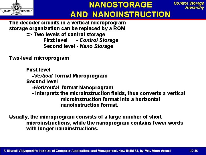
NANOSTORAGE AND NANOINSTRUCTION Control Storage Hierarchy The decoder circuits in a vertical microprogram storage organization can be replaced by a ROM => Two levels of control storage First level - Control Storage Second level - Nano Storage Two-level microprogram First level -Vertical format Microprogram Second level -Horizontal format Nanoprogram - Interprets the microinstruction fields, thus converts a vertical microinstruction format into a horizontal nanoinstruction format. Usually, the microprogram consists of a large number of short microinstructions, while the nanoprogram contains fewer words with longer nanoinstructions. © Bharati Vidyapeeth’s Institute of Computer Applications and Management, New Delhi-63, by Mrs. Manu Anand U 2. 86
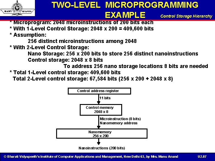
TWO-LEVEL MICROPROGRAMMING Control Storage Hierarchy EXAMPLE * Microprogram: 2048 microinstructions of 200 bits each * With 1 -Level Control Storage: 2048 x 200 = 409, 600 bits * Assumption: 256 distinct microinstructions among 2048 * With 2 -Level Control Storage: Nano Storage: 256 x 200 bits to store 256 distinct nanoinstructions Control storage: 2048 x 8 bits To address 256 nano storage locations 8 bits are needed * Total 1 -Level control storage: 409, 600 bits Total 2 -Level control storage: 67, 584 bits (256 x 200 + 2048 x 8) Control address register 11 bits Control memory 2048 x 8 Microinstruction (8 bits) Nanomemory address Nanomemory 256 x 200 Nanoinstructions (200 bits) © Bharati Vidyapeeth’s Institute of Computer Applications and Management, New Delhi-63, by Mrs. Manu Anand U 2. 87
CONCLUSIONS • • • Micro programmed control organization Address Sequencing Mapping of instruction Design of micro instructions Symbolic/Binary Micro program Design of control unit © Bharati Vidyapeeth’s Institute of Computer Applications and Management, New Delhi-63, by Mrs. Manu Anand U 2. 88
CENTRAL PROCESSING UNIT • Introduction • General Register Organization • Stack Organization • Instruction Formats • Addressing Modes • Data Transfer and Manipulation • Program Control • Reduced Instruction Set Computer © Bharati Vidyapeeth’s Institute of Computer Applications and Management, New Delhi-63, by Mrs. Manu Anand U 2. 89
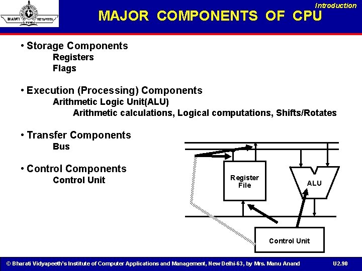
Introduction MAJOR COMPONENTS OF CPU • Storage Components Registers Flags • Execution (Processing) Components Arithmetic Logic Unit(ALU) Arithmetic calculations, Logical computations, Shifts/Rotates • Transfer Components Bus • Control Components Control Unit Register File ALU Control Unit © Bharati Vidyapeeth’s Institute of Computer Applications and Management, New Delhi-63, by Mrs. Manu Anand U 2. 90
REGISTERS • In Basic Computer, there is only one general purpose register, the Accumulator (AC) • In modern CPUs, there are many general purpose registers • It is advantageous to have many registers § Transfer between registers within the processor are relatively fast § Going “off the processor” to access memory is much slower • How many registers will be the best ? © Bharati Vidyapeeth’s Institute of Computer Applications and Management, New Delhi-63, by Mrs. Manu Anand U 2. 91
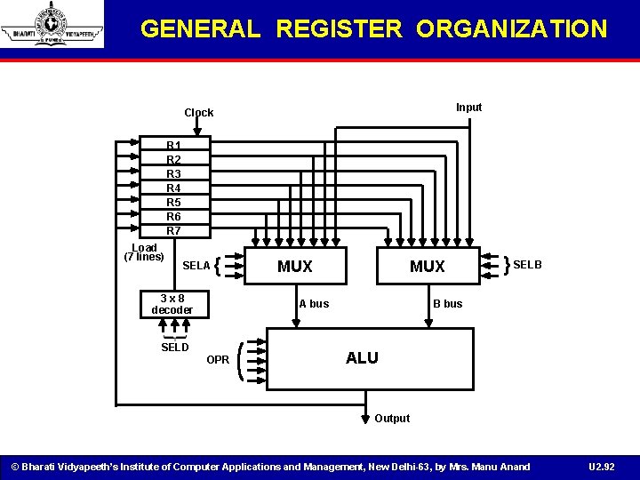
GENERAL REGISTER ORGANIZATION Input Clock R 1 R 2 R 3 R 4 R 5 R 6 R 7 Load (7 lines) SELA { 3 x 8 decoder MUX A bus SELD OPR } SELB B bus ALU Output © Bharati Vidyapeeth’s Institute of Computer Applications and Management, New Delhi-63, by Mrs. Manu Anand U 2. 92
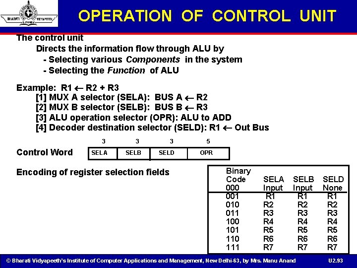
OPERATION OF CONTROL UNIT The control unit Directs the information flow through ALU by - Selecting various Components in the system - Selecting the Function of ALU Example: R 1 R 2 + R 3 [1] MUX A selector (SELA): BUS A R 2 [2] MUX B selector (SELB): BUS B R 3 [3] ALU operation selector (OPR): ALU to ADD [4] Decoder destination selector (SELD): R 1 Out Bus 3 Control Word SELA 3 SELB 3 SELD Encoding of register selection fields 5 OPR Binary Code 000 001 010 011 100 101 110 111 SELA Input R 1 R 2 R 3 R 4 R 5 R 6 R 7 SELB Input R 1 R 2 R 3 R 4 R 5 R 6 R 7 © Bharati Vidyapeeth’s Institute of Computer Applications and Management, New Delhi-63, by Mrs. Manu Anand SELD None R 1 R 2 R 3 R 4 R 5 R 6 R 7 U 2. 93
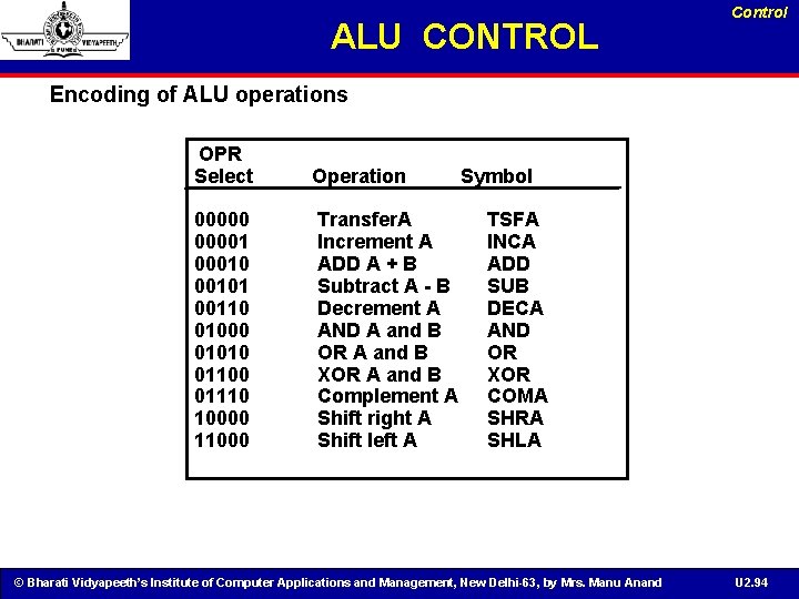
ALU CONTROL Control Encoding of ALU operations OPR Select Operation 000001 000101 00110 01000 01010 01100 01110 10000 11000 Transfer. A Increment A ADD A + B Subtract A - B Decrement A AND A and B OR A and B XOR A and B Complement A Shift right A Shift left A Symbol TSFA INCA ADD SUB DECA AND OR XOR COMA SHRA SHLA © Bharati Vidyapeeth’s Institute of Computer Applications and Management, New Delhi-63, by Mrs. Manu Anand U 2. 94
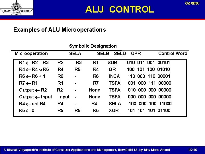
Control ALU CONTROL Examples of ALU Microoperations Symbolic Designation Microoperation SELA SELB SELD OPR Control Word R 1 R 2 R 3 R 4 R 5 R 6 + 1 R 7 R 1 R 2 R 4 R 6 R 1 R 3 R 5 - R 1 R 4 R 6 R 7 SUB OR INCA TSFA 010 011 00101 100 01010 110 00001 000 111 00000 Output R 2 Output Input R 4 shl R 4 R 5 0 R 2 Input R 4 R 5 None R 4 R 5 TSFA SHLA XOR 010 000 00000 100 11000 101 101 01100 © Bharati Vidyapeeth’s Institute of Computer Applications and Management, New Delhi-63, by Mrs. Manu Anand U 2. 95
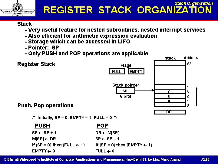
Stack Organization REGISTER STACK ORGANIZATION Stack - Very useful feature for nested subroutines, nested interrupt services - Also efficient for arithmetic expression evaluation - Storage which can be accessed in LIFO - Pointer: SP - Only PUSH and POP operations are applicable stack Register Stack 63 Flags FULL Address EMPTY Stack pointer SP 6 bits Push, Pop operations C B A 4 3 2 1 0 DR /* Initially, SP = 0, EMPTY = 1, FULL = 0 */ PUSH SP + 1 M[SP] DR If (SP = 0) then (FULL 1) EMPTY 0 POP DR M[SP] SP 1 If (SP = 0) then (EMPTY 1) FULL 0 © Bharati Vidyapeeth’s Institute of Computer Applications and Management, New Delhi-63, by Mrs. Manu Anand U 2. 96
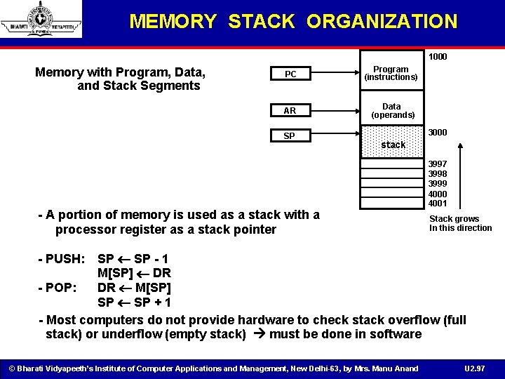
MEMORY STACK ORGANIZATION 1000 Memory with Program, Data, and Stack Segments PC Program (instructions) AR Data (operands) SP 3000 stack - A portion of memory is used as a stack with a processor register as a stack pointer 3997 3998 3999 4000 4001 Stack grows In this direction SP - 1 M[SP] DR - POP: DR M[SP] SP + 1 - Most computers do not provide hardware to check stack overflow (full stack) or underflow (empty stack) must be done in software - PUSH: © Bharati Vidyapeeth’s Institute of Computer Applications and Management, New Delhi-63, by Mrs. Manu Anand U 2. 97
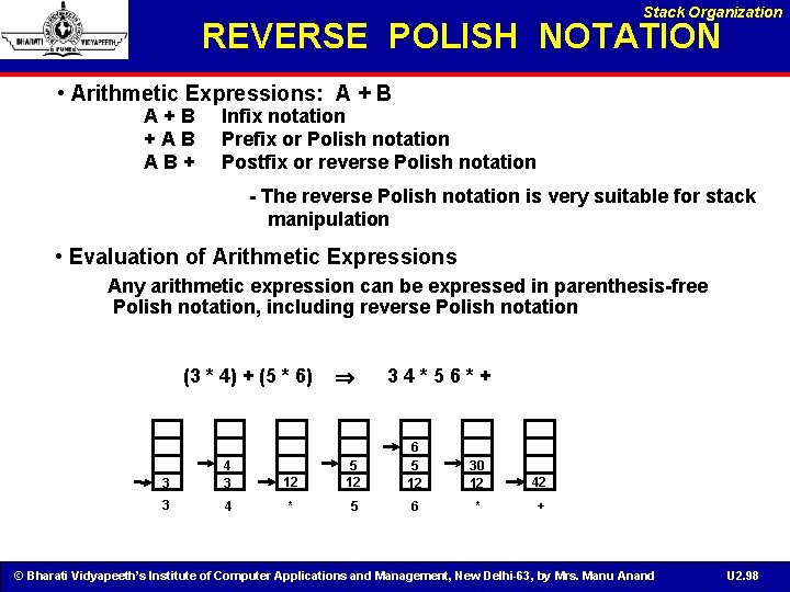
Stack Organization REVERSE POLISH NOTATION • Arithmetic Expressions: A + B A+B +AB AB+ Infix notation Prefix or Polish notation Postfix or reverse Polish notation - The reverse Polish notation is very suitable for stack manipulation • Evaluation of Arithmetic Expressions Any arithmetic expression can be expressed in parenthesis-free Polish notation, including reverse Polish notation (3 * 4) + (5 * 6) 3 4 3 12 5 12 3 4 * 5 34*56*+ 6 5 12 30 12 42 6 * + © Bharati Vidyapeeth’s Institute of Computer Applications and Management, New Delhi-63, by Mrs. Manu Anand U 2. 98
PROCESSOR ORGANIZATION • In general, most processors are organized in one of 3 ways • Single register (Accumulator) organization ü Basic Computer is a good example ü Accumulator is the only general purpose register • General register organization ü Used by most modern computer processors ü Any of the registers can be used as the source or destination for computer operations • Stack organization § All operations are done using the hardware stack § For example, an OR instruction will pop the two top elements from the stack, do a logical OR on them, and push the result on the stack © Bharati Vidyapeeth’s Institute of Computer Applications and Management, New Delhi-63, by Mrs. Manu Anand U 2. 99
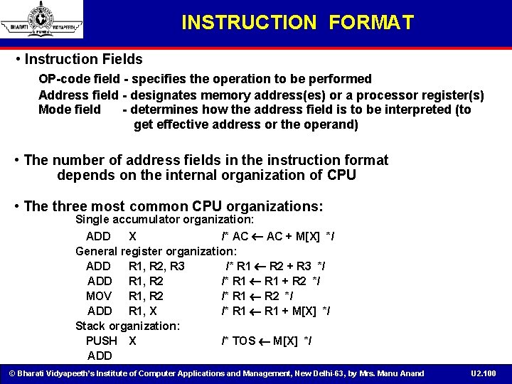
INSTRUCTION FORMAT • Instruction Fields OP-code field - specifies the operation to be performed Address field - designates memory address(es) or a processor register(s) Mode field - determines how the address field is to be interpreted (to get effective address or the operand) • The number of address fields in the instruction format depends on the internal organization of CPU • The three most common CPU organizations: Single accumulator organization: ADD X /* AC + M[X] */ General register organization: ADD R 1, R 2, R 3 /* R 1 R 2 + R 3 */ ADD R 1, R 2 /* R 1 + R 2 */ MOV R 1, R 2 /* R 1 R 2 */ ADD R 1, X /* R 1 + M[X] */ Stack organization: PUSH X /* TOS M[X] */ ADD © Bharati Vidyapeeth’s Institute of Computer Applications and Management, New Delhi-63, by Mrs. Manu Anand U 2. 100
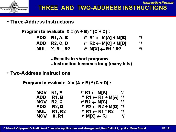
Instruction Format THREE AND TWO-ADDRESS INSTRUCTIONS • Three-Address Instructions Program to evaluate X = (A + B) * (C + D) : ADD R 1, A, B /* R 1 M[A] + M[B] ADD R 2, C, D /* R 2 M[C] + M[D] MUL X, R 1, R 2 /* M[X] R 1 * R 2 */ */ */ - Results in short programs - Instruction becomes long (many bits) • Two-Address Instructions Program to evaluate X = (A + B) * (C + D) : MOV ADD MUL MOV R 1, A R 1, B R 2, C R 2, D R 1, R 2 X, R 1 /* R 1 M[A] /* R 1 + M[A] /* R 2 M[C] /* R 2 + M[D] /* R 1 * R 2 /* M[X] R 1 */ */ */ © Bharati Vidyapeeth’s Institute of Computer Applications and Management, New Delhi-63, by Mrs. Manu Anand U 2. 101
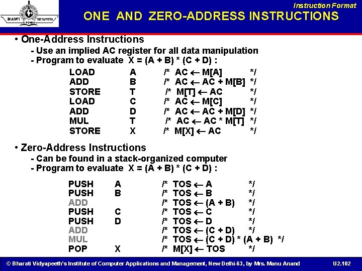
Instruction Format ONE AND ZERO-ADDRESS INSTRUCTIONS • One-Address Instructions - Use an implied AC register for all data manipulation - Program to evaluate X = (A + B) * (C + D) : LOAD A /* AC M[A] */ ADD B /* AC + M[B] */ STORE T /* M[T] AC */ LOAD C /* AC M[C] */ ADD D /* AC + M[D] */ MUL T /* AC * M[T] */ STORE X /* M[X] AC */ • Zero-Address Instructions - Can be found in a stack-organized computer - Program to evaluate X = (A + B) * (C + D) : PUSH ADD MUL POP A B C D X /* /* TOS A */ TOS B */ TOS (A + B) */ TOS C */ TOS D */ TOS (C + D) * (A + B) */ M[X] TOS */ © Bharati Vidyapeeth’s Institute of Computer Applications and Management, New Delhi-63, by Mrs. Manu Anand U 2. 102
ADDRESSING MODES • Addressing Modes * Specifies a rule for interpreting or modifying the address field of the instruction (before the operand is actually referenced) * Variety of addressing modes - to give programming flexibility to the user - to use the bits in the address field of the instruction efficiently © Bharati Vidyapeeth’s Institute of Computer Applications and Management, New Delhi-63, by Mrs. Manu Anand U 2. 103
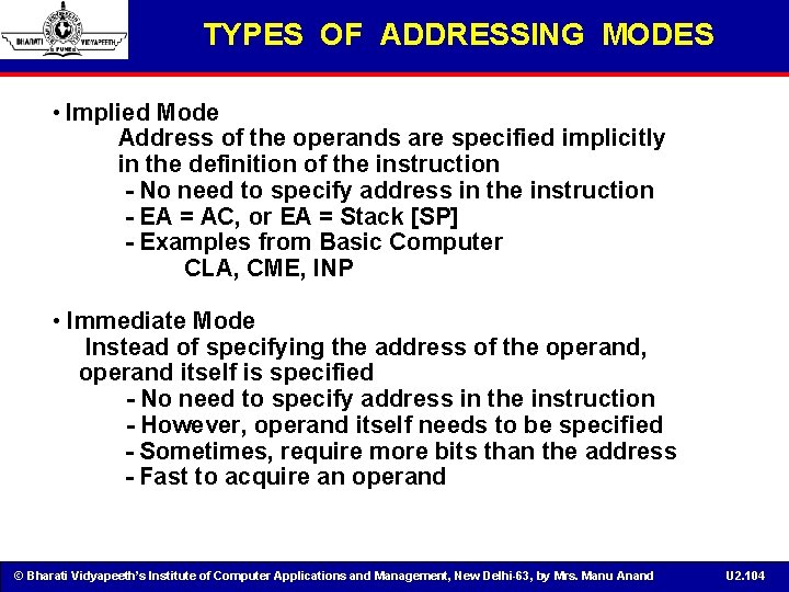
TYPES OF ADDRESSING MODES • Implied Mode Address of the operands are specified implicitly in the definition of the instruction - No need to specify address in the instruction - EA = AC, or EA = Stack [SP] - Examples from Basic Computer CLA, CME, INP • Immediate Mode Instead of specifying the address of the operand, operand itself is specified - No need to specify address in the instruction - However, operand itself needs to be specified - Sometimes, require more bits than the address - Fast to acquire an operand © Bharati Vidyapeeth’s Institute of Computer Applications and Management, New Delhi-63, by Mrs. Manu Anand U 2. 104
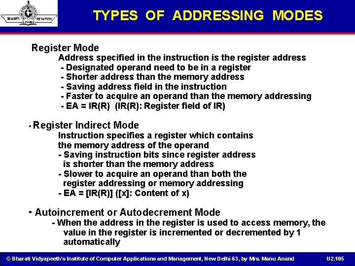
TYPES OF ADDRESSING MODES Register Mode Address specified in the instruction is the register address - Designated operand need to be in a register - Shorter address than the memory address - Saving address field in the instruction - Faster to acquire an operand than the memory addressing - EA = IR(R) (IR(R): Register field of IR) • Register Indirect Mode Instruction specifies a register which contains the memory address of the operand - Saving instruction bits since register address is shorter than the memory address - Slower to acquire an operand than both the register addressing or memory addressing - EA = [IR(R)] ([x]: Content of x) • Autoincrement or Autodecrement Mode - When the address in the register is used to access memory, the value in the register is incremented or decremented by 1 automatically © Bharati Vidyapeeth’s Institute of Computer Applications and Management, New Delhi-63, by Mrs. Manu Anand U 2. 105
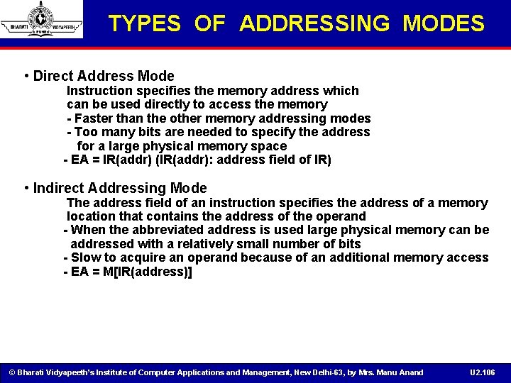
TYPES OF ADDRESSING MODES • Direct Address Mode Instruction specifies the memory address which can be used directly to access the memory - Faster than the other memory addressing modes - Too many bits are needed to specify the address for a large physical memory space - EA = IR(addr) (IR(addr): address field of IR) • Indirect Addressing Mode The address field of an instruction specifies the address of a memory location that contains the address of the operand - When the abbreviated address is used large physical memory can be addressed with a relatively small number of bits - Slow to acquire an operand because of an additional memory access - EA = M[IR(address)] © Bharati Vidyapeeth’s Institute of Computer Applications and Management, New Delhi-63, by Mrs. Manu Anand U 2. 106
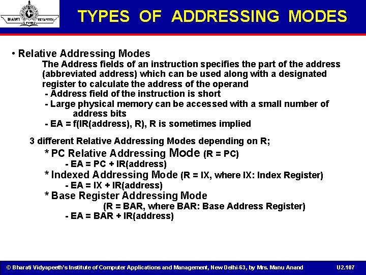
TYPES OF ADDRESSING MODES • Relative Addressing Modes The Address fields of an instruction specifies the part of the address (abbreviated address) which can be used along with a designated register to calculate the address of the operand - Address field of the instruction is short - Large physical memory can be accessed with a small number of address bits - EA = f(IR(address), R is sometimes implied 3 different Relative Addressing Modes depending on R; * PC Relative Addressing Mode (R = PC) - EA = PC + IR(address) * Indexed Addressing Mode (R = IX, where IX: Index Register) - EA = IX + IR(address) * Base Register Addressing Mode (R = BAR, where BAR: Base Address Register) - EA = BAR + IR(address) © Bharati Vidyapeeth’s Institute of Computer Applications and Management, New Delhi-63, by Mrs. Manu Anand U 2. 107
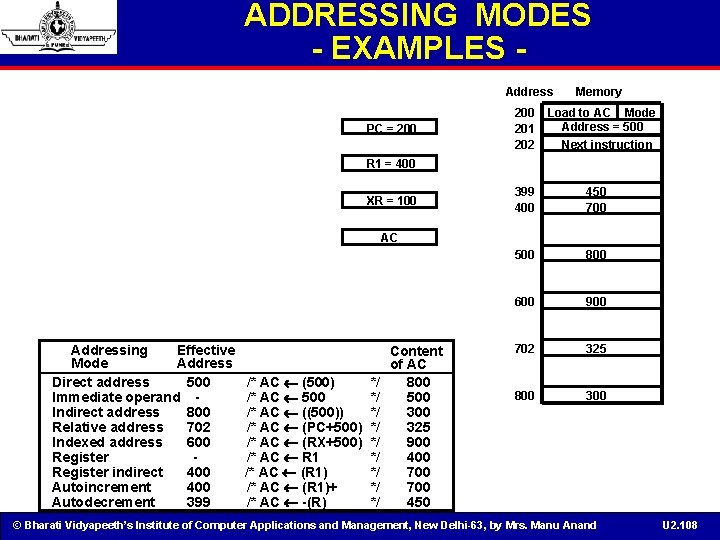
ADDRESSING MODES - EXAMPLES Address PC = 200 201 202 Memory Load to AC Mode Address = 500 Next instruction R 1 = 400 XR = 100 399 400 450 700 500 800 600 900 702 325 800 300 AC Addressing Effective Mode Address Direct address 500 Immediate operand Indirect address 800 Relative address 702 Indexed address 600 Register indirect 400 Autoincrement 400 Autodecrement 399 /* AC (500) /* AC 500 /* AC ((500)) /* AC (PC+500) /* AC (RX+500) /* AC R 1 /* AC (R 1)+ /* AC -(R) */ */ */ Content of AC 800 500 325 900 400 700 450 © Bharati Vidyapeeth’s Institute of Computer Applications and Management, New Delhi-63, by Mrs. Manu Anand U 2. 108
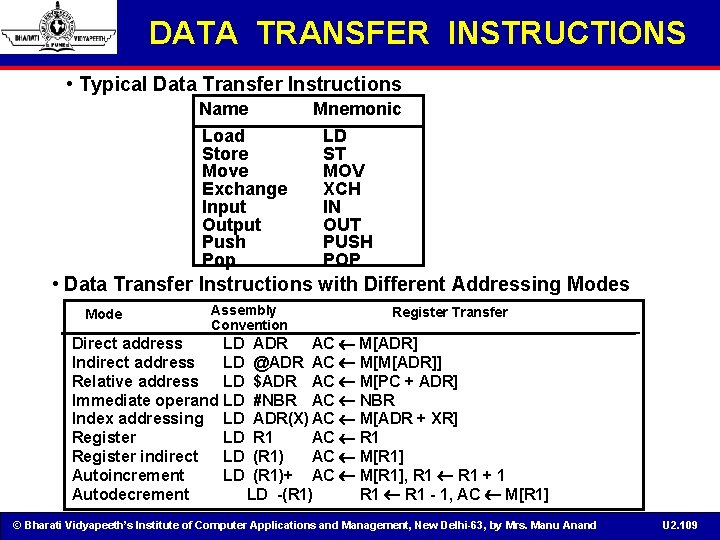
DATA TRANSFER INSTRUCTIONS • Typical Data Transfer Instructions Name Load Store Move Exchange Input Output Push Pop Mnemonic LD ST MOV XCH IN OUT PUSH POP • Data Transfer Instructions with Different Addressing Modes Mode Assembly Convention Register Transfer Direct address LD ADR AC M[ADR] Indirect address LD @ADR AC M[M[ADR]] Relative address LD $ADR AC M[PC + ADR] Immediate operand LD #NBR AC NBR Index addressing LD ADR(X) AC M[ADR + XR] Register LD R 1 AC R 1 Register indirect LD (R 1) AC M[R 1] Autoincrement LD (R 1)+ AC M[R 1], R 1 + 1 Autodecrement LD -(R 1) R 1 - 1, AC M[R 1] © Bharati Vidyapeeth’s Institute of Computer Applications and Management, New Delhi-63, by Mrs. Manu Anand U 2. 109
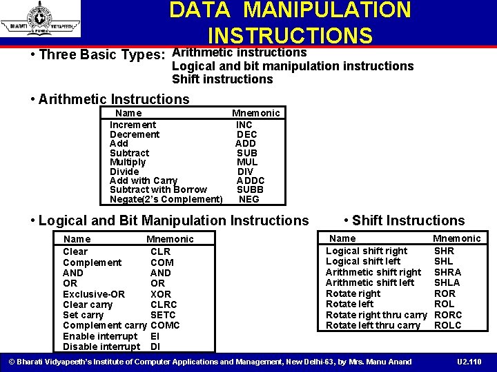
DATA MANIPULATION INSTRUCTIONS • Three Basic Types: Arithmetic instructions Logical and bit manipulation instructions Shift instructions • Arithmetic Instructions Name Mnemonic Increment INC Decrement DEC Add ADD Subtract SUB Multiply MUL Divide DIV Add with Carry ADDC Subtract with Borrow SUBB Negate(2’s Complement) NEG • Logical and Bit Manipulation Instructions Name Mnemonic Clear CLR Complement COM AND OR OR Exclusive-OR XOR Clear carry CLRC Set carry SETC Complement carry COMC Enable interrupt EI Disable interrupt DI • Shift Instructions Name Logical shift right Logical shift left Arithmetic shift right Arithmetic shift left Rotate right Rotate left Rotate right thru carry Rotate left thru carry © Bharati Vidyapeeth’s Institute of Computer Applications and Management, New Delhi-63, by Mrs. Manu Anand Mnemonic SHR SHL SHRA SHLA ROR ROL RORC ROLC U 2. 110
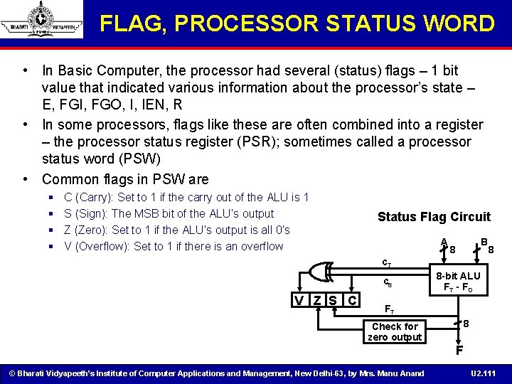
FLAG, PROCESSOR STATUS WORD • In Basic Computer, the processor had several (status) flags – 1 bit value that indicated various information about the processor’s state – E, FGI, FGO, I, IEN, R • In some processors, flags like these are often combined into a register – the processor status register (PSR); sometimes called a processor status word (PSW) • Common flags in PSW are § § C (Carry): Set to 1 if the carry out of the ALU is 1 S (Sign): The MSB bit of the ALU’s output Z (Zero): Set to 1 if the ALU’s output is all 0’s V (Overflow): Set to 1 if there is an overflow Status Flag Circuit A B 8 8 c 7 c 8 V Z S C 8 -bit ALU F 7 - F 0 F 7 8 Check for zero output F © Bharati Vidyapeeth’s Institute of Computer Applications and Management, New Delhi-63, by Mrs. Manu Anand U 2. 111
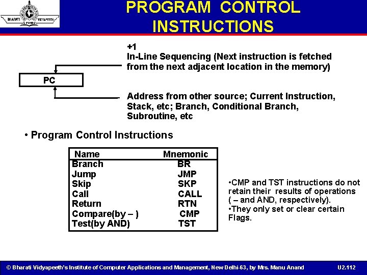
PROGRAM CONTROL INSTRUCTIONS +1 In-Line Sequencing (Next instruction is fetched from the next adjacent location in the memory) PC Address from other source; Current Instruction, Stack, etc; Branch, Conditional Branch, Subroutine, etc • Program Control Instructions Name Branch Jump Skip Call Return Compare(by ) Test(by AND) Mnemonic BR JMP SKP CALL RTN CMP TST • CMP and TST instructions do not retain their results of operations ( and AND, respectively). • They only set or clear certain Flags. © Bharati Vidyapeeth’s Institute of Computer Applications and Management, New Delhi-63, by Mrs. Manu Anand U 2. 112
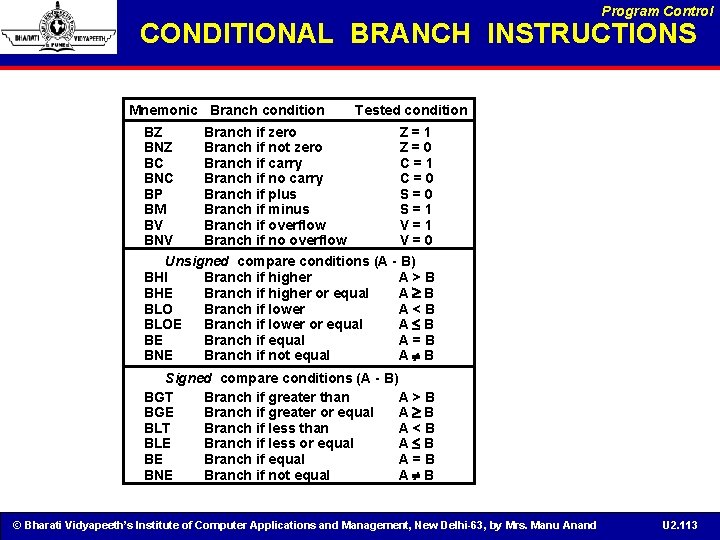
Program Control CONDITIONAL BRANCH INSTRUCTIONS Mnemonic Branch condition BZ BNZ BC BNC BP BM BV BNV Branch if zero Branch if not zero Branch if carry Branch if no carry Branch if plus Branch if minus Branch if overflow Branch if no overflow Tested condition Z=1 Z=0 C=1 C=0 S=1 V=0 Unsigned compare conditions (A - B) BHI Branch if higher A>B BHE Branch if higher or equal A B BLO Branch if lower A<B BLOE Branch if lower or equal A B BE Branch if equal A=B BNE Branch if not equal A B Signed compare conditions (A - B) BGT Branch if greater than A>B BGE Branch if greater or equal A B BLT Branch if less than A<B BLE Branch if less or equal A B BE Branch if equal A=B BNE Branch if not equal A B © Bharati Vidyapeeth’s Institute of Computer Applications and Management, New Delhi-63, by Mrs. Manu Anand U 2. 113
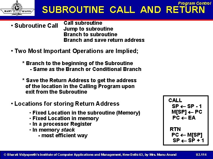
Program Control SUBROUTINE CALL AND RETURN Call subroutine • Subroutine Call Jump to subroutine Branch and save return address • Two Most Important Operations are Implied; * Branch to the beginning of the Subroutine - Same as the Branch or Conditional Branch * Save the Return Address to get the address of the location in the Calling Program upon exit from the Subroutine • Locations for storing Return Address • Fixed Location in the subroutine (Memory) • Fixed Location in memory • In a processor Register • In memory stack - most efficient way CALL SP - 1 M[SP] PC PC EA RTN PC M[SP] SP + 1 © Bharati Vidyapeeth’s Institute of Computer Applications and Management, New Delhi-63, by Mrs. Manu Anand U 2. 114
Program Control` PROGRAM INTERRUPT Types of Interrupts External interrupts External Interrupts initiated from the outside of CPU and Memory - I/O Device → Data transfer request or Data transfer complete - Timing Device → Timeout - Power Failure - Operator Internal interrupts (traps) Internal Interrupts are caused by the currently running program - Register, Stack Overflow - Divide by zero - OP-code Violation - Protection Violation Software Interrupts Both External and Internal Interrupts are initiated by the computer HW. Software Interrupts are initiated by the executing an instruction. - Supervisor Call → Switching from a user mode to the supervisor mode → Allows to execute a certain class of operations which are not allowed in the user mode © Bharati Vidyapeeth’s Institute of Computer Applications and Management, New Delhi-63, by Mrs. Manu Anand U 2. 115
Program Control INTERRUPT PROCEDURE Interrupt Procedure and Subroutine Call • The interrupt is usually initiated by an internal or an external signal rather than from the execution of an instruction (except for the software interrupt) • The address of the interrupt service program is determined by the hardware rather than from the address field of an instruction • An interrupt procedure usually stores all the information necessary to define the state of CPU rather than storing only the PC. • The state of the CPU is determined from; • Content of the PC • Content of all processor registers • Content of status bits • Many ways of saving the CPU state depending on the CPU architectures © Bharati Vidyapeeth’s Institute of Computer Applications and Management, New Delhi-63, by Mrs. Manu Anand U 2. 116
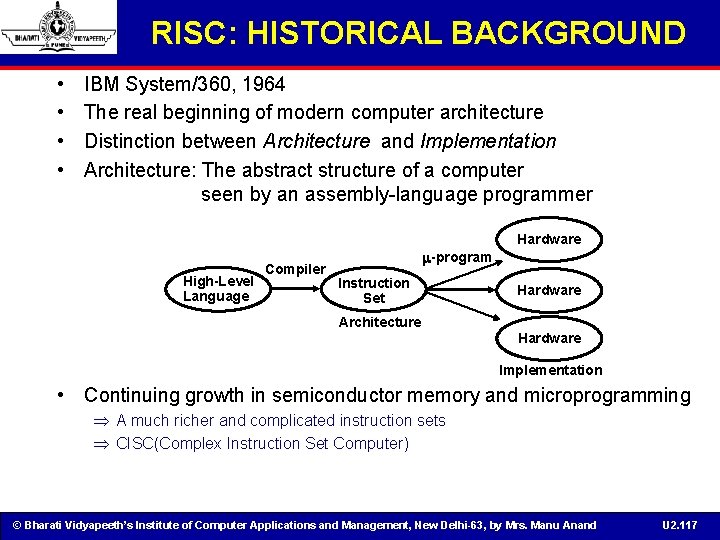
RISC: HISTORICAL BACKGROUND • • IBM System/360, 1964 The real beginning of modern computer architecture Distinction between Architecture and Implementation Architecture: The abstract structure of a computer seen by an assembly-language programmer Hardware High-Level Language Compiler -program Instruction Set Architecture Hardware Implementation • Continuing growth in semiconductor memory and microprogramming Þ A much richer and complicated instruction sets Þ CISC(Complex Instruction Set Computer) © Bharati Vidyapeeth’s Institute of Computer Applications and Management, New Delhi-63, by Mrs. Manu Anand U 2. 117
ARGUMENTS ADVANCED AT THAT TIME • Richer instruction sets would simplify compilers • Richer instruction sets would alleviate the software crisis § move as much functions to the hardware as possible • Richer instruction sets would improve architecture quality © Bharati Vidyapeeth’s Institute of Computer Applications and Management, New Delhi-63, by Mrs. Manu Anand U 2. 118
ARCHITECTURE DESIGN PRINCIPLES RISC - IN 70’s • Large microprograms would add little or nothing to the cost of the machine Rapid growth of memory technology Large General Purpose Instruction Set • Microprogram is much faster than the machine instructions Microprogram memory is much faster than main memory Moving the software functions into microprogram for the high performance machines • Execution speed is proportional to the program size Architectural techniques that led to small program High performance instruction set • Number of registers in CPU has limitations Very costly Difficult to utilize them efficiently © Bharati Vidyapeeth’s Institute of Computer Applications and Management, New Delhi-63, by Mrs. Manu Anand U 2. 119
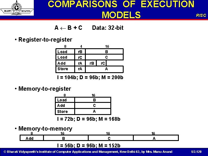
COMPARISONS OF EXECUTION RISC MODELS A B+C Data: 32 -bit • Register-to-register 8 Load Add Store 4 16 r. B r. C r. A B C r. C A r. B I = 104 b; D = 96 b; M = 200 b • Memory-to-register 8 Load Add Store 16 B C A I = 72 b; D = 96 b; M = 168 b • Memory-to-memory 8 16 16 16 Add B C A I = 56 b; D = 96 b; M = 152 b © Bharati Vidyapeeth’s Institute of Computer Applications and Management, New Delhi-63, by Mrs. Manu Anand U 2. 120
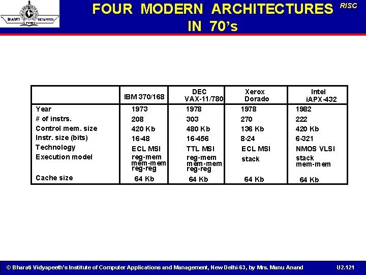
FOUR MODERN ARCHITECTURES IN 70’s IBM 370/168 Year # of instrs. Control mem. size Instr. size (bits) Technology Execution model Cache size 1973 208 420 Kb 16 -48 ECL MSI reg-mem mem-mem reg-reg 64 Kb DEC VAX-11/780 1978 303 480 Kb 16 -456 TTL MSI reg-mem mem-mem reg-reg 64 Kb Xerox Dorado 1978 270 136 Kb 8 -24 ECL MSI stack 64 Kb RISC Intel i. APX-432 1982 222 420 Kb 6 -321 NMOS VLSI stack mem-mem 64 Kb © Bharati Vidyapeeth’s Institute of Computer Applications and Management, New Delhi-63, by Mrs. Manu Anand U 2. 121
COMPLEX INSTRUCTION SET COMPUTER • These computers with many instructions and addressing modes came to be known as Complex Instruction Set Computers (CISC) • One goal for CISC machines was to have a machine language instruction to match each high -level language statement type © Bharati Vidyapeeth’s Institute of Computer Applications and Management, New Delhi-63, by Mrs. Manu Anand U 2. 122
VARIABLE LENGTH INSTRUCTIONS • The large number of instructions and addressing modes led CISC machines to have variable length instruction formats • The large number of instructions means a greater number of bits to specify them • In order to manage this large number of opcodes efficiently, they were encoded with different lengths: § More frequently used instructions were encoded using short opcodes. § Less frequently used ones were assigned longer opcodes. • Also, multiple operand instructions could specify different addressing modes for each operand § For example, ü Operand 1 could be a directly addressed register, ü Operand 2 could be an indirectly addressed memory location, ü Operand 3 (the destination) could be an indirectly addressed register. • All of this led to the need to have different length instructions in different situations, depending on the opcode and operands used © Bharati Vidyapeeth’s Institute of Computer Applications and Management, New Delhi-63, by Mrs. Manu Anand U 2. 123
Cont… • For example, an instruction that only specifies register operands may only be two bytes in length § One byte to specify the instruction and addressing mode § One byte to specify the source and destination registers. • An instruction that specifies memory addresses for operands may need five bytes § One byte to specify the instruction and addressing mode § Two bytes to specify each memory address ü Maybe more if there’s a large amount of memory. • Variable length instructions greatly complicate the fetch and decode problem for a processor • The circuitry to recognize the various instructions and to properly fetch the required number of bytes for operands is very complex © Bharati Vidyapeeth’s Institute of Computer Applications and Management, New Delhi-63, by Mrs. Manu Anand U 2. 124
COMPLEX INSTRUCTION SET COMPUTER • Another characteristic of CISC computers is that they have instructions that act directly on memory addresses § For example, ADD L 1, L 2, L 3 that takes the contents of M[L 1] adds it to the contents of M[L 2] and stores the result in location M[L 3] • An instruction like this takes three memory access cycles to execute • That makes for a potentially very long instruction execution cycle • The problems with CISC computers are § The complexity of the design may slow down the processor, § The complexity of the design may result in costly errors in the processor design and implementation, § Many of the instructions and addressing modes are used rarely, if ever © Bharati Vidyapeeth’s Institute of Computer Applications and Management, New Delhi-63, by Mrs. Manu Anand U 2. 125
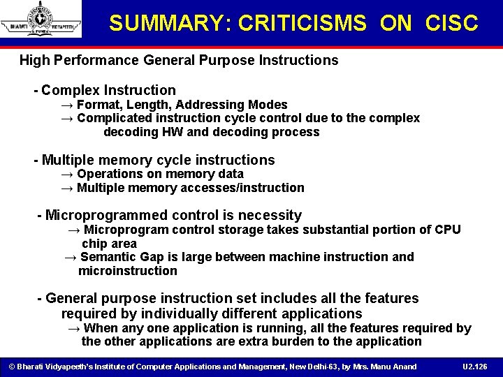
SUMMARY: CRITICISMS ON CISC High Performance General Purpose Instructions - Complex Instruction → Format, Length, Addressing Modes → Complicated instruction cycle control due to the complex decoding HW and decoding process - Multiple memory cycle instructions → Operations on memory data → Multiple memory accesses/instruction - Microprogrammed control is necessity → Microprogram control storage takes substantial portion of CPU chip area → Semantic Gap is large between machine instruction and microinstruction - General purpose instruction set includes all the features required by individually different applications → When any one application is running, all the features required by the other applications are extra burden to the application © Bharati Vidyapeeth’s Institute of Computer Applications and Management, New Delhi-63, by Mrs. Manu Anand U 2. 126
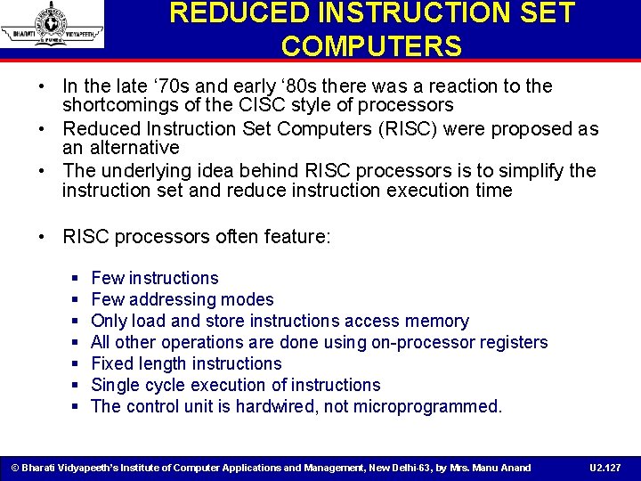
REDUCED INSTRUCTION SET COMPUTERS • In the late ‘ 70 s and early ‘ 80 s there was a reaction to the shortcomings of the CISC style of processors • Reduced Instruction Set Computers (RISC) were proposed as an alternative • The underlying idea behind RISC processors is to simplify the instruction set and reduce instruction execution time • RISC processors often feature: § § § § Few instructions Few addressing modes Only load and store instructions access memory All other operations are done using on-processor registers Fixed length instructions Single cycle execution of instructions The control unit is hardwired, not microprogrammed. © Bharati Vidyapeeth’s Institute of Computer Applications and Management, New Delhi-63, by Mrs. Manu Anand U 2. 127
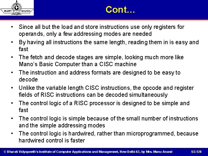
Cont… • Since all but the load and store instructions use only registers for operands, only a few addressing modes are needed • By having all instructions the same length, reading them in is easy and fast • The fetch and decode stages are simple, looking much more like Mano’s Basic Computer than a CISC machine • The instruction and address formats are designed to be easy to decode • Unlike the variable length CISC instructions, the opcode and register fields of RISC instructions can be decoded simultaneously • The control logic of a RISC processor is designed to be simple and fast • The control logic is simple because of the small number of instructions and the simple addressing modes • The control logic is hardwired, rather than microprogrammed, because hardwired control is faster © Bharati Vidyapeeth’s Institute of Computer Applications and Management, New Delhi-63, by Mrs. Manu Anand U 2. 128
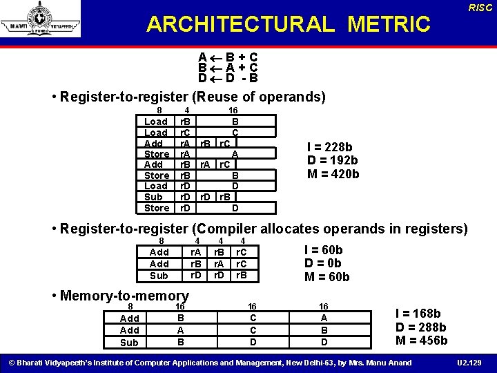
RISC ARCHITECTURAL METRIC A B+C B A+C D D -B • Register-to-register (Reuse of operands) 8 Load Add Store Load Sub Store 4 16 r. B B C r. A r. B r. C r. A A r. B r. A r. C r. B B r. D D r. B r. D D I = 228 b D = 192 b M = 420 b • Register-to-register (Compiler allocates operands in registers) 8 Add Sub • Memory-to-memory 4 4 4 r. A r. B r. D r. B r. A r. D r. C r. B I = 60 b D = 0 b M = 60 b 8 16 16 16 Add Sub B A B C C D A B D I = 168 b D = 288 b M = 456 b © Bharati Vidyapeeth’s Institute of Computer Applications and Management, New Delhi-63, by Mrs. Manu Anand U 2. 129
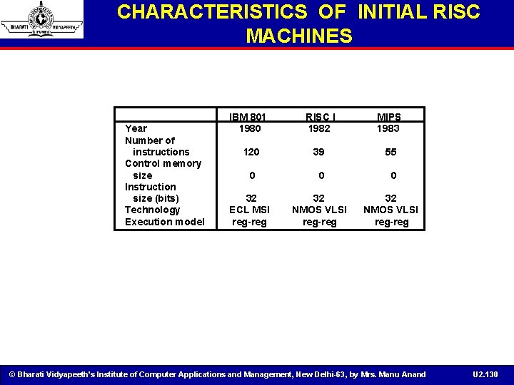
CHARACTERISTICS OF INITIAL RISC MACHINES Year Number of instructions Control memory size Instruction size (bits) Technology Execution model IBM 801 1980 RISC I 1982 MIPS 1983 120 39 55 0 0 0 32 NMOS VLSI reg-reg 32 ECL MSI reg-reg © Bharati Vidyapeeth’s Institute of Computer Applications and Management, New Delhi-63, by Mrs. Manu Anand U 2. 130
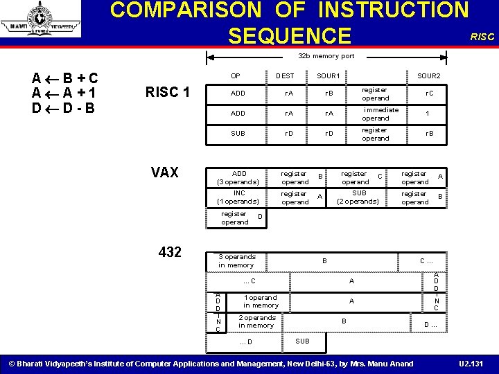
COMPARISON OF INSTRUCTION RISC SEQUENCE 32 b memory port A B+C A A+1 D D-B OP RISC 1 VAX DEST r. A r. B register operand r. C ADD r. A immediate operand 1 SUB r. D register operand r. B ADD (3 operands) register operand B INC (1 operands) register operand A register operand SUB (2 operands) register operand A register operand B B C. . . C A 1 operand in memory A 2 operands in memory. . . D C D 3 operands in memory A D D I N C SOUR 2 ADD register operand 432 SOUR 1 B A D D I N C D. . . SUB © Bharati Vidyapeeth’s Institute of Computer Applications and Management, New Delhi-63, by Mrs. Manu Anand U 2. 131
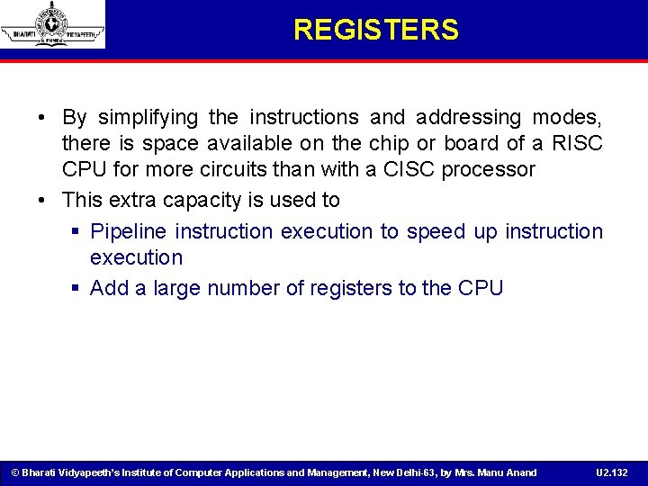
REGISTERS • By simplifying the instructions and addressing modes, there is space available on the chip or board of a RISC CPU for more circuits than with a CISC processor • This extra capacity is used to § Pipeline instruction execution to speed up instruction execution § Add a large number of registers to the CPU © Bharati Vidyapeeth’s Institute of Computer Applications and Management, New Delhi-63, by Mrs. Manu Anand U 2. 132
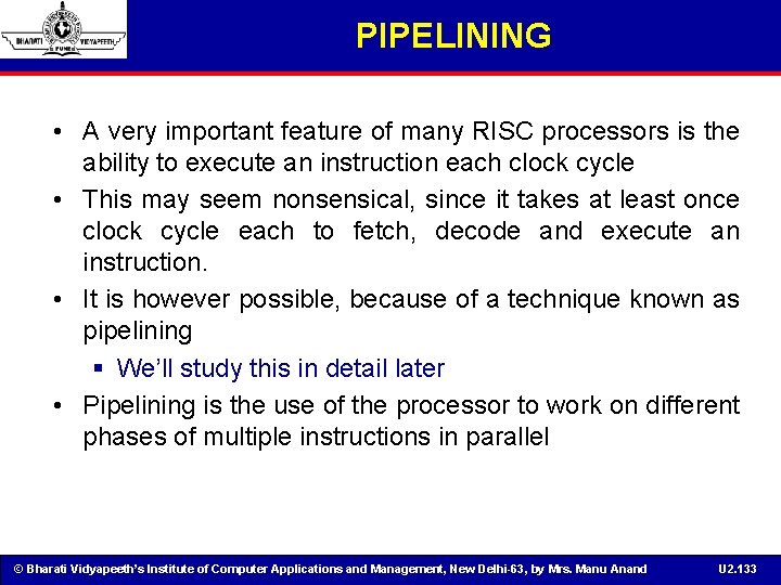
PIPELINING • A very important feature of many RISC processors is the ability to execute an instruction each clock cycle • This may seem nonsensical, since it takes at least once clock cycle each to fetch, decode and execute an instruction. • It is however possible, because of a technique known as pipelining § We’ll study this in detail later • Pipelining is the use of the processor to work on different phases of multiple instructions in parallel © Bharati Vidyapeeth’s Institute of Computer Applications and Management, New Delhi-63, by Mrs. Manu Anand U 2. 133
Cont… • For instance, at one time, a pipelined processor may be § Executing instruction it § Decoding instruction it+1 § Fetching instruction it+2 from memory • So, if we’re running three instructions at once, and it takes an average instruction three cycles to run, the CPU is executing an average of an instruction a clock cycle • As we’ll see when we cover it in depth, there are complications § For example, what happens to the pipeline when the processor branches • However, pipelined execution is an integral part of all modern processors, and plays an important role © Bharati Vidyapeeth’s Institute of Computer Applications and Management, New Delhi-63, by Mrs. Manu Anand U 2. 134
REGISTERS • By having a large number of general purpose registers, a processor can minimize the number of times it needs to access memory to load or store a value • This results in a significant speed up, since memory accesses are much slower than register accesses • Register accesses are fast, since they just use the bus on the CPU itself, and any transfer can be done in one clock cycle • To go off-processor to memory requires using the much slower memory (or system) bus • It may take many clock cycles to read or write to memory across the memory bus § The memory bus hardware is usually slower than the processor § There may even be competition for access to the memory bus by other devices in the computer (e. g. disk drives) • So, for this reason alone, a RISC processor may have an advantage over a comparable CISC processor, since it only needs to access memory § for its instructions, and § occasionally to load or store a memory value © Bharati Vidyapeeth’s Institute of Computer Applications and Management, New Delhi-63, by Mrs. Manu Anand U 2. 135
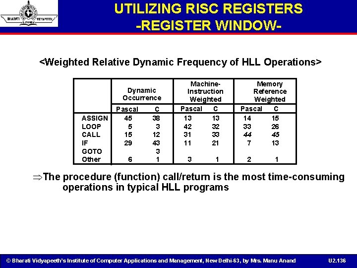
UTILIZING RISC REGISTERS -REGISTER WINDOW<Weighted Relative Dynamic Frequency of HLL Operations> Dynamic Occurrence ASSIGN LOOP CALL IF GOTO Other Pascal 45 5 15 29 6 C 38 3 12 43 3 1 Machine. Instruction Weighted Pascal C 13 13 42 32 31 33 11 21 3 1 Memory Reference Weighted Pascal C 14 15 33 26 44 45 7 13 2 1 ÞThe procedure (function) call/return is the most time-consuming operations in typical HLL programs © Bharati Vidyapeeth’s Institute of Computer Applications and Management, New Delhi-63, by Mrs. Manu Anand U 2. 136
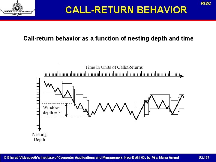
CALL-RETURN BEHAVIOR RISC Call-return behavior as a function of nesting depth and time © Bharati Vidyapeeth’s Institute of Computer Applications and Management, New Delhi-63, by Mrs. Manu Anand U 2. 137
RISC REGISTER WINDOW APPROACH • Observations • Weighted Dynamic Frequency of HLL Operations • Procedure call/return is the most time consuming operations • Locality of Procedure Nesting • The depth of procedure activation fluctuates within a relatively narrow range • A typical procedure employs only a few passed parameters and local variables • Solution • Use multiple small sets of registers (windows), each assigned to a different procedure • A procedure call automatically switches the CPU to use a different window of registers, rather than saving registers in memory • Windows for adjacent procedures are overlapped to allow parameter passing © Bharati Vidyapeeth’s Institute of Computer Applications and Management, New Delhi-63, by Mrs. Manu Anand U 2. 138
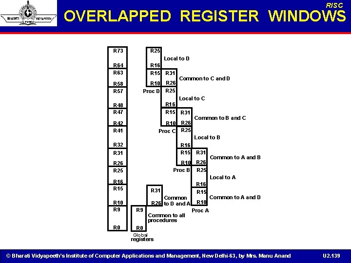
RISC OVERLAPPED REGISTER WINDOWS R 25 R 73 R 64 R 63 R 58 R 57 R 48 R 47 R 42 R 41 R 32 R 31 R 26 R 25 R 16 R 15 R 10 R 9 R 0 Local to D R 16 R 15 R 31 Common to C and D R 10 R 26 Proc D R 25 Local to C R 16 R 15 R 31 Common to B and C R 10 R 26 Proc C R 25 Local to B R 16 R 15 R 31 Common to A and B R 10 R 26 Proc B R 25 Local to A R 16 R 31 R 15 Common to A and D Common R 26 to D and A R 10 R 9 Proc A Common to all procedures R 0 Global registers © Bharati Vidyapeeth’s Institute of Computer Applications and Management, New Delhi-63, by Mrs. Manu Anand U 2. 139
OVERLAPPED REGISTER WINDOWS • There are three classes of registers: § Global Registers ü Available to all functions § Window local registers ü Variables local to the function § Window shared registers ü Permit data to be shared without actually needing to copy it • Only one register window is active at a time § The active register window is indicated by a pointer • When a function is called, a new register window is activated § This is done by incrementing the pointer • When a function calls a new function, the high numbered registers of the calling function window are shared with the called function as the low numbered registers in its register window • This way the caller’s high and the called function’s low registers overlap and can be used to pass parameters and results © Bharati Vidyapeeth’s Institute of Computer Applications and Management, New Delhi-63, by Mrs. Manu Anand U 2. 140
Cont… • In addition to the overlapped register windows, the processor has some number of registers, G, that are global registers § This is, all functions can access the global registers. • The advantage of overlapped register windows is that the processor does not have to push registers on a stack to save values and to pass parameters when there is a function call § Conversely, pop the stack on a function return • This saves § Accesses to memory to access the stack. § The cost of copying the register contents at all • And, since function calls and returns are so common, this results in a significant savings relative to a stack-based approach © Bharati Vidyapeeth’s Institute of Computer Applications and Management, New Delhi-63, by Mrs. Manu Anand U 2. 141
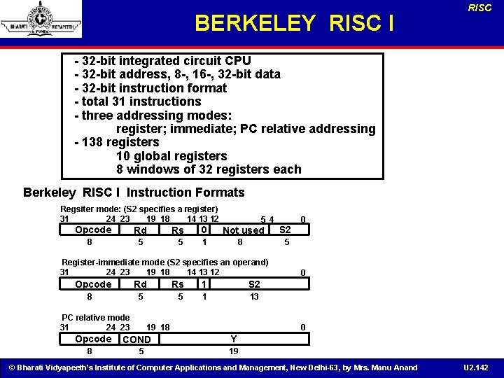
BERKELEY RISC I RISC - 32 -bit integrated circuit CPU - 32 -bit address, 8 -, 16 -, 32 -bit data - 32 -bit instruction format - total 31 instructions - three addressing modes: register; immediate; PC relative addressing - 138 registers 10 global registers 8 windows of 32 registers each Berkeley RISC I Instruction Formats Regsiter mode: (S 2 specifies a register) 31 24 23 19 18 14 13 12 Opcode Rd 8 5 Rs 0 5 1 5 4 Not used 8 5 Register-immediate mode (S 2 specifies an operand) 31 24 23 19 18 14 13 12 Opcode Rd 8 5 PC relative mode 31 24 23 Opcode 8 Rs 1 S 2 5 1 13 19 18 COND 5 S 2 0 0 0 Y 19 © Bharati Vidyapeeth’s Institute of Computer Applications and Management, New Delhi-63, by Mrs. Manu Anand U 2. 142
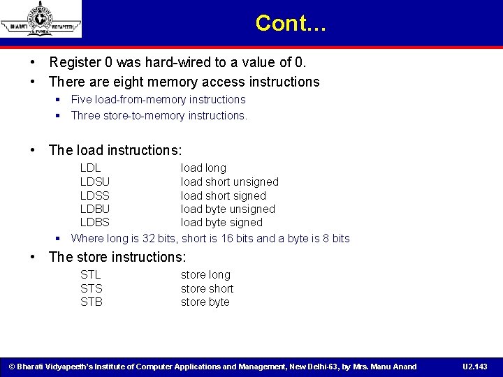
Cont… • Register 0 was hard-wired to a value of 0. • There are eight memory access instructions § Five load-from-memory instructions § Three store-to-memory instructions. • The load instructions: LDL load long LDSU load short unsigned LDSS load short signed LDBU load byte unsigned LDBS load byte signed § Where long is 32 bits, short is 16 bits and a byte is 8 bits • The store instructions: STL STS STB store long store short store byte © Bharati Vidyapeeth’s Institute of Computer Applications and Management, New Delhi-63, by Mrs. Manu Anand U 2. 143
![Cont… LDL Rd M[(Rs) + S 2] load long LDSU LDSS Rd M[(Rs) + Cont… LDL Rd M[(Rs) + S 2] load long LDSU LDSS Rd M[(Rs) +](http://slidetodoc.com/presentation_image/2aebcd7b1150f232858b7e02efb90c0c/image-144.jpg)
Cont… LDL Rd M[(Rs) + S 2] load long LDSU LDSS Rd M[(Rs) + S 2] load short unsigned load short signed LDBU LDBS Rd M[(Rs) + S 2] load byte unsigned load byte signed STL M[(Rs) + S 2] Rd store long STS M[(Rs) + S 2] Rd store short STB M[(Rs) + S 2] Rd store byte • Here the difference between the lengths is § A long is simply loaded, since it is the same size as the register (32 bits). § A short or a byte can be loaded into a register ü Unsigned - in which case the upper bits of the register are loaded with 0’s. ü Signed - in which case the upper bits of the register are loaded with the sign bit of the short/byte loaded. © Bharati Vidyapeeth’s Institute of Computer Applications and Management, New Delhi-63, by Mrs. Manu Anand U 2. 144
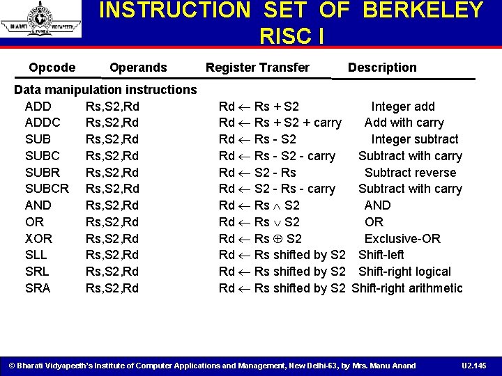
INSTRUCTION SET OF BERKELEY RISC I Opcode Operands Data manipulation instructions ADD Rs, S 2, Rd ADDC Rs, S 2, Rd SUBC Rs, S 2, Rd SUBR Rs, S 2, Rd SUBCR Rs, S 2, Rd AND Rs, S 2, Rd OR Rs, S 2, Rd XOR Rs, S 2, Rd SLL Rs, S 2, Rd SRA Rs, S 2, Rd Register Transfer Rd Rs + S 2 + carry Rd Rs - S 2 - carry Rd S 2 - Rs - carry Rd Rs S 2 Rd Rs shifted by S 2 Description Integer add Add with carry Integer subtract Subtract with carry Subtract reverse Subtract with carry AND OR Exclusive-OR Shift-left Shift-right logical Shift-right arithmetic © Bharati Vidyapeeth’s Institute of Computer Applications and Management, New Delhi-63, by Mrs. Manu Anand U 2. 145
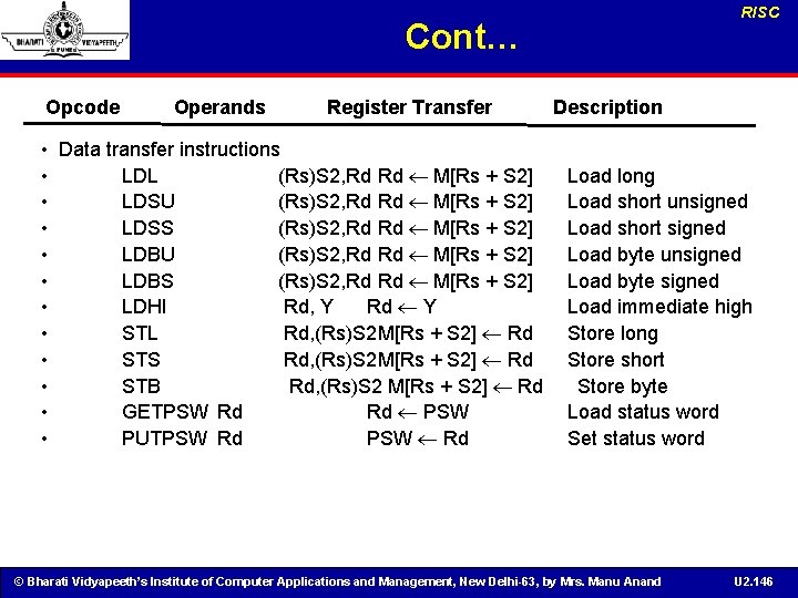
RISC Cont… Opcode Operands Register Transfer • Data transfer instructions • LDL (Rs)S 2, Rd Rd M[Rs + S 2] • LDSU (Rs)S 2, Rd Rd M[Rs + S 2] • LDSS (Rs)S 2, Rd Rd M[Rs + S 2] • LDBU (Rs)S 2, Rd Rd M[Rs + S 2] • LDBS (Rs)S 2, Rd Rd M[Rs + S 2] • LDHI Rd, Y Rd Y • STL Rd, (Rs)S 2 M[Rs + S 2] Rd • STS Rd, (Rs)S 2 M[Rs + S 2] Rd • STB Rd, (Rs)S 2 M[Rs + S 2] Rd • GETPSW Rd Rd PSW • PUTPSW Rd PSW Rd Description Load long Load short unsigned Load short signed Load byte unsigned Load byte signed Load immediate high Store long Store short Store byte Load status word Set status word © Bharati Vidyapeeth’s Institute of Computer Applications and Management, New Delhi-63, by Mrs. Manu Anand U 2. 146
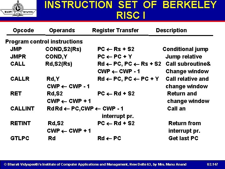
INSTRUCTION SET OF BERKELEY RISC I Opcode Operands Register Transfer Description Program control instructions JMP COND, S 2(Rs) JMPR COND, Y CALL Rd, S 2(Rs) CALLR RET CALLINT RETINT GTLPC PC Rs + S 2 Conditional jump PC + Y Jump relative Rd PC, PC Rs + S 2 Call subroutine& CWP - 1 Change window Rd, Y Rd PC, PC + Y Call relative and CWP - 1 change window Rd, S 2 PC Rd + S 2 Return and CWP + 1 change window Rd Rd PC, CWP - 1 Call an interrupt pr. Rd, S 2 PC Rd + S 2 Return from CWP + 1 interrupt pr. Rd Rd PC Get last PC © Bharati Vidyapeeth’s Institute of Computer Applications and Management, New Delhi-63, by Mrs. Manu Anand U 2. 147
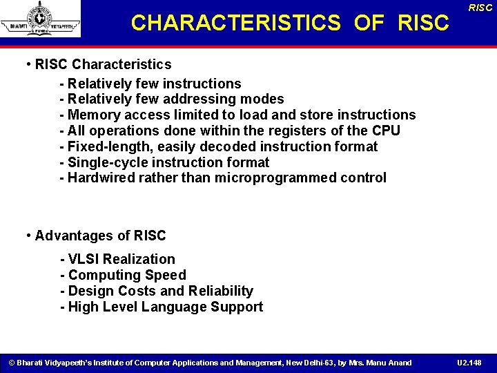
CHARACTERISTICS OF RISC • RISC Characteristics - Relatively few instructions - Relatively few addressing modes - Memory access limited to load and store instructions - All operations done within the registers of the CPU - Fixed-length, easily decoded instruction format - Single-cycle instruction format - Hardwired rather than microprogrammed control • Advantages of RISC - VLSI Realization - Computing Speed - Design Costs and Reliability - High Level Language Support © Bharati Vidyapeeth’s Institute of Computer Applications and Management, New Delhi-63, by Mrs. Manu Anand U 2. 148
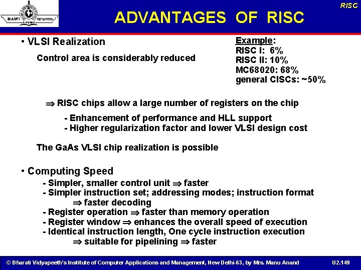
ADVANTAGES OF RISC • VLSI Realization Control area is considerably reduced RISC Example: RISC I: 6% RISC II: 10% MC 68020: 68% general CISCs: ~50% RISC chips allow a large number of registers on the chip - Enhancement of performance and HLL support - Higher regularization factor and lower VLSI design cost The Ga. As VLSI chip realization is possible • Computing Speed - Simpler, smaller control unit faster - Simpler instruction set; addressing modes; instruction format faster decoding - Register operation faster than memory operation - Register window enhances the overall speed of execution - Identical instruction length, One cycle instruction execution suitable for pipelining faster © Bharati Vidyapeeth’s Institute of Computer Applications and Management, New Delhi-63, by Mrs. Manu Anand U 2. 149
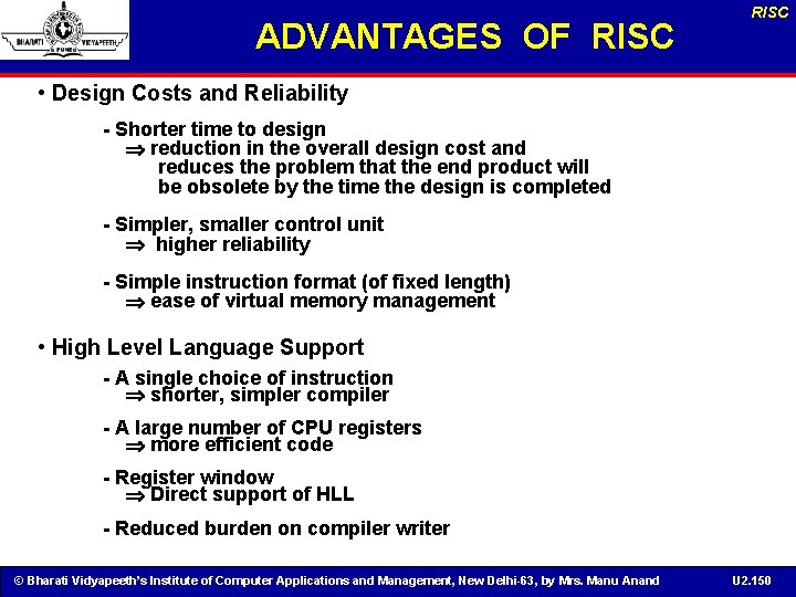
ADVANTAGES OF RISC • Design Costs and Reliability - Shorter time to design reduction in the overall design cost and reduces the problem that the end product will be obsolete by the time the design is completed - Simpler, smaller control unit higher reliability - Simple instruction format (of fixed length) ease of virtual memory management • High Level Language Support - A single choice of instruction shorter, simpler compiler - A large number of CPU registers more efficient code - Register window Direct support of HLL - Reduced burden on compiler writer © Bharati Vidyapeeth’s Institute of Computer Applications and Management, New Delhi-63, by Mrs. Manu Anand U 2. 150
CONCLUSIONS • • • CPU Organizations Addressing Modes Address Instructions Classification of computer instructions RISC/CISC © Bharati Vidyapeeth’s Institute of Computer Applications and Management, New Delhi-63, by Mrs. Manu Anand U 2. 151
OBJECTIVE QUESTIONS 1. 2. 3. 4. 5. 6. A CPU’s microinstruction format has five separate control fields. The number of micro operations in each fields are as follows F 1=4, F 2 = 4, F 3 = 3, F 4 = 12, F 5 = 21 i. What is the total length of microinstrcution needed to accommodate the five control fields ii. If pure horizontal microprogramming is followed without encoding, what will be the length of microinstruction? Pick out the incorrect RTL statement and indicate the problems 1. PC: = MAR, PC: = PC+1 2. MR: =1, Pc: =PC+1 NOOP instruction requires nothing (no action) to be performed for the instruction. This is true for macro operation level but false for the microoperation level. The control unit must perform one microoperation which is necessary for any instruction. Identify the essential micro operation which is performed for NOOP instruction. Is nano and micro programming same? The address of stack is stored in _______ In __________addressing mode the content of PC is added to address part of the instruction in order to obtain the effective address © Bharati Vidyapeeth’s Institute of Computer Applications and Management, New Delhi-63, by Mrs. Manu Anand U 2. 152
Cont… 7. Control word specifies ________ 8. Memory unit that stores the control word is ______ 9. ____ is program which convert symbolic language into machine code. 10. ____ is also called nexr address generator. 11. The instructions which copy information from one location to another either in the processor’s internal register set or in the external main memory are called a. Data transfer instructions. b. Program control instructions. c. Input-output instructions. d. Logical instructions. 12. If the value V(x) of the target operand is contained in the address field itself, the addressing mode is a. immediate. b. direct. c. indirect. d. implied. 13. A microprogram sequencer a. generates the address of next micro instruction to be executed. b. generates the control signals to execute a microinstruction. c sequentially averages all microinstructions in the control memory. d. enables the efficient handling of a micro program subroutine. © Bharati Vidyapeeth’s Institute of Computer Applications and Management, New Delhi-63, by Mrs. Manu Anand U 2. 153
Cont… 14. During what CPU cycle is an instruction moved from primary storage to the control unit? a. fetch b. execution c. access d. refresh 15. What type of processor does not directly implement instructions that combine data movement and manipulation? a. CISC b. RISC c. microprocessor d. PSW 16. When the control unit fetches an instruction from memory, it stores it in the ____. a. instruction pointer b. program status word c. op code d. instruction register © Bharati Vidyapeeth’s Institute of Computer Applications and Management, New Delhi-63, by Mrs. Manu Anand U 2. 154
Cont… 17. Which of the following is a storage location that holds inputs and outputs for the ALU? a. Control unit b. ALU c. I/O device d. Register 18. The ____ tests the bit values in the source location and places copies of those values in the destination location. a. LOAD b. MOVE c. STORE d. ADD © Bharati Vidyapeeth’s Institute of Computer Applications and Management, New Delhi-63, by Mrs. Manu Anand U 2. 155
SHORT QUESTIONS 1. 2. 3. 4. 5. 6. 7. The instruction length and operand address field is 36 bits and 14 bits respectively. If two – operand instructions of 240 numbers are used, then how many one operand instructions are possible? The stack based CPU don’t have registers for storing the operands. Can we conclude that the stack based CPU has less hardware circuit and cheaper than register based CPU? The instruction format of a CPU is designed for the two types (a) op-code and three fields for register address; (b) op-code and one field for memory address. Identify different formats for instructions. Difference between horizontal and vertical instruction format. What is firmware? How it is different from software and hardware? A register based CPU can be viewed as multiple accumulators based CPU. Justify this statement A micro programmed CPU has 1 K words in the control memory. Each instruction needs 8 microinstructions. Assuming that the op-code in the macro instruction is of 5 bits length, propose a mapping scheme to generate control memory address for the op-code. © Bharati Vidyapeeth’s Institute of Computer Applications and Management, New Delhi-63, by Mrs. Manu Anand U 2. 156
Cont… 8. Name some functions of control unit. 9. What is the difference between internal and software interrupts? 10. A computer has 32 bit instructions and 12 bit addresses. If there are 250 two address instruction, how many one address instruction can be formulated? 11. What is the Fetch routine in Micro programmed control unit 12. The instructions are classified on the basis of following factors 1. Op-code: _______ 2. Data: _________, etc 3. Operand location: _____, _______ 4. Operand addressing: ___________ 5. Instruction length: _______, _____ 6. No. of address field______, _______ © Bharati Vidyapeeth’s Institute of Computer Applications and Management, New Delhi-63, by Mrs. Manu Anand U 2. 157
LONG QUESTIONS 1. 2. 3. 4. 5. Write an assembly language program to derive the expression X=(A+B)(C+D) for an accumulator, register and stack based CPU What is addressing mode? Discuss different types of addressing modes with its advantages and disadvantages. A program has three jump instructions in three consecutive words (locations) in memory: 0111, 1000 and 1001. The corresponding jump addresses are 1001, 0111 respectively. Suppose we load 0111. Initially in PC and start the CPU, how many times will the instruction in location be fetched and executed? A 32 -bit CPU has 16 -bit instruction and 12 -bit memory address. Its memory is organized as 4 K of 32 -bits each. Each memory word stores two instructions. The instruction format has 4 -bits for op-code. The CPU’s instruction register can accommodate two instructions. Suggest a design strategy for the instruction cycle sequence. What is the basic difference between a branch instruction, a call subroutine instruction, and a program interrupt? Explain various types of interrupts and give examples of each. © Bharati Vidyapeeth’s Institute of Computer Applications and Management, New Delhi-63, by Mrs. Manu Anand U 2. 158
Cont. . 6. A processor has following hardware configuration a. No. of registers=8 b. ALU operations: arithmetic 8, logic 8 c. Shifter : 4 operations d. Bus: single bus Design the microinstruction format for this CPU 7. A digital computer has a common bus system for 12 registers of 9 bits each. The bus is constructed with multiplexers. a. How many selection inputs are there in each multiplexer? b. What size of multiplexers are needed? c. How many multiplexers are there in the bus? d. Draw a diagram of the bus system using three-state buffers and a decoder instead of multiplexers? 8. The system uses a control memory of 1024 words of 32 bits each. The microinstruction has three fields for micro-operations. select a status bit and Brach address field. The micro-operation field has 16 bits. a. How many bits are there in the branch address field and select field? b. If there are 16 status bits in the system, how many bits of the branch logic are used to select a status bit? c. How many bits are left to select the input to the multiplexers? © Bharati Vidyapeeth’s Institute of Computer Applications and Management, New Delhi-63, by Mrs. Manu Anand U 2. 159
Cont. . 9. Write micro operation for BSA and ISZ 10. A computer has following registers PC(12 bits), MAR(16), MBR(12), I(1), OPR(3), E(1), AC(16) and six timing signal t 0 to t 5 and one flip-flop F for cycle control. Fetch cycle is performed when F=0 and execute cycle when F=1. List the micro-operations and control functions for the computer (i) When F=0 (ii) For Executing XOR, SWAP (AC and memory Word) ADD (M M+AC) 11. A digital system has 16 registers, each with 32 -bits. It is necessary to provide parallel data transfer from each register to every other register a. How many lines are needed for direct parallel transfer? b. If we need to link these register to a common bus c. How many Multiplexer will be required? d. How many input lines are required for each multiplexer 12. In a seven register bus organization of CPU the propagation delays are given, 30 s for multiplexer, 60 ns to perform the add operation in the ALU and 20 ns in the destination decoder, and 10 ns to clock the data into destination register. What is the minimum cycle time that can be used for the clock © Bharati Vidyapeeth’s Institute of Computer Applications and Management, New Delhi-63, by Mrs. Manu Anand U 2. 160
RESEARCH PROBLEM 1. What are the differences between CISC and RISC architectures? Which types of applications are properly suited for each of these categories of architecture? Compare and contrast CISC architecture and RISC architecture. Make sure to include the strengths and weaknesses of each as well as applications to which they would be most suited. You may also compare/contrast them with any architecture that may be considered as future replacements for either or both of these two. © Bharati Vidyapeeth’s Institute of Computer Applications and Management, New Delhi-63, by Mrs. Manu Anand U 2. 161
REFERENCES 1. 2. 3. 4. 5. 6. Hayes P. John, Computer Architecture and Organisation, Mc. Graw Hill Comp. , 1988. Mano M. , Computer System Architecture, Prentice-Hall Inc. 1993. Patterson, D. , Hennessy, J. , Computer Architecture - A Quantitative Approach, second edition, Morgan Kaufmann Publishers, Inc. 1996; Stallings, William, Computer Organization and Architecture, 5 th edition, Prentice Hall International, Inc. , 2000. Tanenbaum, A. , Structured Computer Organization, 4 th ed. , Prentice- Hall Inc. 1999. Hamacher, Vranesic, Zaky, Computer Organization, 4 th ed. , Mc. Graw Hill Comp. , 1996. © Bharati Vidyapeeth’s Institute of Computer Applications and Management, New Delhi-63, by Mrs. Manu Anand U 2. 162
- Slides: 162