UNITI 80386 DX functional Block Diagram PIN Description

UNIT-I • 80386 DX functional Block Diagram • PIN Description • Register set • Flags • Physical address space • Data types

80386 DX Feature �It supports 8/16/32 bit data operands �It has 32 -bit internal registers �It supports 32 -bit data bus and 32 -bit non-multiplexed address bus �It supports � Physical Address of 4 GB � Virtual Address of 64 TB � Maximum Segment size of 4 GB �It operates in 3 different modes � Real � Protected � Virtual 8086 �MMU provides virtual memory, paging and 4 levels of protection �Clock Frequency : 20, 25 and 33 MHz �It has 132 pin package

80386 DX functional Block Diagram
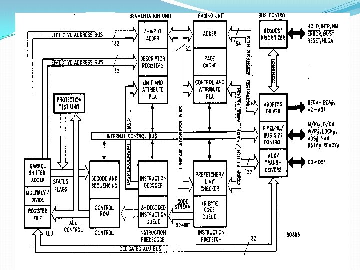

Internal Architecture 80386 is divided into three sections: �Central Processing Unit �Memory Management Unit �Bus Interface unit

Central Processing Unit The CPU divided into � Instruction Unit: �It decodes the opcode bytes received from the 16 -byte instruction queue and arranges them into a 3 -decoded instruction queue. �After decoding it is passed to control section for deriving necessary control signals �Execution Unit: �It has 8 general purpose and 8 special purpose registers which either handles data or addresses �The 64 -bit barrel shifter increases the speed of all shift, rotate, multiply and divide operations �The multiply/divide logic implements the bit-shift-rotate algorithms to complete the operations in minimum time(Even 32 bit multiplication is done in 1µs)
: Performs the operation identified by ADD, SUB,")
Elements of Execution Unit �Arithmetic/logic unit (ALU): Performs the operation identified by ADD, SUB, AND, etc. �Flags register: Holds status and control information �General-purpose registers: Holds address or data information �Control ROM: Contains microcode sequences that define operations performed by machine instructions �Special multiply, shift, and barrel shift hardware: Accelerate multiply, divide, and rotate operations

Memory Management Unit �It consists of a segmentation unit and paging unit �Segmentation Unit: �It allows the use of two address components - segment and offset – for relocability and sharing of data �It allows a maximum segment size of 4 GB �It provides a 4 -level protection mechanism for protecting and isolating system’s code and data from those of application program �The limit and attribute PLA checks segment limits and attributes at segment level to avoid invalid accesses to code and data in memory segment.

Memory Management Unit �Paging Unit �It organizes physical memory in terms of pages of 4 KB size �It works under the control of segmentation unit �It converts linear addresses into physical addresses �The control and attribute PLA checks privileges at page level.

Bus Interface Unit �It has a prioritizer to resolve the priority of various bus requests. This controls the access of the bus �The address driver drives the bus enable and address signals A 2 – A 31. �The pipeline/bus size unit handles the control signals for pipelining and dynamic bus sizing units �The data buffers interface the internal data bus with system bus

PIN Description

PIN Description �# symbol indicates active low signal. �When no # is present, the signal is active high. Example: M/IO# � - High voltage indicates memory selected �- Low voltage indicates I/O selected
: It is divided by two internally to generate the")
PIN Description �Clock (CLK 2): It is divided by two internally to generate the internal processor clock. � Data Bus (D 0 through D 31): �It has three-state bidirectional signals. �It can transfer data on 32 - and 16 -bit buses using a data bus sizing feature. �Address Bus (A 2 through A 31) �These three-state outputs provide memory or I/O port addresses. �It can access 4 GB of physical memory from 0000 H to FFFFH �Of the total 32 -bits, only higher 30 are released by MP �A 1 & A 0 are used internally by MP to produce 4 bank enable signals(BE 3# - BE 0#)
 �enable 4 memory banks")
PIN Description �Byte Enable Outputs( BE 0# -- BE 3#) �enable 4 memory banks �indicates which bytes of the 32 -bit data bus are involved with the current transfer. �BE 0# applies to D 0 -D 7 �BE 1# applies to D 8 -D 15 �BE 2# applies to D 16 -D 23 �BE 3# applies to D 24 -D 31 �No. of Byte Enables asserted indicates physical size of operand being transferred (1, 2, 3, or 4 bytes).

PIN Description

PIN Description BE 3# 1 1 0 1 BE 2# 1 1 1 0 0 0 BE 1# 1 1 0 0 1 0 BE 0# 1 0 1 1 0 Operation No Operation Bank 0 (8 -bit) Bank 1 (8 -bit) Bank 2 (8 -bit) Bank 3 (8 -bit) Bank 0, 1 (16 -bit) Bank 1, 2 (16 -bit) Bank 2, 3 (16 -bit) Bank 0, 1, 2(24 -bit) 0 0 0 1 Bank 1, 2, 3(24 -bit) 0 0 Bank 0, 1, 2, 3 (32 -bit)
 � three-state outputs")
PIN Description �Bus Cycle Definition Signals (W/R#, D/C#, M/IO# , LOCK#) � three-state outputs � W/R# : distinguishes b/w write and read cycles. � D/C# : distinguishes b/w data and control cycles. (interrupt, acknowledge, halt, and instruction fetching. ) � M/IO# : distinguishes b/w memory and I/O cycles. � LOCK# : distinguishes b/w locked and unlocked bus cycles. It enables CPU to prevent other bus masters (like coprocessor) from gaining the control of system bus.
: � indicates when a")
PIN Description � Bus Control Signals(ADS#, READY#, NA#, BS 16#): � indicates when a bus cycle has begun and allow other system hardware to control address pipelining, data bus width and bus cycle termination. � ADDRESS STATUS (ADS#) : indicates that a valid address is driven at 80386 DX pins. � TRANSFER ACKNOWLEDGE (READY#) : indicates that the previous bus cycle is complete and bus is ready for next bus cycle. It is useful for interfacing slow peripherals � NEXT ADDRESS REQUEST (NA#) : This is used to enable address pipelining. It indicates that the system is prepared to accept the next address even if the end of current cycle is not being acknowledged on READY#. � BUS SIZE 16 (BS 16#) : Asserting this input constrains current bus cycle to use only D 0 D 15 of data bus.
 �HOLD : BUS HOLD REQUEST input allows")
PIN �Bus. Description Arbitration Signals (HOLD, HLDA) �HOLD : BUS HOLD REQUEST input allows another bus master to request control of the local bus �HLDA : BUS HOLD ACKNOWLEDGE output indicates that the Intel 386 DX has surrendered control of its local bus to another bus master.
 : PROCESSOR EXTENSION REQUEST �This input signal indicates a")
PIN Description �COPROCESSOR REQUEST (PEREQ) : PROCESSOR EXTENSION REQUEST �This input signal indicates a coprocessor request for a data operand to be transferred to/from memory by Intel 386 DX. �COPROCESSOR BUSY (BUSY#) : - This input indicates that coprocessor is still executing an instruction and is not yet able to accept another. �This sampling of BUSY# input prevents overrunning the execution of a previous coprocessor instruction. • COPROCESSOR ERROR (ERROR#) : - signals an error condition from a processor extension.
 �MASKABLE INTERRUPT REQUEST (INTR): is a maskable")
PIN Description Interrupt Signals (INTR, NMI, RESET) �MASKABLE INTERRUPT REQUEST (INTR): is a maskable input that signals the Intel 386 DX to suspend execution of the current program and execute an interrupt acknowledge function. �NON-MASKABLE INTERRUPT REQUEST(NMI): - non-maskable input that signals the Intel 386 DX to suspend execution of the current program and execute an interrupt acknowledge function. � RESET (RESET) : suspends any operation in progress and places the Intel 386 DX in a known reset state. See Interrupt Signals for additionalinformation.
 : �This input signal suspends any operation in progress and")
PIN Description �RESET (RESET) : �This input signal suspends any operation in progress and places the Intel 386 DX in a known reset state. �The Intel 386 DX is reset by asserting RESET for 15 or more CLK 2 periods � When RESET is asserted, all other input pins are ignored, and all other bus pins are driven to an idle bus state. �If RESET and HOLD are both asserted at a point in time, RESET takes priority.

PIN Description �Vcc: These are system power supply lines �GND: These are return lines for the power supply

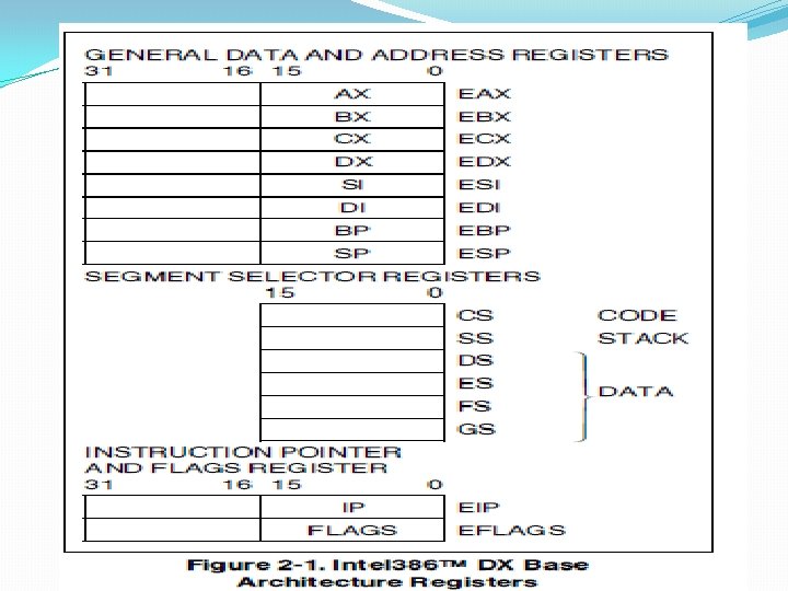
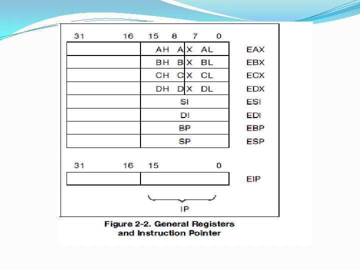
Register Set The Intel 386 DX has 32 register resources in the following categories: � General Purpose Registers � Segment Registers � Instruction Pointer and Flags � Control Registers � System Address Registers � Debug Registers � Test Registers.

�registers are a superset of the 8086, 80186 and 80286 registers, � all 16 -bit 8086, 80186 and 80286 registers are contained within the 32 -bit Intel 386

Flag Registers

Segment Registers

Control Register

System Address Register

Debug and Test Registers
- Slides: 32