UNIT8 LOGIC GATES Logic Gates Types of Gates
- Slides: 22

UNIT-8 LOGIC GATES

Logic Gates Types of Gates: • 1) OR Gate • • • 2) AND Gate 3) NOT Gate 4) NAND Gate 5) NOR Gate 6) EX-OR Gate 7) EX-NOR Gate

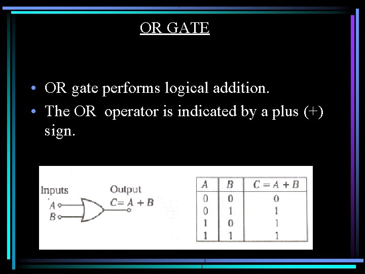
OR GATE • OR gate performs logical addition. • The OR operator is indicated by a plus (+) sign.

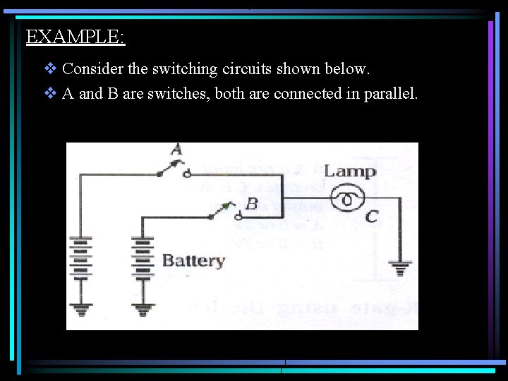
EXAMPLE: v Consider the switching circuits shown below. v A and B are switches, both are connected in parallel.

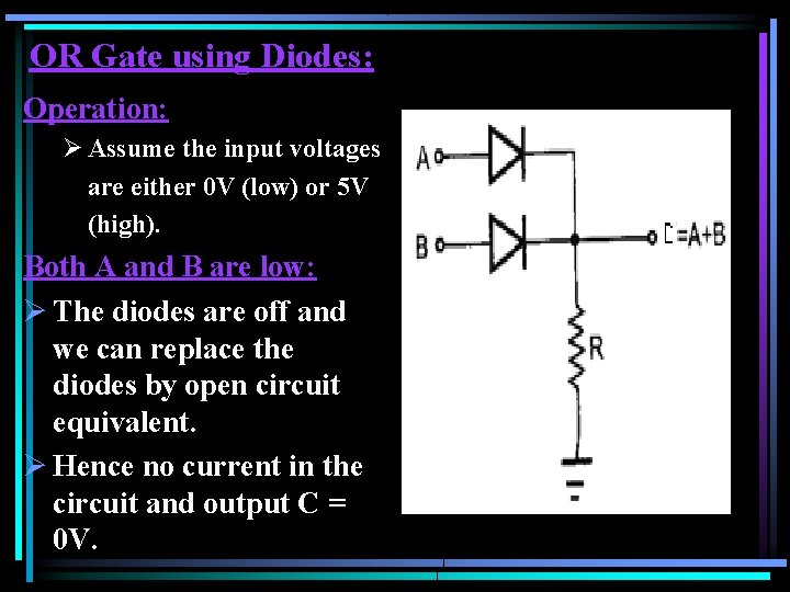
OR Gate using Diodes: Operation: Ø Assume the input voltages are either 0 V (low) or 5 V (high). Both A and B are low: Ø The diodes are off and we can replace the diodes by open circuit equivalent. Ø Hence no current in the circuit and output C = 0 V.

A is low and B is high: • When A is low the corresponding diode will be off and, B is high so the diode corresponds to the input B will be ON. • Now we can replace the ON diode by the short circuit equivalent and the output C=5 V.

• B is low and A is high: – When B is low the corresponding diode will be off and, A is high so the diode corresponds to the input A will be ON. – Now we can replace the ON diode by the short circuit equivalent and the output C=5 V.

• Both A and B are high: – When both the inputs are high both the diodes will be ON and the output C=5 V.

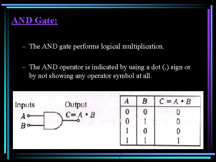
AND Gate: – The AND gate performs logical multiplication. – The AND operator is indicated by using a dot (. ) sign or by not showing any operator symbol at all.

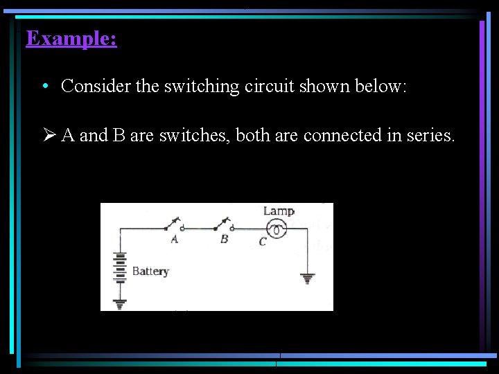
Example: • Consider the switching circuit shown below: Ø A and B are switches, both are connected in series.

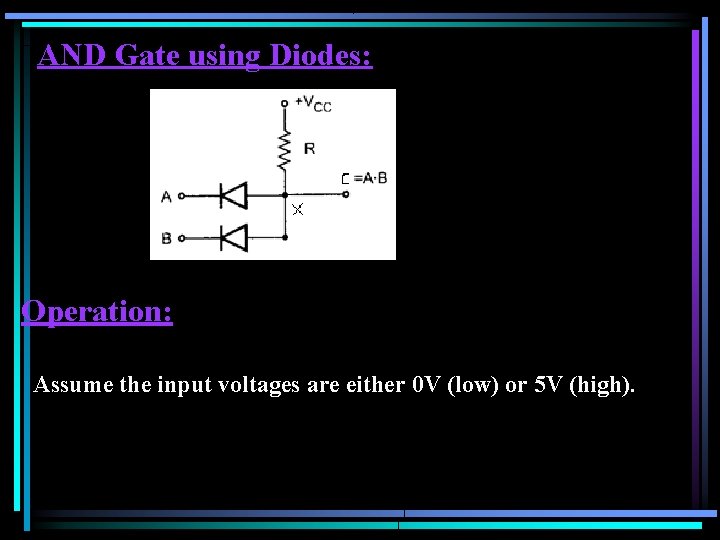
AND Gate using Diodes: Operation: Assume the input voltages are either 0 V (low) or 5 V (high).

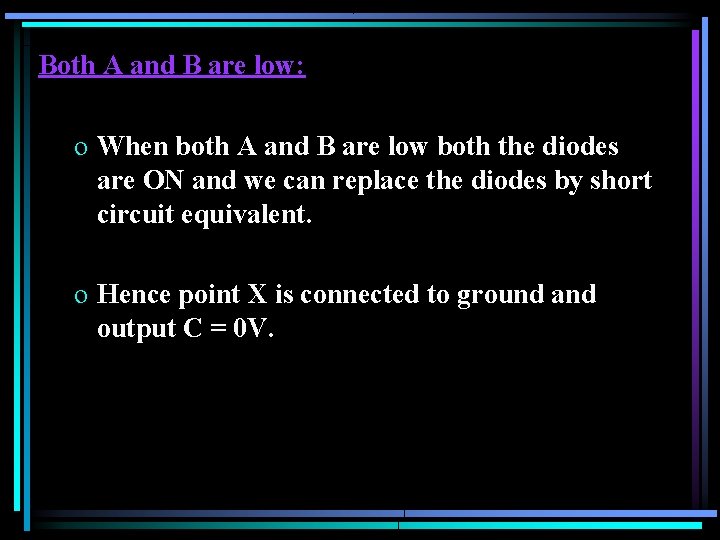
Both A and B are low: o When both A and B are low both the diodes are ON and we can replace the diodes by short circuit equivalent. o Hence point X is connected to ground and output C = 0 V.

A is low and B is high: o When A is low the corresponding diode will be ON and, B is high so the diode corresponds to the input B will be OFF. o Now we can replace the ON diode by the short circuit equivalent; hence point X is connected to ground and the output C=0 V.

B is low and A is high: o When B is low the corresponding diode will be ON and, A is high so the diode corresponds to the input A will be OFF. o Now we can replace the ON diode by the short circuit equivalent; hence point X is connected to ground and the output C=0 V. Both A and B are high: o Both the diodes will be OFF and the output C=5 V.

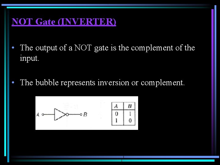
NOT Gate (INVERTER) • The output of a NOT gate is the complement of the input. • The bubble represents inversion or complement.

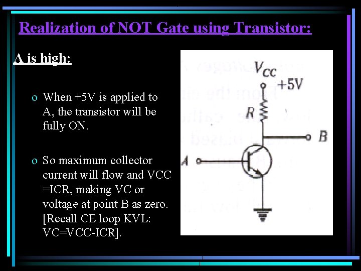
Realization of NOT Gate using Transistor: A is high: o When +5 V is applied to A, the transistor will be fully ON. o So maximum collector current will flow and VCC =ICR, making VC or voltage at point B as zero. [Recall CE loop KVL: VC=VCC-ICR].

A is low: o When 0 V is applied to A, the transistor will be cut-off. o So IC=0 m. A and VC or voltage at point B is equal to VCC.

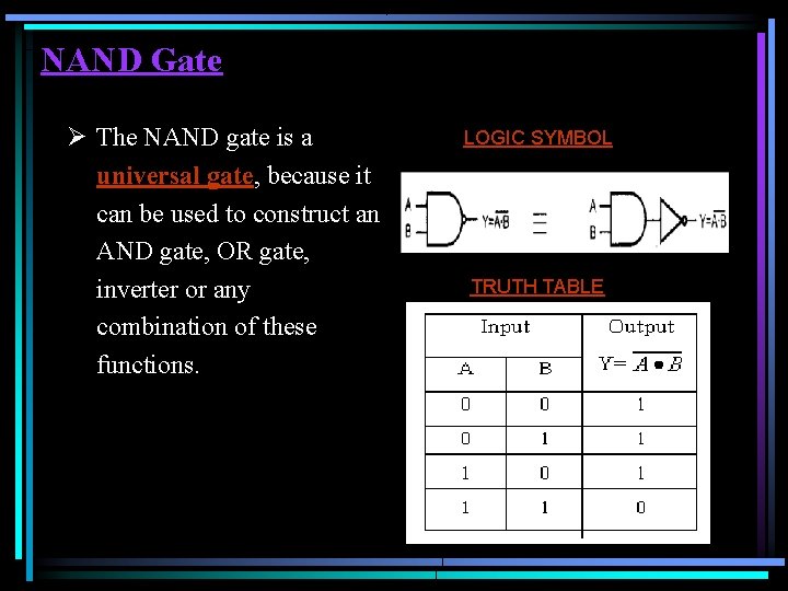
NAND Gate Ø The NAND gate is a universal gate, because it can be used to construct an AND gate, OR gate, inverter or any combination of these functions. LOGIC SYMBOL TRUTH TABLE

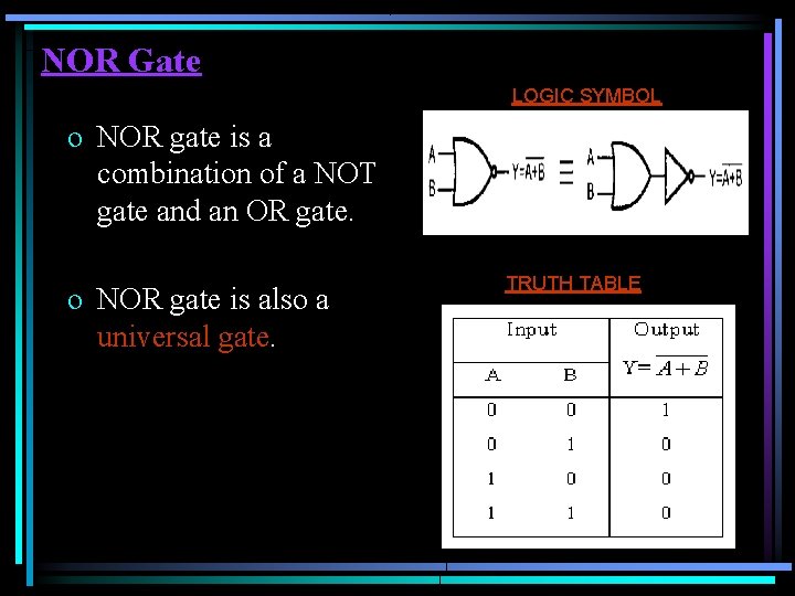
NOR Gate LOGIC SYMBOL o NOR gate is a combination of a NOT gate and an OR gate. o NOR gate is also a universal gate. TRUTH TABLE

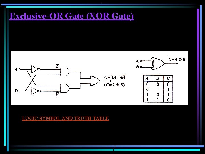
Exclusive-OR Gate (XOR Gate) LOGIC SYMBOL AND TRUTH TABLE

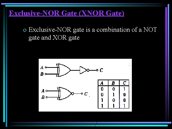
Exclusive-NOR Gate (XNOR Gate) o Exclusive-NOR gate is a combination of a NOT gate and XOR gate

Boolean algebra: o Boolean algebra is a system of mathematical logic. o It has two values 0 and 1. o It differs from both ordinary algebra and binary number system. For example: in Boolean, 1+1 = 1; in binary arithmetic 1 + 1 = 10.