Unit7 IO Interfacing Prof Swati Sharma swati sharmadarshan

- Slides: 58

Unit-7 I/O Interfacing Prof. Swati Sharma swati. sharma@darshan. ac. in Microprocessor Unit-6 Stack & Subroutines & Interfacing - 2150707 Darshan Institute of Engineering & Technology

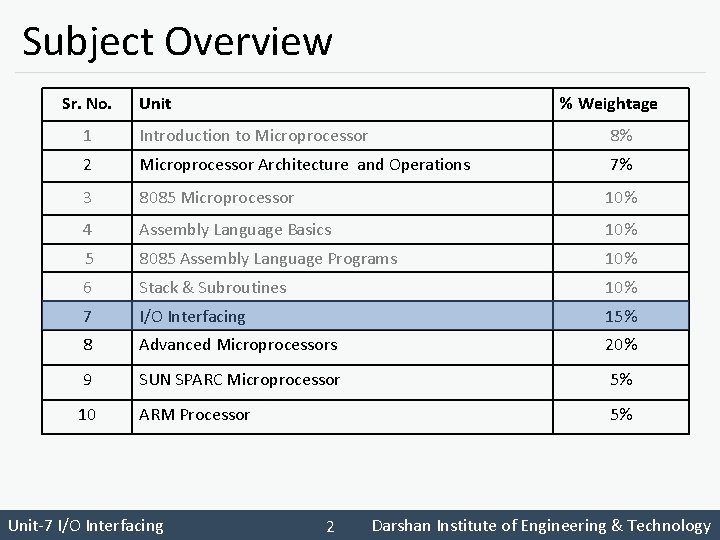
Subject Overview Sr. No. Unit % Weightage 1 Introduction to Microprocessor 8% 2 Microprocessor Architecture and Operations 7% 3 8085 Microprocessor 10% 4 Assembly Language Basics 10% 5 8085 Assembly Language Programs 10% 6 Stack & Subroutines 10% 7 I/O Interfacing 15% 8 Advanced Microprocessors 20% 9 SUN SPARC Microprocessor 5% 10 ARM Processor 5% Unit-7 I/O Interfacing 2 Darshan Institute of Engineering & Technology

Introduction § Interface is the path for communication between two components. § Interfacing is of two types, memory interfacing and I/O interfacing. IO Interfacing What do you mean by I/O Interfacing? § There are various communication devices like the keyboard, mouse, printer, etc. § So, we need to interface the keyboard and other devices with the microprocessor by using latches and buffers. § This type of interfacing is known as I/O interfacing. Unit-7 I/O Interfacing 3 Darshan Institute of Engineering & Technology

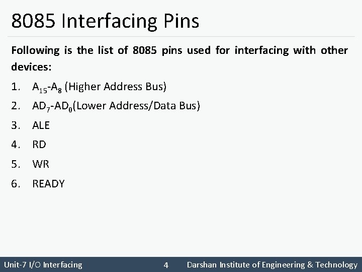
8085 Interfacing Pins Following is the list of 8085 pins used for interfacing with other devices: 1. A 15 -A 8 (Higher Address Bus) 2. AD 7 -AD 0(Lower Address/Data Bus) 3. ALE 4. RD 5. WR 6. READY Unit-7 I/O Interfacing 4 Darshan Institute of Engineering & Technology

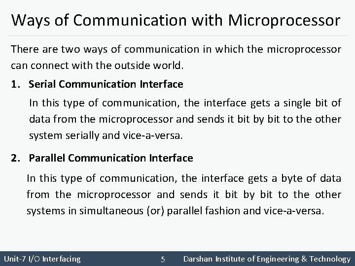
Ways of Communication with Microprocessor There are two ways of communication in which the microprocessor can connect with the outside world. 1. Serial Communication Interface In this type of communication, the interface gets a single bit of data from the microprocessor and sends it by bit to the other system serially and vice-a-versa. 2. Parallel Communication Interface In this type of communication, the interface gets a byte of data from the microprocessor and sends it by bit to the other systems in simultaneous (or) parallel fashion and vice-a-versa. Unit-7 I/O Interfacing 5 Darshan Institute of Engineering & Technology

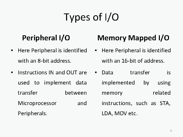
Types of I/O Peripheral I/O Memory Mapped I/O • Here Peripheral is identified with an 8 -bit address. • Here Peripheral is identified with an 16 -bit of address. • Instructions IN and OUT are • Data transfer used to implement data implemented transfer memory Microprocessor Peripherals. between and by is using related instructions, such as STA, LDA, MOV etc. 6

Interrupts in 8085 Unit-6 Stack & Subroutines Darshan Institute of Engineering & Technology

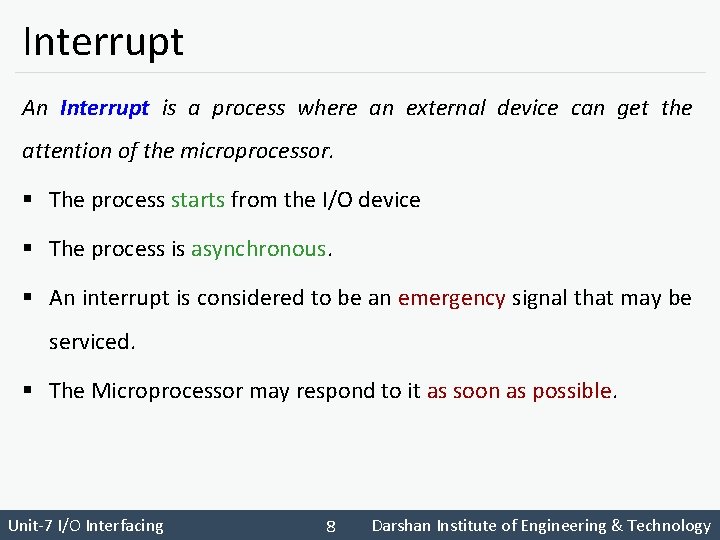
Interrupt An Interrupt is a process where an external device can get the attention of the microprocessor. § The process starts from the I/O device § The process is asynchronous. § An interrupt is considered to be an emergency signal that may be serviced. § The Microprocessor may respond to it as soon as possible. Unit-7 I/O Interfacing 8 Darshan Institute of Engineering & Technology

Interrupt What happens when Microprocessor is interrupted ? § When the Microprocessor receives an interrupt signal, it suspends the currently executing program and jumps to an Interrupt Service Routine (ISR) to respond to the incoming interrupt. § Each interrupt will most probably have its own ISR. Unit-7 I/O Interfacing 9 Darshan Institute of Engineering & Technology

Interrupt Responding to Interrupts § Responding to an interrupt may be immediate or delayed depending on whether the interrupt is maskable or non-maskable and whether interrupts are being masked or not. Unit-7 I/O Interfacing 10 Darshan Institute of Engineering & Technology

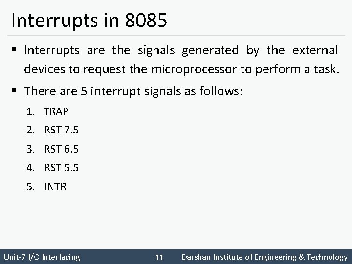
Interrupts in 8085 § Interrupts are the signals generated by the external devices to request the microprocessor to perform a task. § There are 5 interrupt signals as follows: 1. TRAP 2. RST 7. 5 3. RST 6. 5 4. RST 5. 5 5. INTR Unit-7 I/O Interfacing 11 Darshan Institute of Engineering & Technology

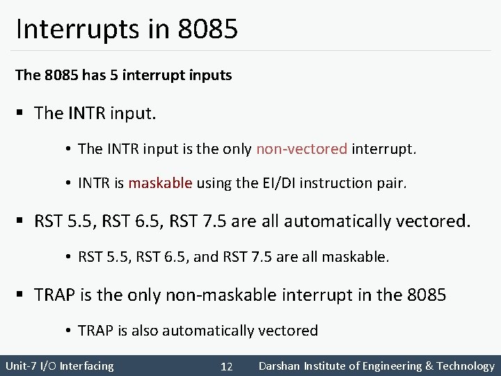
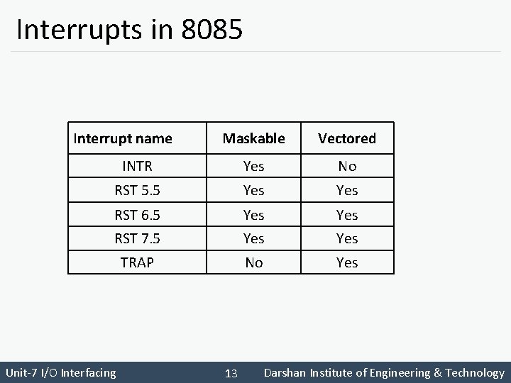
Interrupts in 8085 The 8085 has 5 interrupt inputs § The INTR input. • The INTR input is the only non-vectored interrupt. • INTR is maskable using the EI/DI instruction pair. § RST 5. 5, RST 6. 5, RST 7. 5 are all automatically vectored. • RST 5. 5, RST 6. 5, and RST 7. 5 are all maskable. § TRAP is the only non-maskable interrupt in the 8085 • TRAP is also automatically vectored Unit-7 I/O Interfacing 12 Darshan Institute of Engineering & Technology

Interrupts in 8085 Interrupt name Maskable Vectored INTR Yes No RST 5. 5 Yes RST 6. 5 Yes RST 7. 5 Yes TRAP No Yes Unit-7 I/O Interfacing 13 Darshan Institute of Engineering & Technology

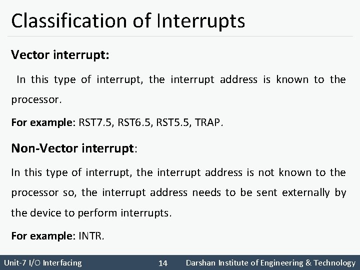
Classification of Interrupts Vector interrupt: In this type of interrupt, the interrupt address is known to the processor. For example: RST 7. 5, RST 6. 5, RST 5. 5, TRAP. Non-Vector interrupt: In this type of interrupt, the interrupt address is not known to the processor so, the interrupt address needs to be sent externally by the device to perform interrupts. For example: INTR. Unit-7 I/O Interfacing 14 Darshan Institute of Engineering & Technology

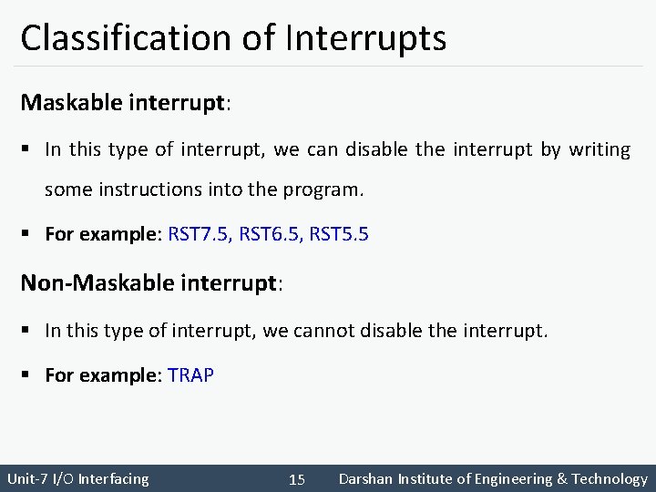
Classification of Interrupts Maskable interrupt: § In this type of interrupt, we can disable the interrupt by writing some instructions into the program. § For example: RST 7. 5, RST 6. 5, RST 5. 5 Non-Maskable interrupt: § In this type of interrupt, we cannot disable the interrupt. § For example: TRAP Unit-7 I/O Interfacing 15 Darshan Institute of Engineering & Technology

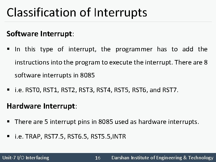
Classification of Interrupts Software Interrupt: § In this type of interrupt, the programmer has to add the instructions into the program to execute the interrupt. There are 8 software interrupts in 8085 § i. e. RST 0, RST 1, RST 2, RST 3, RST 4, RST 5, RST 6, and RST 7. Hardware Interrupt: § There are 5 interrupt pins in 8085 used as hardware interrupts. § i. e. TRAP, RST 7. 5, RST 6. 5, RST 5. 5, INTR Unit-7 I/O Interfacing 16 Darshan Institute of Engineering & Technology

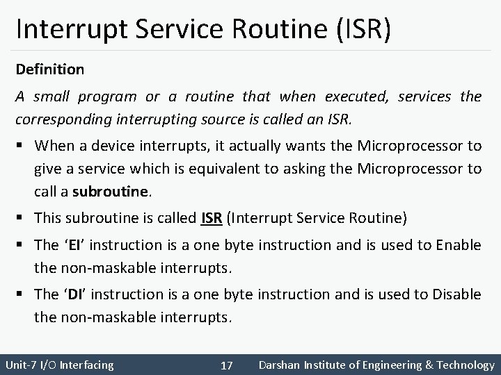
Interrupt Service Routine (ISR) Definition A small program or a routine that when executed, services the corresponding interrupting source is called an ISR. § When a device interrupts, it actually wants the Microprocessor to give a service which is equivalent to asking the Microprocessor to call a subroutine. § This subroutine is called ISR (Interrupt Service Routine) § The ‘EI’ instruction is a one byte instruction and is used to Enable the non-maskable interrupts. § The ‘DI’ instruction is a one byte instruction and is used to Disable the non-maskable interrupts. Unit-7 I/O Interfacing 17 Darshan Institute of Engineering & Technology

Programmable Peripheral Interface 8255 A Unit-6 Stack & Subroutines Darshan Institute of Engineering & Technology

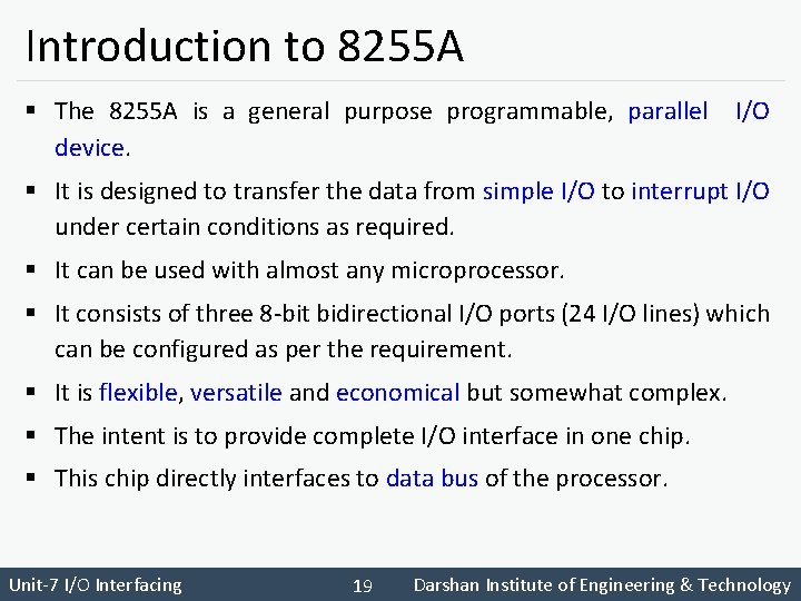
Introduction to 8255 A § The 8255 A is a general purpose programmable, parallel device. I/O § It is designed to transfer the data from simple I/O to interrupt I/O under certain conditions as required. § It can be used with almost any microprocessor. § It consists of three 8 -bit bidirectional I/O ports (24 I/O lines) which can be configured as per the requirement. § It is flexible, versatile and economical but somewhat complex. § The intent is to provide complete I/O interface in one chip. § This chip directly interfaces to data bus of the processor. Unit-7 I/O Interfacing 19 Darshan Institute of Engineering & Technology

Block diagram of 8255 A Unit-6 Stack & Subroutines Darshan Institute of Engineering & Technology

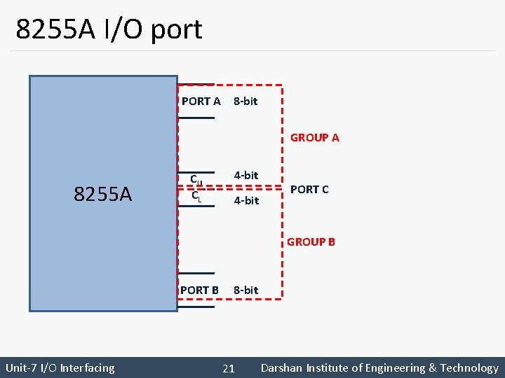
8255 A I/O port PORT A 8 -bit GROUP A 8255 A CU CL 4 -bit PORT C GROUP B PORT B Unit-7 I/O Interfacing 8 -bit 21 Darshan Institute of Engineering & Technology

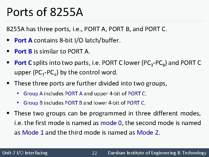
Ports of 8255 A has three ports, i. e. , PORT A, PORT B, and PORT C. § Port A contains 8 -bit I/O latch/buffer. § Port B is similar to PORT A. § Port C splits into two parts, i. e. PORT C lower (PC 3 -PC 0) and PORT C upper (PC 7 -PC 4) by the control word. § These three ports are further divided into two groups, • Group A includes PORT A and upper 4 -bit of PORT C. • Group B includes PORT B and lower 4 -bit of PORT C. § These two groups can be programmed in three different modes, i. e. the first mode is named as mode 0, the second mode is named as Mode 1 and the third mode is named as Mode 2. Unit-7 I/O Interfacing 22 Darshan Institute of Engineering & Technology

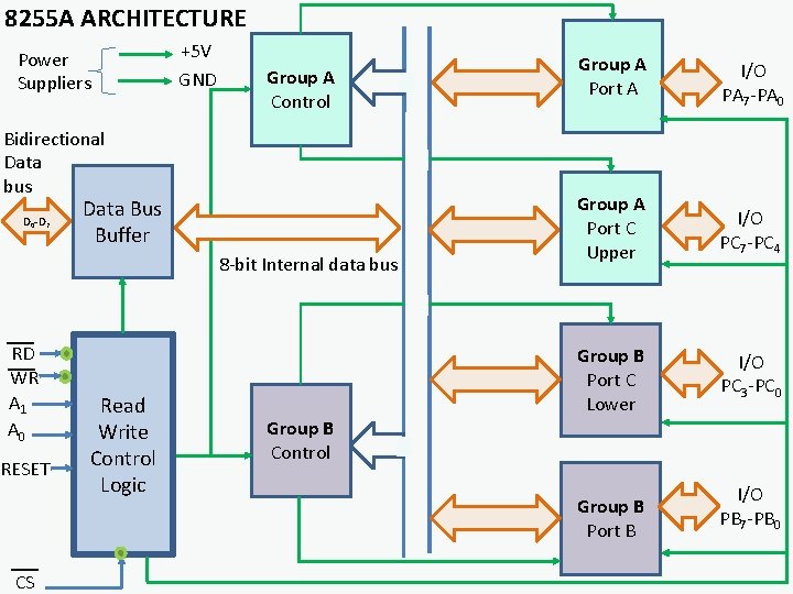
8255 A ARCHITECTURE Power Suppliers +5 V GND Group A Control Bidirectional Data bus D 0 -D 7 Data Bus Buffer 8 -bit Internal data bus RD WR A 1 A 0 RESET CS Read Write Control Logic Group A Port A I/O PA 7 -PA 0 Group A Port C Upper I/O PC 7 -PC 4 Group B Port C Lower I/O PC 3 -PC 0 Group B Control Group B Port B I/O PB 7 -PB 0

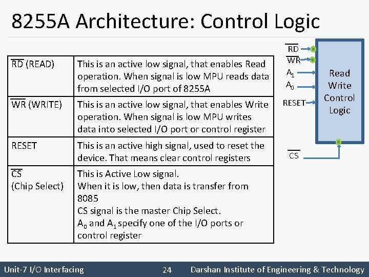
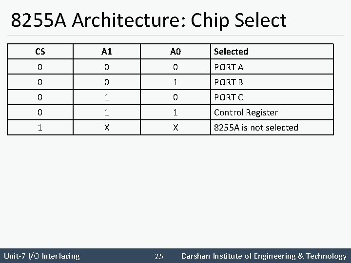
8255 A Architecture: Control Logic RD (READ) This is an active low signal, that enables Read operation. When signal is low MPU reads data from selected I/O port of 8255 A WR (WRITE) This is an active low signal, that enables Write operation. When signal is low MPU writes data into selected I/O port or control register RESET This is an active high signal, used to reset the device. That means clear control registers CS (Chip Select) This is Active Low signal. When it is low, then data is transfer from 8085 CS signal is the master Chip Select. A 0 and A 1 specify one of the I/O ports or control register Unit-7 I/O Interfacing 24 RD WR A 1 A 0 RESET Read Write Control Logic CS Darshan Institute of Engineering & Technology

8255 A Architecture: Chip Select CS A 1 A 0 Selected 0 0 0 PORT A 0 0 1 PORT B 0 1 0 PORT C 0 1 1 Control Register 1 X X 8255 A is not selected Unit-7 I/O Interfacing 25 Darshan Institute of Engineering & Technology

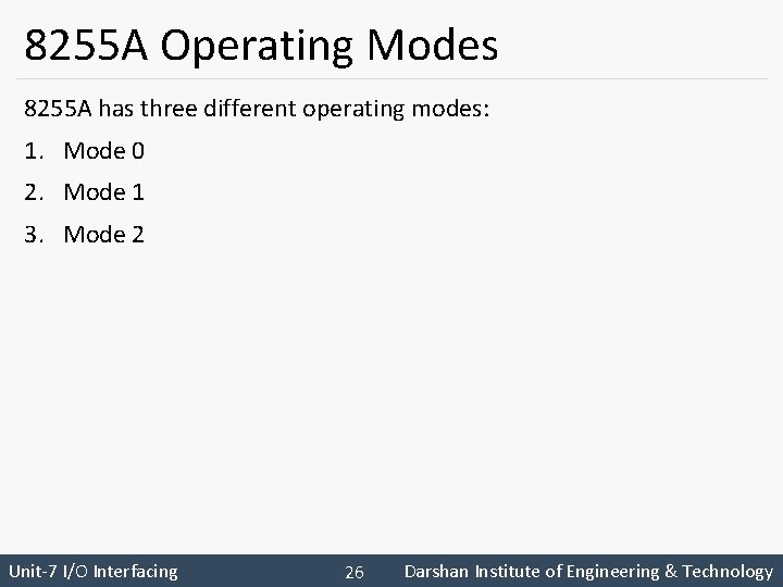
8255 A Operating Modes 8255 A has three different operating modes: 1. Mode 0 2. Mode 1 3. Mode 2 Unit-7 I/O Interfacing 26 Darshan Institute of Engineering & Technology

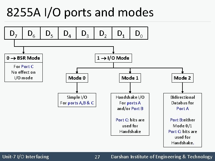
8255 A I/O ports and modes D 7 D 6 D 5 D 4 D 3 0 BSR Mode For Port C No effect on I/O mode Unit-7 I/O Interfacing D 2 D 1 D 0 1 I/O Mode 0 Mode 1 Mode 2 Simple I/O For ports A, B & C Handshake I/O For ports A and/or Port B Bidirectional Databus for Port A Port C: bits are used for Handshake Port B: either Mode 0/1 Port C: bits are used for Handshake. 27 Darshan Institute of Engineering & Technology

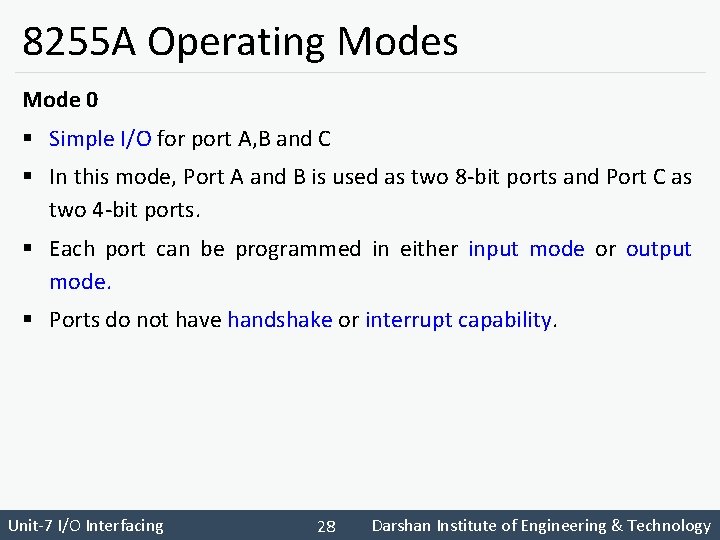
8255 A Operating Modes Mode 0 § Simple I/O for port A, B and C § In this mode, Port A and B is used as two 8 -bit ports and Port C as two 4 -bit ports. § Each port can be programmed in either input mode or output mode. § Ports do not have handshake or interrupt capability. Unit-7 I/O Interfacing 28 Darshan Institute of Engineering & Technology

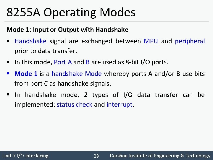
8255 A Operating Modes Mode 1: Input or Output with Handshake § Handshake signal are exchanged between MPU and peripheral prior to data transfer. § In this mode, Port A and B are used as 8 -bit I/O ports. § Mode 1 is a handshake Mode whereby ports A and/or B use bits from port C as handshake signals. § In handshake mode, 2 types of I/O data transfer can be implemented: status check and interrupt. Unit-7 I/O Interfacing 29 Darshan Institute of Engineering & Technology

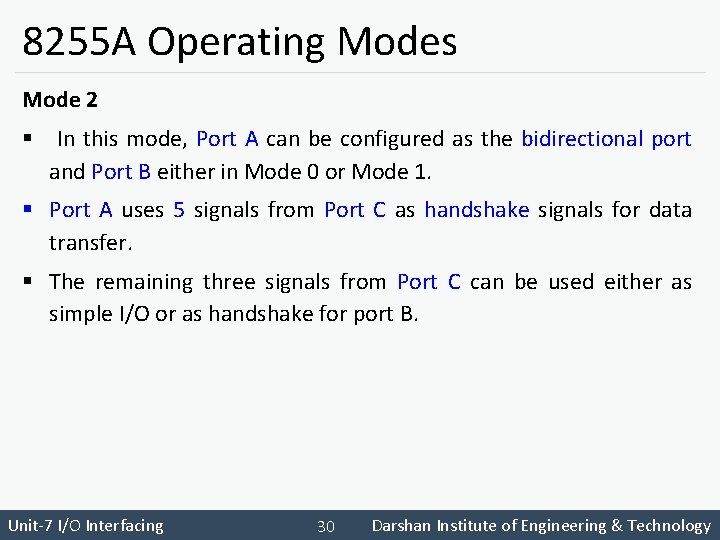
8255 A Operating Modes Mode 2 § In this mode, Port A can be configured as the bidirectional port and Port B either in Mode 0 or Mode 1. § Port A uses 5 signals from Port C as handshake signals for data transfer. § The remaining three signals from Port C can be used either as simple I/O or as handshake for port B. Unit-7 I/O Interfacing 30 Darshan Institute of Engineering & Technology

Features of 8255 A The prominent features of 8255 A are as follows: § It consists of three 8 -bit IO ports i. e. PA, PB, and PC. § Address/data bus must be externally demultiplexed. § It has improved DC driving capability. Unit-7 I/O Interfacing 31 Darshan Institute of Engineering & Technology

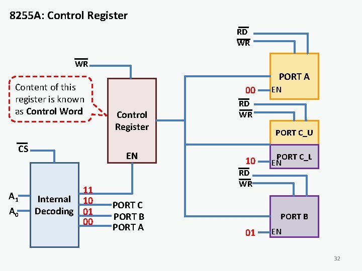
8255 A: Control Register RD WR WR Content of this register is known as Control Word CS A 1 A 0 PORT A 00 Control Register EN 11 Internal 10 Decoding 01 00 RD WR PORT C_U 10 RD WR PORT C PORT B PORT A EN PORT C_L EN PORT B 01 EN 32

8255 A: Control Word § Accessed to write a control word when A 0 and A 1 are at logic 1. To communicate with peripherals through the 8255 A, three steps are necessary: 1. Determine the addresses of ports A, B, and C and of the control register according to the Chip select logic and address lines A 0 and A 1. 2. Write a control word in the control register. 3. Write I/O instructions to communicate with peripherals through ports A, B, and C Unit-7 I/O Interfacing 33 Darshan Institute of Engineering & Technology

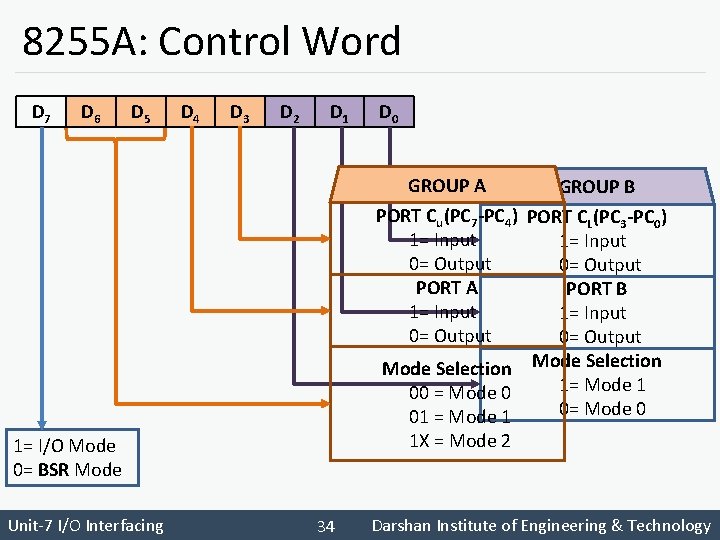
8255 A: Control Word D 7 D 6 D 5 D 4 D 3 D 2 D 1 D 0 GROUP A GROUP B PORT Cu(PC 7 -PC 4) PORT CL(PC 3 -PC 0) 1= Input 0= Output PORT A PORT B 1= Input 0= Output Mode Selection 1= Mode 1 00 = Mode 0 01 = Mode 1 1 X = Mode 2 1= I/O Mode 0= BSR Mode Unit-7 I/O Interfacing 34 Darshan Institute of Engineering & Technology

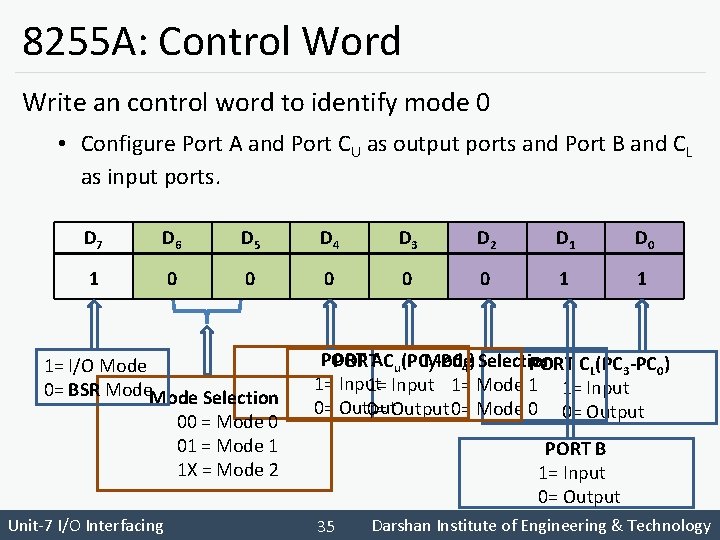
8255 A: Control Word Write an control word to identify mode 0 • Configure Port A and Port CU as output ports and Port B and CL as input ports. D 7 D 6 D 5 D 4 D 3 D 2 D 1 D 0 1 0 0 0 1 1 1= I/O Mode 0= BSR Mode Selection 00 = Mode 0 01 = Mode 1 1 X = Mode 2 Unit-7 I/O Interfacing PORTACu(PCMode PORT CL(PC 3 -PC 0) 7 -PC 4) Selection 1= Input 1= Mode 1 1= Input 0= Output 0= Mode 0 0= Output PORT B 1= Input 0= Output 35 Darshan Institute of Engineering & Technology

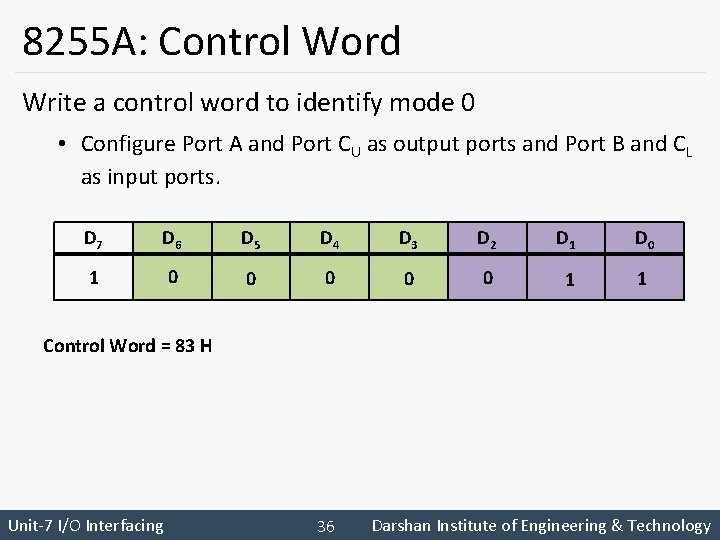
8255 A: Control Word Write a control word to identify mode 0 • Configure Port A and Port CU as output ports and Port B and CL as input ports. D 7 D 6 D 5 D 4 D 3 D 2 D 1 D 0 1 0 0 0 1 1 Control Word = 83 H Unit-7 I/O Interfacing 36 Darshan Institute of Engineering & Technology

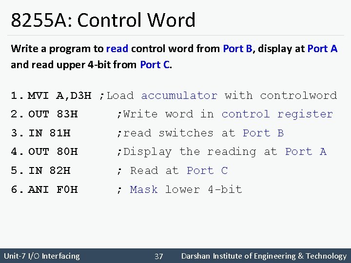
8255 A: Control Word Write a program to read control word from Port B, display at Port A and read upper 4 -bit from Port C. 1. MVI A, D 3 H ; Load accumulator with controlword 2. OUT 83 H ; Write word in control register 3. IN 81 H ; read switches at Port B 4. OUT 80 H ; Display the reading at Port A 5. IN 82 H ; Read at Port C 6. ANI F 0 H ; Mask lower 4 -bit Unit-7 I/O Interfacing 37 Darshan Institute of Engineering & Technology

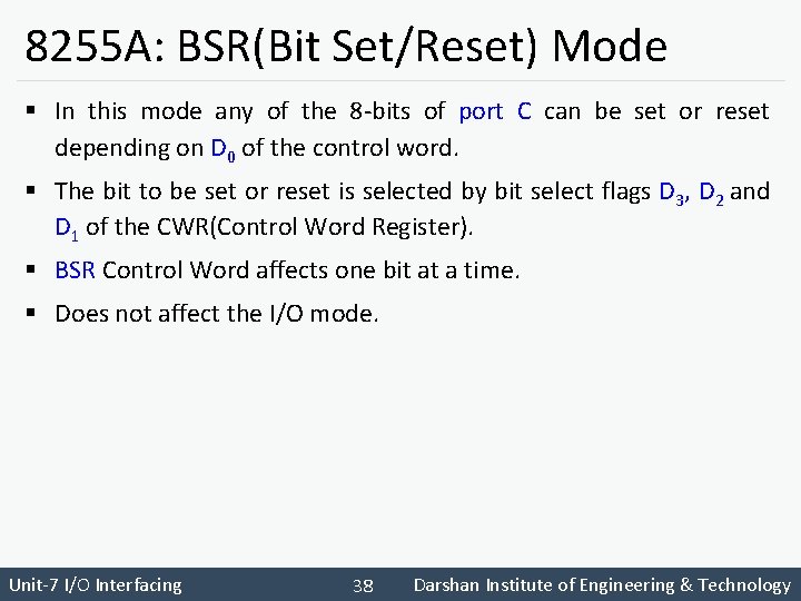
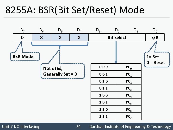
8255 A: BSR(Bit Set/Reset) Mode § In this mode any of the 8 -bits of port C can be set or reset depending on D 0 of the control word. § The bit to be set or reset is selected by bit select flags D 3, D 2 and D 1 of the CWR(Control Word Register). § BSR Control Word affects one bit at a time. § Does not affect the I/O mode. Unit-7 I/O Interfacing 38 Darshan Institute of Engineering & Technology

8255 A: BSR(Bit Set/Reset) Mode D 7 D 6 D 5 D 4 0 X X X D 3 D 2 D 1 Bit Select BSR Mode Not used, Generally Set = 0 Unit-7 I/O Interfacing 39 000 PC 0 001 PC 1 010 PC 2 011 PC 3 100 PC 4 101 PC 5 110 PC 6 111 PC 7 D 0 S/R 1= Set 0 = Reset Darshan Institute of Engineering & Technology

Programmable Interrupt Controller 8259 A Unit-6 Stack & Subroutines Darshan Institute of Engineering & Technology

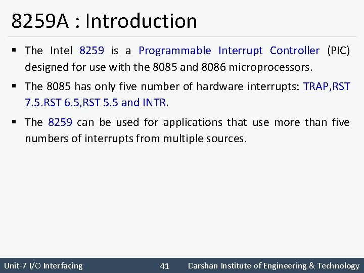
8259 A : Introduction § The Intel 8259 is a Programmable Interrupt Controller (PIC) designed for use with the 8085 and 8086 microprocessors. § The 8085 has only five number of hardware interrupts: TRAP, RST 7. 5. RST 6. 5, RST 5. 5 and INTR. § The 8259 can be used for applications that use more than five numbers of interrupts from multiple sources. Unit-7 I/O Interfacing 41 Darshan Institute of Engineering & Technology

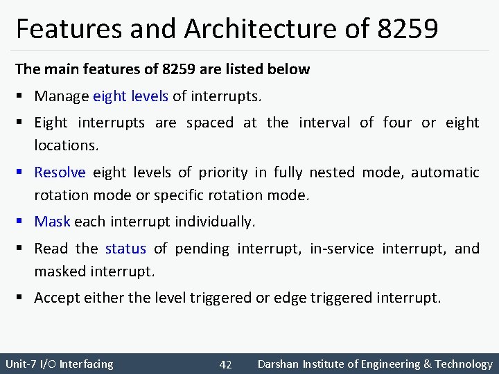
Features and Architecture of 8259 The main features of 8259 are listed below § Manage eight levels of interrupts. § Eight interrupts are spaced at the interval of four or eight locations. § Resolve eight levels of priority in fully nested mode, automatic rotation mode or specific rotation mode. § Mask each interrupt individually. § Read the status of pending interrupt, in-service interrupt, and masked interrupt. § Accept either the level triggered or edge triggered interrupt. Unit-7 I/O Interfacing 42 Darshan Institute of Engineering & Technology

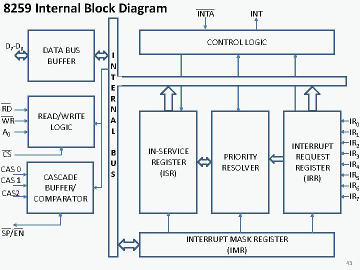
8259 Internal Block Diagram D 7 -D 0 RD WR A 0 DATA BUS BUFFER READ/WRITE LOGIC CS CAS 0 CAS 1 CAS 2 SP/EN CASCADE BUFFER/ COMPARATOR INTA INT CONTROL LOGIC I N T E R N A L B U S IN-SERVICE REGISTER (ISR) PRIORITY RESOLVER INTERRUPT REQUEST REGISTER (IRR) IR 0 IR 1 IR 2 IR 3 IR 4 IR 5 IR 6 IR 7 INTERRUPT MASK REGISTER (IMR) 43

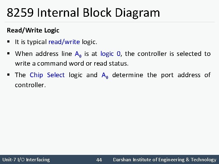
8259 Internal Block Diagram Read/Write Logic § It is typical read/write logic. § When address line A 0 is at logic 0, the controller is selected to write a command word or read status. § The Chip Select logic and A 0 determine the port address of controller. Unit-7 I/O Interfacing 44 Darshan Institute of Engineering & Technology

8259 Internal Block Diagram Control Logic § It has two pins: INT as output and INTA as input. § The INT is connected to INTR pin of MPU. Unit-7 I/O Interfacing 45 Darshan Institute of Engineering & Technology

8259 Internal Block Diagram Interrupt Registers and Priority Resolver 1. Interrupt Request Register (IRR) 2. Interrupt In-Service Register (ISR) 3. Priority Resolver 4. Interrupt Mask Register (IMR) Unit-7 I/O Interfacing 46 Darshan Institute of Engineering & Technology

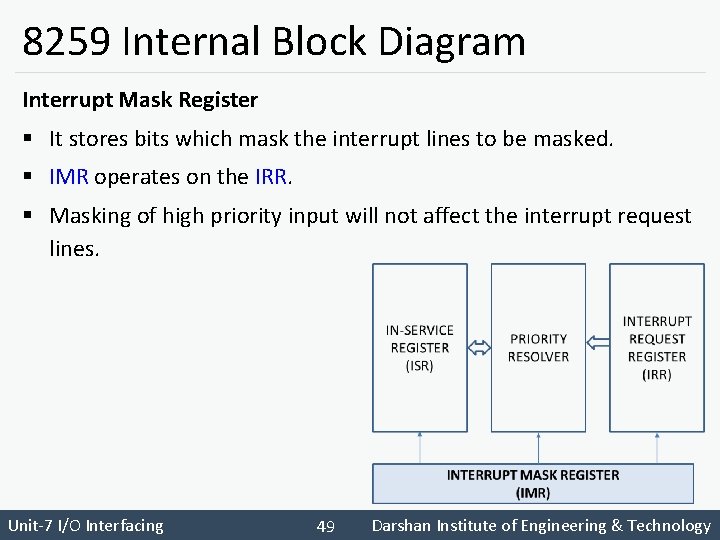
8259 Internal Block Diagram Interrupt Request Register (IRR) and Interrupt In-Service Register (ISR) § Interrupt input lines are handled by two registers in cascade – IRR and ISR § IRR is used to store all interrupt which are requesting service. § ISR is used to store all interrupts which are being serviced. Unit-7 I/O Interfacing 47 Darshan Institute of Engineering & Technology

8259 Internal Block Diagram Priority Resolver § This logic block determines the priorities of the bit set in IRR. § IR 0 is having highest priority, IR 7 is having lowest priority Unit-7 I/O Interfacing 48 Darshan Institute of Engineering & Technology

8259 Internal Block Diagram Interrupt Mask Register § It stores bits which mask the interrupt lines to be masked. § IMR operates on the IRR. § Masking of high priority input will not affect the interrupt request lines. Unit-7 I/O Interfacing 49 Darshan Institute of Engineering & Technology

8259 Internal Block Diagram Cascade Buffer / Comparator § This block is used to expand the number of interrupt levels by cascading two or more 8259 As. Unit-7 I/O Interfacing 50 Darshan Institute of Engineering & Technology

INTERFACING WITH SEVEN SEGMENT DISPLAY LED Unit-6 Stack & Subroutines Darshan Institute of Engineering & Technology

Interfacing with seven segment § Interface the 8085 Microprocessor System with seven segment display through its programmable I/O port 8255. § Seven segment displays is often used in the digital electronic equipment to display information regarding certain process. Unit-7 I/O Interfacing 52 Darshan Institute of Engineering & Technology

Basic Concepts in I/O Interfacing § I/O devices (or peripherals) such as LEDs and keyboards are essential components of the microprocessor-based or microcontroller-based systems. § Classified into two groups 1. input devices 2. output devices Unit-7 I/O Interfacing 53 Darshan Institute of Engineering & Technology

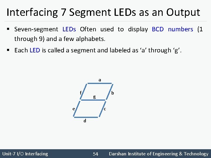
Interfacing 7 Segment LEDs as an Output § Seven-segment LEDs Often used to display BCD numbers (1 through 9) and a few alphabets. § Each LED is called a segment and labeled as ‘a’ through ‘g’. a f b g e c d Unit-7 I/O Interfacing 54 Darshan Institute of Engineering & Technology

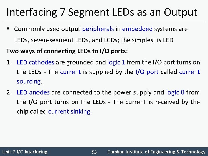
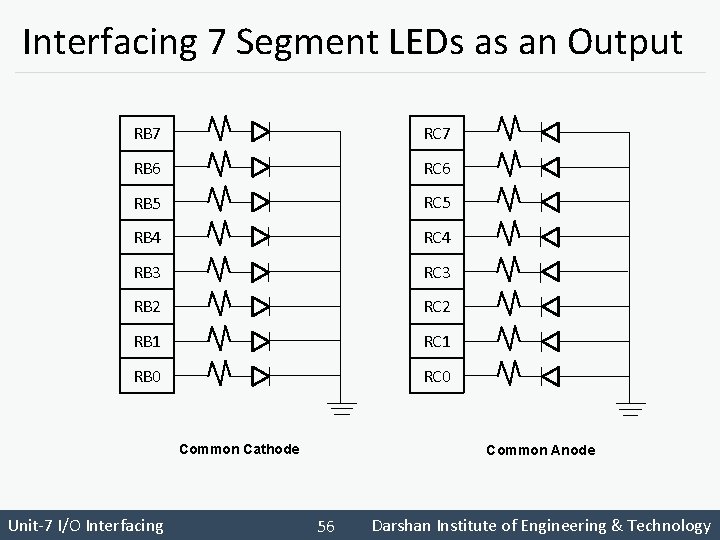
Interfacing 7 Segment LEDs as an Output § Commonly used output peripherals in embedded systems are LEDs, seven-segment LEDs, and LCDs; the simplest is LED Two ways of connecting LEDs to I/O ports: 1. LED cathodes are grounded and logic 1 from the I/O port turns on the LEDs - The current is supplied by the I/O port called current sourcing. 2. LED anodes are connected to the power supply and logic 0 from the I/O port turns on the LEDs - The current is received by the chip called current sinking. Unit-7 I/O Interfacing 55 Darshan Institute of Engineering & Technology

Interfacing 7 Segment LEDs as an Output RB 7 RC 7 RB 6 RC 6 RB 5 RC 5 RB 4 RC 4 RB 3 RC 3 RB 2 RC 2 RB 1 RC 1 RB 0 RC 0 Common Cathode Unit-7 I/O Interfacing Common Anode 56 Darshan Institute of Engineering & Technology

Interfacing Input Peripherals § Commonly used input peripherals in embedded systems are: DIP switches, push-button keys, keyboards, and A/D converters. § DIP switch: One side of the switch is tied high (to a power supply through a resistor called a pull-up resistor), and the other side is grounded. The logic level changes when the position is switched. § Push-button key: The connection is the same as in the DIP switch except that contact is momentary. Unit-7 I/O Interfacing 57 Darshan Institute of Engineering & Technology

Interfacing Push-Button Keys § Electrical connection of a push-button key is same as that of a DIP switch except that the connection is temporary when the key is pressed. § When a key is pressed (or released), mechanical metal contact bounces momentarily and can be read as multiple inputs. § The reading of one contact as multiple inputs can be eliminated by a key-debounce technique, using either hardware or software. Unit-7 I/O Interfacing 58 Darshan Institute of Engineering & Technology