UNIT1 8086 Architecture Microprocessors Introduction Types of Computers


 Decode: The CPU then decodes the instruction fetched from")

 of")


 S 3 -S 6, QS 0 -QS 1 – Status of")


 Bus Interface Unit (BIU) 2)")
 The BIU fetches instructions, reads and writes data, and computes")
 EU tells the BIU where to fetch instructions and data. The")


 • BX – – Base Register Also serves as")

 Contains the resulting sign of an")


 BHE: Combines with A 0 to form the operation for transfer")
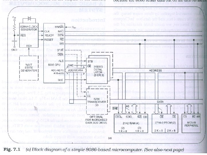


 In Wait State, 8086 will wait for addressed")

 In Wait State, 8086 will wait for addressed")

- Slides: 65
UNIT-1 8086 Architecture
Microprocessors Introduction
Types of Computers Mainframes Super Computers Mini Computers Micro Computers
Mainframes A Mainframe computer is a large, powerful computer that handles the processing for many users simultaneously. Applications: • Processing power and Information storage in a Centralized location • High Capacity Servers. • Military defence control • Graphics displays for Science fiction movies IBM z-series Mainframe
Super Computers A Supercomputer is mainframe computer that has been optimized for High Speed and processing power. Applications: Calculation-intensive tasks such simulating • Nuclear bomb detonations • Aerodynamic flows • Global weather patterns. • 2 -d and 3 -d transient dynamics IBM ASCI White – 12. 3 Trillion operations per sec (Advanced Strategic Computing Initiative)
Mini Computers Scale down version of Mainframe computers are Minicomputers. It is a multi-user computer that is less powerful than a Mainframe Applications: • Business Data Processing • Industrial Control • Scientific Research • Data acquisition • Terminal and peripheral communication control. Apple Mac mini computer
Micro Computers A Microcomputer is a computer that has a microprocessor chip as its CPU. The two types of micro computers are Desktops and Laptops. Desktop personal computer Laptop personal computer
Microcomputer Components CPU – ALU, Control Unit, Registers. Memory – RAM, ROM. Bus – Data, Address, Control Bus. Ports – Input and Output ports. Input – Keyboard, Mouse. Output – Monitor, Printer.
Microcomputer Architecture
Microcomputer Operation A Microcomputer Fetches, Decodes, and Executes an instruction. Fetch Operation: The CPU sends address of required instruction to Memory (port) through address bus. Then Memory (Port) sends the instruction through data bus to the CPU.
Microcomputer Operation (Contd. . ) Decode: The CPU then decodes the instruction fetched from memory. Determines the set of actions. Selects the sequence of microinstructions to be carried out etc. Execute: Finally CPU performs the operation according to the instruction.
Microcomputer Data transfers Memory Read – Memory to CPU. Memory Write – CPU to Memory. Port Read – I/O Port to CPU Port Write – CPU to I/O Port
Microprocessor is an electronic circuit that functions as the central processing unit (CPU) of a computer, providing computational control. Applications: • Smart controllers for graphics displays, storage devices, and high-speed printers. • Controls consumer electronic devices, such as the programmable microwave oven and videocassette recorder. • Regulates gasoline consumption • Monitor alarm systems • Operate automatic tracking and targeting systems in aircraft, tanks, and missiles • Control radar arrays that track and identify aircraft, in defense applications.
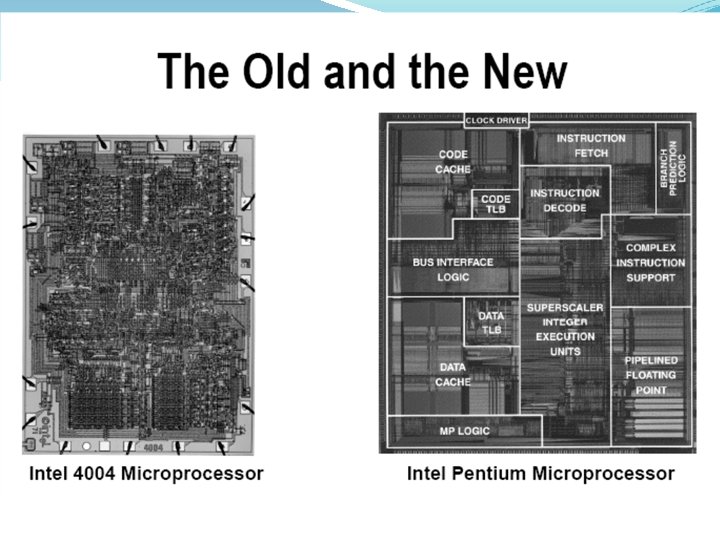
History of Microprocessors Name Date Transistors Microns Clock speed 4004 1971 2, 300 10 0. 1 MHz 8080 1974 6, 000 6 2 MHz 8086 1978 29, 000 3 5 MHz 8088 1979 29, 000 3 5 MHz 80286 1982 134, 000 1. 5 6 MHz 80386 1985 275, 000 1. 5 16 MHz 80486 1989 1, 200, 000 1 25 MHz Pentium 1993 3, 100, 000 0. 8 60 MHz Pentium II 1997 7, 500, 000 0. 35 233 MHz Pentium III 1999 9, 500, 000 0. 25 450 MHz Pentium 4 2000 42, 000 0. 18 1. 5 GHz Pentium 4 "Prescott" 2004 125, 000 0. 09 3. 6 GHz Pentium D processor 2005 291, 000 0. 065 3. 2 GHz Dual Core 2006 1, 720, 000 0. 09 1. 66 Ghz Quad Core Xeon 2007 820, 000 0. 045 3 GHz
Moore’s Law Gordon Moore -- Intel’s co-founder Statement: Transistors on a IC doubles every 2 years.
Microprocessor Components The Main components of Microprocessor are: ALU : – Perform Arithmetic Calculations Control Unit : – Controls other components Registers : – Storing Temporary Data for calculations by ALU Buses : – Data Transfer Between Microprocessor to Memory and I/O
The 8085 Bus Structure The 8 -bit 8085 CPU (or MPU – Micro Processing Unit) communicates with the other units using a 16 -bit address bus, an 8 -bit data bus and a control bus. 18
The 8085 Bus Structure Address Bus § Consists of 16 address lines: A 0 – A 15 § Operates in unidirectional mode: The address the MPU to peripheral devices, not reverse. § 16 address lines are capable of addressing a total of 216 = 65, 536 (64 k) memory locations. § Address locations: 0000 (hex) – FFFF (hex) 19 bits are always sent from
The 8085 Bus Structure Data Bus § Consists of 8 data lines: D 0 – D 7 § Operates in bidirectional mode: The data bits are sent from the MPU to peripheral devices, as well as from the peripheral devices to the MPU. § Data range: 00 (hex) – FF (hex) Control Bus § Consists of various lines carrying the control write enable, flag bits. 20 signals such as read /
The 8085: CPU Internal Structure The internal architecture of the 8085 CPU is capable of performing the following operations: § Store 8 -bit data (Registers, Accumulator) § Perform arithmetic and logic operations (ALU) § Test for conditions (IF / THEN) § Sequence the execution of instructions § Store temporary data in RAM during execution 21
The 8085: CPU Internal Structure Simplified block diagram 22
The 8085: Registers 23
The 8085: CPU Internal Structure Registers § Six general purpose 8 -bit registers: B, C, D, E, H, L § They can also be combined as register pairs to perform 16 -bit operations: BC, DE, HL § Registers are programmable (data load, move, etc. ) Accumulator § Single 8 -bit register that is part of the ALU ! § Used for arithmetic / logic operations – the result is the accumulator. 24 always stored in
The 8085: CPU Internal Structure Flag Bits § Indicate the result of condition tests. § Carry, Zero, Sign, Parity, etc. § Conditional operations (IF / THEN) are executed based on the condition of these flag bits. Program Counter (PC) § Contains the memory address (16 bits) of the executed in the next step. Stack Pointer (SP) 25 instruction that will be
8086 Microprocessor
Microprocessors Family 8086 Family: 8086: First 16 -bit processor 80186: 16 -bit 8086 with peripheral devices 80286: Advanced version of 8086 used for multitasking. 80386: 32 -bit processor architecture 80486: 32 -bit processor architecture with floating point processor(80387) integrated into the chip. 8088 Family: 8088: Same as 8086 but 8 -bit databus. 80188: 8088 with peripheral devices.
8086 Pin Diagram
Pin Description AD 0 -AD 15: Multiplexed Address/Data Bus RD’: Low while reading from memory or port WR’ : Low while writing to memory or port. M/IO’ : High during Memory operations. Low during Port operations. S 0 -S 2 – Bus Control, INTA, I/O read, I/O write, HALT, code access, memory read, memory write, release bus. RQ/Grant – bus arbitration (for example: between CPU and co-processor)
Pin Description (Contd) S 3 -S 6, QS 0 -QS 1 – Status of internal state LOCK – leave bus alone (curing critical CPU instructions that require multiple bus cycles) READY – when CPU asks for a byte from memory, memory is expected to deliver within 4 bus cycles. If memory is too slow, it negates Ready and keeps it negated until the byte is put on the bus.
8086/88 Features Operating Clock rates are 5, 8, 10 MHz. 16 -bit Arithmetic Logic Unit 16 -bit data bus (8088 has 8 -bit data bus) 20 -bit address bus - 220 = 1, 048, 576 = 1 M The address refers to a byte in memory. In 8088, these bytes come in on the 8 -bit data bus. In 8086, bytes at even addresses come in on the lower half of the data bus (bits 0 -7) and bytes at odd addresses come in on the upper half of the data bus (bits 8 -15).
8086/88 Features The 8086 can read a 16 -bit word at an even address in one operation and at an odd address in two operations. The 8088 needs two operations in either case. The least significant byte of a word on an 8086 family microprocessor is at the lower address.
Simplified 8086 Architecture
8086 Internal Architecture
8086 Architecture Description The 8086 has two parts, 1) Bus Interface Unit (BIU) 2) Execution Unit (EU)
Bus Interface Unit (BIU) The BIU fetches instructions, reads and writes data, and computes the 20 -bit address. BIU handles all the data transfers and addresses on the buses for EU.
Execution Unit (EU) EU tells the BIU where to fetch instructions and data. The EU contains Control Circuitry, Instruction Decoder, ALU. The EU decodes and executes the instructions using the 16 -bit ALU. Decoder translates instructions into series of actions which EU carries out. ALU can perform arithmetic and Logical operations. Control Circuitry directs internal operations.
Registers in 8086 EU registers Extra Segment Code Segment Stack Segment Data Segment Instruction Pointer ES CS SS DS IP BIU registers (20 bit adder) AX BX CX DX AH BH CH DH AL BL CL DL SP BP SI DI FLAGS Accumulator Base Register Count Register Data Register Stack Pointer Base Pointer Source Index Register Destination Index Register FLAGS Register
Registers Description • Registers – Data registers • Hold data for an operation to be performed • There are 4 data registers (AX, BX, CX, DX) – Address registers • • Hold the address of an instruction or data element Segment registers (CS, DS, ES, SS) Pointer registers (SP, BP, IP) Index registers (SI, DI) – Status register (FLAG Register) • Keeps the current status of the processor • In total there are fourteen 16 -bit registers in an 8086/8088
Data Registers • • • Instructions execute faster if the data is in a register Low and High bytes of the data registers can be accessed separately – AH, BH, CH, DH are the high bytes – AL, BL, CL, and DL are the low bytes Data Registers are general purpose registers but they also perform special functions • AX – Accumulator Register – Preferred register to use in arithmetic, logic and data transfer instructions because it generates the shortest Machine Language Code – Must be used in multiplication and division operations – Must also be used in I/O operations
Data Registers (contd. . ) • BX – – Base Register Also serves as an address register Used in array operations Used in Table Lookup operations (XLAT) • CX – Count register – Used as a loop counter – Used in shift and rotate operations • DX – Data register – Used in multiplication and division – Also used in I/O operations
Flag Register Carry flag Overflow Parity flag Direction Interrupt enable Auxiliary flag Trap 6 are status flags 3 are control flag Zero Sign
Flag Register Description • • • SF (sign) Contains the resulting sign of an arithmetic operation (1=negative) ZF (zero) Indicates when the result of arithmetic or a comparison is zero. (1=yes) CF (Carry) Holds the carry out after addition or the borrow after subtraction. AF (auxiliary carry) Contains carry out of bit 3 into bit 4 for specialized arithmetic. PF (parity) Indicates the number of 1 bits that result from an operation. OF (overflow) Indicates overflow of the leftmost bit during arithmetic. DF (direction) Indicates left or right for moving or comparing string data. IF (interrupt) Indicates whether external interrupts are being processed or ignored. TF (trap) Permits operation of the processor in single step mode.
Pointer and Index Registers • IP: Instruction Pointer – Points to Next Instruction in code Memory. • SP: Stack pointer – Points to Program Stack. • BP: Base Pointer – Primarily used to access data on the stack – Can be used to access data in other segments • SI & DI: Source and Destination Index register – is required for string operations – When string operations are performed, the SI & DI register points to memory locations in the data segment which is addressed by the DS register.
Memory Architecture – Each byte in memory has a 20 bit address starting with 0 to 220 -1 or 1 MB of addressable memory – Addresses are expressed as 5 hex digits from 00000 - FFFFF – Problem: But 20 bit addresses are TOO BIG to fit in 16 bit registers! – Solution: Memory Segment • • • Block of 64 K (65, 536) consecutive memory bytes A segment number is a 16 bit number Segment numbers range from 0000 to FFFF Within a segment, a particular memory location is specified with an offset An offset also ranges from 0000 to FFFF
Segmented Memory Architecture
Memory Address Generation • An Offset is the distance from the beginning of a segment to a particular instruction or variable. • The Physical address of the instruction or data is obtained by adding the Offset to Segment Register. • Physical Address is specified as Segment: Offset • Physical Address of Instruction CS: IP • Physical Address of Stack SS: SP
8086 Programming There are three levels of languages in 8086 programming. Machine Language Assembly Language High-Level Language
Machine language Instructions are in the form of Binary Codes. The machine understands only binary codes as instructions it is known as machine language. Disadvantages: • Difficult to remember the binary codes • Errors may occur and cannot be rectified easily.
High Level Languages Program statements are in English. Each Statement represents many machine code instructions. The Interpreter or compiler converts the statements into machine code. Examples are C, Pascal etc. Programs can be easily written, but compilation and execution takes more time.
Assembly Language MNEMONICS are used to represent each instruction. MNEMONICS are short forms of English words. Ex: MNEMONIC for Addition is ADD. Format of Instruction
8086 SYSTEM CONNECTIONS and TIMING
8086 Pin Diagram
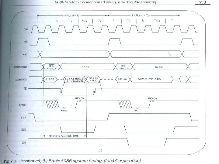
CPU: Instruction Cycle Three basic operations: Fetch: fetches the instruction, copying it from memory into the instruction queue, and increments the PC (program counter) Decode: control unit determines the type of the instruction. Retrieves any needed operands and sends them to the ALU. Also sends the ALU signals to indicate the type of operation. Execute: ALU executes the instruction, returns output to the destination, and update the status flags. Each step takes one click of the System clock: one clock cycle.
Basic Terms in Timing CLK is divided into States. Machine cycle: Time taken for Reading or Writing a byte with Memory or Port. Machine cycle consists of many states. Instruction Cycle: Time taken for fetch, decode, excute an Instruction Cycle consists of many Machine Cycles.
Pin Description AD 0 -AD 15: Multiplexed Address/Data Bus RD’: Low while reading from memory or port WR’ : Low while writing to memory or port. M/IO’ : High during Memory operations. Low during Port operations. ALE : High to enable Address Latches. S 0 -S 2 – Bus Control, INTA, I/O read, I/O write, HALT, code access, memory read, memory write, release bus. S 3 -S 6, QS 0 -QS 1: Status of internal state
Pin Description (Contd) BHE: Combines with A 0 to form the operation for transfer of Address Reset: Causes the processor to immediately terminate its present activity and restarts execution again. Ready: When CPU asks for a byte from memory, memory is expected to deliver within 4 bus cycles. If memory is too slow, it negates Ready and keeps it negated until the byte is put on the bus. DEN’: Output enable for the Data Transceiver. DT/R’: It is used to control the direction of data flow through the transceiver (T = 1, R =0).
Fetching an instruction: CPU puts the address of the instruction on the address pins Asserts “memory read” Memory replies by putting instruction on data pins Asserts a signal that it’s done (READY) When CPU sees the signal, it accepts the word and carries out the instruction
Read Machine Cycle Asserts M/IO’ for reading from Memory or Port. Asserts ALE High to enable Address Latches. Sends desired address on A 0 -A 19 pins. Asserts ALE Low to latch address on external latches. Removes the address from A 0 -A 19 Asserts RD’ Low to output data into data bus. Assets READY Low to send 8086 into wait state.
Read Machine Cycle (Contd. . ) In Wait State, 8086 will wait for addressed memory or port to output data. Asserts Ready High to specify that addressed memory or port has placed data on data bus. DT/R’ is Low to specify that 8086 is receiving the data. DEN’ is Low to enable data buffers for transfer data from addressed memory or port to 8086.
Write Machine Cycle Asserts M/IO’ for writing from Memory or Port. Asserts ALE High to enable Address Latches. Sends desired address on A 0 -A 19 pins. Asserts ALE Low to latch address on external latches. Removes the address from A 0 -A 19 Asserts WR’ Low to output data into data bus. Assets READY Low to send 8086 into wait state.
Write Machine Cycle (Contd. . ) In Wait State, 8086 will wait for addressed memory or port to receive data. Asserts Ready High to specify that addressed memory or port is ready to receive data on data bus. DT/R’ is High to specify that 8086 is transmitting the data. DEN’ is Low to enable data buffers for transfer of data from 8086 to addressed memory or port.
Minimum & Maximum Mode Minimum Mode: MN/MX’ = 1 Processor produces the Control Bus Signals. WR’, M/IO’, DT/R’, DEN’, ALE, INTA’ will be accessed. Maximum Mode: MN/MX’ = 0 External device produces the control bus signals. S 0’, S 1’, S 2’, QS 0’, QS 1’, LOCK’ will be accessed.